

Page 1
In the absence of confirmation by device specification sheets, SHARP takes no responsibility for any defects that may occur in equipment using any SHARP devices shown in
catalogs, data books, etc. Contact SHARP in order to obtain the latest device specification sheets before using any SHARP device.
1
DESCRIPTION
The LZ0P3641/42∫/45∫/46 are 1/4-type (4.5 mm)
350 000-pixel built-in lens color CCD (chargecoupled device) area sensors. All pixel signals can
be read independently via the vertical shift register
and horizontal shift register. With their small lens
and WLCC-type flat package, it is possible to make
ultra small color camera easily.
FEATURES
• Progressive scan
• Square pixel
• Compatible with VGA format
• Number of effective pixels : 659 (H) x 494 (V)
• Number of optical black pixels
– Horizontal : 2 front and 31 rear
– Vertical : 8 front and 2 rear
• Number of dummy bits
– Horizontal : 16
– Vertical : 5
• Pixel pitch : 5.6 µm (H) x 5.6 µm (V)
• R, G and B primary color mosaic filters
• Low fixed-pattern noise and lag
• Blooming suppression structure
• Built-in output amplifier
• Built-in overflow drain voltage circuit and reset
gate voltage circuit
• Horizontal shift register clock and reset gate clock
voltage : 3.3 V (TYP.)
• Variable electronic shutter (1/30 to 1/10 000 s)
• Built-in optical low-pass-filter
• Integrated lens :
Horizontal viewing angle
LZ0P3641/46 : 50˚
∫LZ0P3642 : 62˚
∫LZ0P3645 : 115˚
• Package
– 14-pin half-pitch WLCC
*
type
– Base section size : 12 mm (H) x 11 mm (V)
–
Outline dimensions (MAX.) : 18 mm (H) x 11 mm (V)
• Package height : approx. 13 mm (two pcs. of lenses)
* Window Leadless Chip Carrier
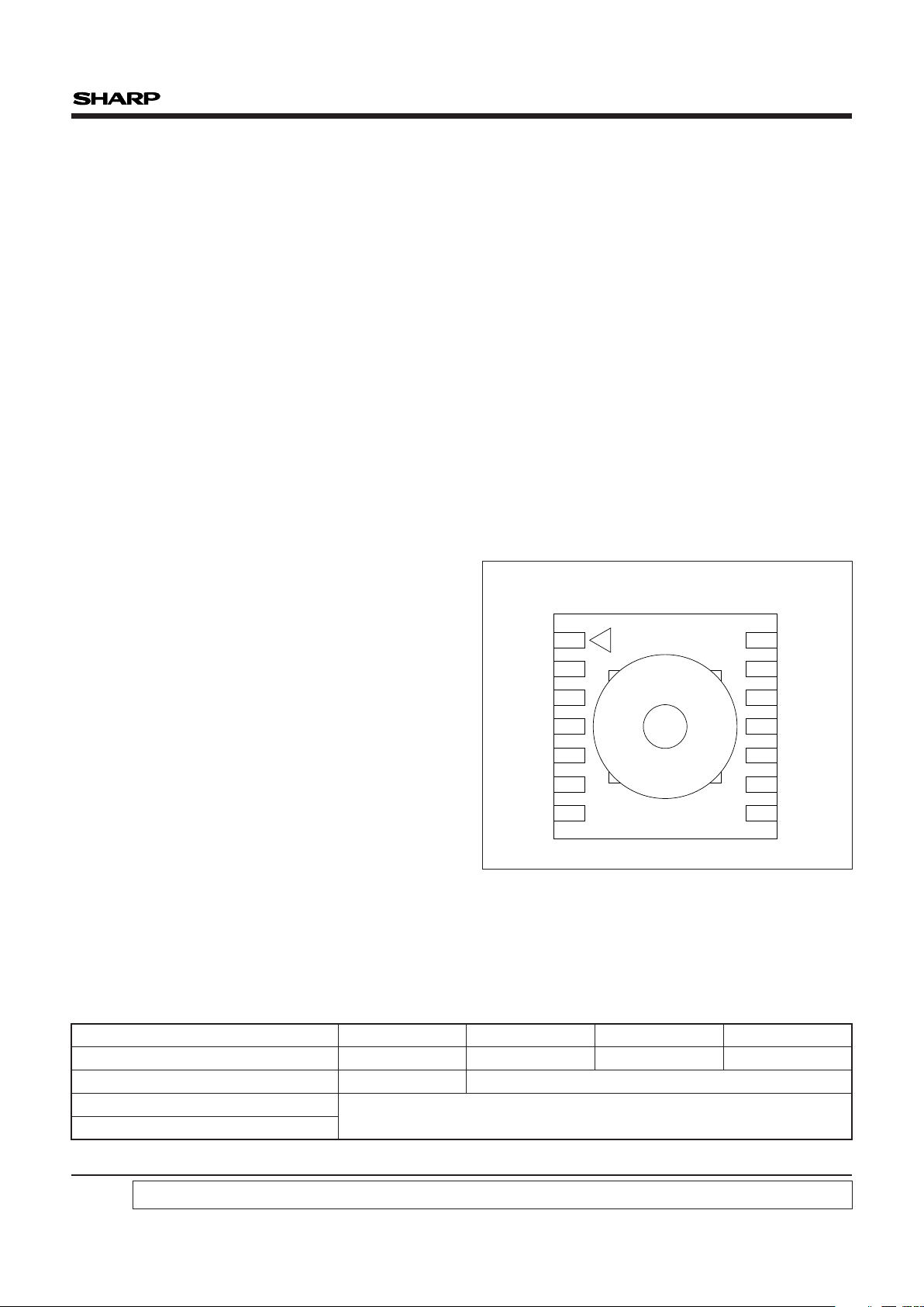
PIN CONNECTIONS
LZ0P3641/3642/3645/3646
LZ0P3641/3642∫/
3645
∫
/3646
1/4-type Built-in Lens Color CCD
Area Sensors with 350 k Pixels
∫Under development
ØV2
Ø
V1
Ø
V3A
Ø
V3B
PW
GND
OS
1
2
3
4
5
6
7
14
13
12
11
10
9
8
Ø
H2
Ø
H1
Ø
RS
NC
OFD
GND
OD
14-PIN HALF-PITCH WLCC TYPE
TOP VIEW
COMPARISON TABLE
Horizontal viewing angle
Lens specification
Characteristics
∫LZ0P3645∫LZ0P3642LZ0P3641
115˚62˚50˚
Refer to each following specification.
50˚
LZ0P3646
3.4 2.8F no.
Page 2
2
LZ0P3641/3642/3645/3646
PIN DESCRIPTION
ABSOLUTE MAXIMUM RATINGS
(TA = +25 ˚C)
SYMBOL PIN NAME
OD Output transistor drain
OS Output signals
ØRS Reset transistor clock
Ø
V1, ØV2, ØV3A, ØV3B Vertical shift register clock
ØH1, ØH2 Horizontal shift register clock
OFD Overflow drain
PW P-well
GND Ground
NC No connection
PARAMETER SYMBOL RATING UNIT
Output transistor drain voltage V
OD 0 to +18 V
Overflow drain voltage V
OFD Internal output V
Reset gate clock voltage VØRS Internal output V
Vertical shift register clock voltage V
ØV –11.5 to +17.5 V
Horizontal shift register clock voltage VØH –0.3 to +12 V
Voltage difference between P-well and vertical clock V
PW-VØV –29 to 0 V
Voltage difference between vertical clocks V
ØV-VØV 0 to +15 V
–20 to +70 ˚CStorage temperature TSTG
–10 to +60 ˚CAmbient operating temperature TOPR
3
2
1
NOTE
NOTES :
1. Do not connect to DC voltage directly. When OFD is connected to GND, connect VOD to GND. Overflow drain clock is
applied below 27 Vp-p.
2. Do not connect to DC voltage directly. When Ø
RS is connected to GND, connect VOD to GND. Reset gate clock is
applied below 8 Vp-p.
3. When clock width is below 10 µs, and clock duty factor is below 0.1%, voltage difference between vertical clocks will be
below 28 V.
Page 3
3
LZ0P3641/3642/3645/3646
RECOMMENDED OPERATING CONDITIONS
PARAMETER SYMBOL MIN. TYP. MAX. UNIT NOTE
Ambient operating temperature T
OPR 25.0 ˚C
Output transistor drain voltage V
OD 14.55 15.0 15.45 V
Overflow drain clock
p-p level V1VØOFD 22.5
Ground GND 0.0 V
P-well voltage V
PW –10.0 VØVL V2
Vertical shift
register clock
LOW level
V
ØV1L, VØV2L
VØV3AL, VØV3BL
–9.5 –9.0 –8.5 V
INTERMEDIATE level
V
ØV1I, VØV2I
VØV3AI, VØV3BI
0.0 V
HIGH level V
ØV3AH, VØV3BH 14.55 15.0 15.45 V
Horizontal shift
register clock
LOW level V
ØH1L, VØH2L –0.05 0.0 0.05 V
HIGH level VØH1H, VØH2H 3.0 3.3 5.5 V
Reset gate clock p-p level V
ØRS V1
Vertical shift register clock frequency
f
ØV1, fØV2
fØV3A, fØV3B
15.73 kHz
Horizontal shift register clock frequency f
ØH1, fØH2 12.27 MHz
Reset gate clock frequency fØRS 12.27 MHz
NOTES :
1. Use the circuit parameter indicated in "SYSTEM CONFIGURATION EXAMPLE", and do not connect to DC voltage directly.
2. V
PW is set below VØVL that is low level of vertical shift register clock, or is used with the same power supply that is connected
to V
L of V driver IC.
* To apply power, first connect GND and then turn on V
OD. After turning on VOD, turn on PW first and then turn on other powers
and pulses. Do not connect the device to or disconnect it from the plug socket while power is being applied.
3.0 3.3 5.5
Page 4
4
LZ0P3641/3642/3645/3646
CHARACTERISTICS FOR LZ0P3641 (1/30 s progressive scan readout mode)
(
TA: +25 ˚C, Operating conditions : The typical values specified in
"RECOMMENDED OPERATING CONDITIONS"
.
Color temperature of light source : 3 200 K)
PARAMETER SYMBOL
Standard output voltage V
O
Saturation output voltage V
SAT
450
MIN. TYP.
150
230150RSensitivity (Green channel) 3
2
1
NOTE
mV
mV
mV
UNITMAX.
8.0 mAOutput transistor drain current I
OD
4.0
%6Shading 45 60
TV line 4Resolution (at center) 250 300
200150Resolution (at corner) 5TV line
Difference of center position 7%±10
NOTES :
1. The average output voltage of G signal in the central
area (H/10, V/10) under uniform illumination.
The standard exposure conditions are defined as when
V
O is 150 mV.
2. The average output voltage of G signal in the central
area (H/10, V/10) under 10 times exposure of the
standard exposure conditions.
3. The average output voltage of G signal in the central
area (H/10, V/10) when a 1 000 lux light source with a
white board of 90% reflector is imaged.
4. The resolution in the central area (H/10, V/10) at which
the image of the TV resolution chart (ex. EIAJ test chart)
can be distinguished on the B/W video monitor when
converted into composite video signals.
5. The resolution in the peripheral area (image height : Y =
0.8) under the conditions mentioned above.
6. Defined by the following formula at the brightness of
standard output voltage : (Vco/Vce) x 100 [%]
Vco : Output voltage at edge of the image (at NTSC
video output).
Vce : Output voltage at center of the image (at NTSC
video output).
7. The difference between the center position of image and
that of the monitor. This is the ratio for the horizontal
underscanning monitor size which includes the decentering
eccentricity when turning the lens head one time.
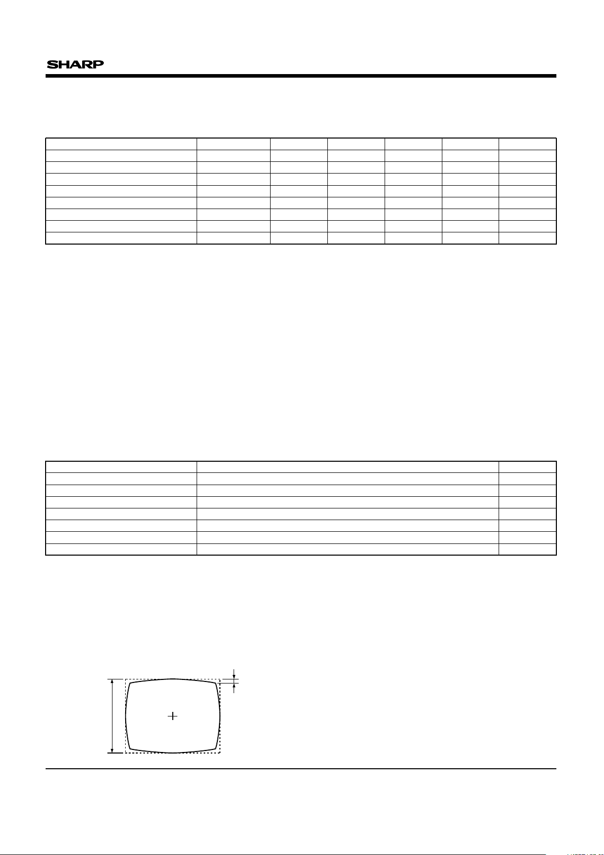
LENS SPECIFICATION FOR LZ0P3641
PARAMETER SPECIFICATION
Construction 2 pcs. (non-spherical, plastic)
Focal length 3.9 mm [TYP. : reference]
NOTE
3.4±5%F No.
Focus adjustment range ∞ to 10 cm 2
TV distortion ≤ –1.0% 1
Viewing angle H : 50˚, V : 38˚, Diagonal : 60˚ [TYP. : reference]
NOTES :
1. TV distortion is defined by the formula, (∆y/y) x 100 [%]
at capturing rectangular pattern sized horizontal by
vertical as 4 by 3.
"y" is defined as the vertical height of the center of the
horizontal line.
∆y is defined as the difference between the vertical height
of the center of the horizontal line and an edge of it.
2. The best focus point of an object can be obtained by
turning the lens head within this range.
3. Torques which are necessary for turning the lens.
* Be careful not to remove the lens head by turning it
counterclockwise too much when adjusting macro.
y
∆y
30.00005 to 0.001 N·mTorque of focusing
Page 5

5
LZ0P3641/3642/3645/3646
CHARACTERISTICS FOR LZ0P3642
∫
(1/30 s progressive scan readout mode)
(
TA: +25 ˚C, Operating conditions : The typical values specified in
"RECOMMENDED OPERATING CONDITIONS"
.
Color temperature of light source : 3 200 K)
NOTES :
1. The average output voltage of G signal in the central
area (H/10, V/10) under uniform illumination.
The standard exposure conditions are defined as when
V
O is 150 mV.
2. The average output voltage of G signal in the central
area (H/10, V/10) under 10 times exposure of the
standard exposure conditions.
3. The average output voltage of G signal in the central
area (H/10, V/10) when a 1 000 lux light source with a
white board of 90% reflector is imaged.
4. The resolution in the central area (H/10, V/10) at which
the image of the TV resolution chart (ex. EIAJ test chart)
can be distinguished on the B/W video monitor when
converted into composite video signals.
5. The resolution in the peripheral area (image height : Y =
0.8) under the conditions mentioned above.
6. Defined by the following formula at the brightness of
standard output voltage : (Vco/Vce) x 100 [%]
Vco : Output voltage at edge of the image (at NTSC
video output).
Vce : Output voltage at center of the image (at NTSC
video output).
7. The difference between the center position of image and
that of the monitor. This is the ratio for the horizontal
underscanning monitor size which includes the decentering
eccentricity when turning the lens head one time.
PARAMETER SYMBOL
Standard output voltage V
O
Saturation output voltage V
SAT
450
MIN. TYP.
150
230150RSensitivity (Green channel) 3
2
1
NOTE
mV
mV
mV
UNITMAX.
8.0 mAOutput transistor drain current I
OD
4.0
%6Shading 40 55
TV line 4Resolution (at center) 250 300
200150Resolution (at corner) 5TV line
Difference of center position 7%±10
LENS SPECIFICATION FOR LZ0P3642
∫
PARAMETER SPECIFICATION
Construction 2 pcs. (non-spherical, plastic)
Focal length 3.0 mm [TYP. : reference]
NOTE
2.8±5%F No.
Focus adjustment range ∞ to 10 cm 2
TV distortion ≤ –1.0% 1
Viewing angle H : 62˚, V : 49˚, Diagonal : 74˚ [TYP. : reference]
NOTES :
1. TV distortion is defined by the formula, (∆y/y) x 100 [%]
at capturing rectangular pattern sized horizontal by
vertical as 4 by 3.
"y" is defined as the vertical height of the center of the
horizontal line.
∆y is defined as the difference between the vertical height
of the center of the horizontal line and an edge of it.
2. The best focus point of an object can be obtained by
turning the lens head within this range.
3. Torques which are necessary for turning the lens.
* Be careful not to remove the lens head by turning it
counterclockwise too much when adjusting macro.
y
∆y
30.00005 to 0.001 N·mTorque of focusing
∫Under development
Page 6

6
LZ0P3641/3642/3645/3646
PARAMETER SYMBOL
Standard output voltage V
O
Saturation output voltage V
SAT
450
MIN. TYP.
150
230150RSensitivity (Green channel) 3
2
1
NOTE
mV
mV
mV
UNITMAX.
8.0 mAOutput transistor drain current I
OD
4.0
%6Shading 40
TV line 4Resolution (at center) 300
200Resolution (at corner) 5TV line
Difference of center position 7%±10
PARAMETER SPECIFICATION
Construction 2 pcs. (non-spherical, plastic)
Focal length 1.53 mm [TYP. : reference]
NOTE
2.8±5%F No.
Focus adjustment range ∞ to 10 cm 2
TV distortion ≤ –14% 1
Viewing angle H : 115˚, V : 89˚, Diagonal : 138˚ [TYP. : reference]
NOTES :
1. TV distortion is defined by the formula, (∆y/y) x 100 [%]
at capturing rectangular pattern sized horizontal by
vertical as 4 by 3.
"y" is defined as the vertical height of the center of the
horizontal line.
∆y is defined as the difference between the vertical height
of the center of the horizontal line and an edge of it.
2. The best focus point of an object can be obtained by
turning the lens head within this range.
3. Torques which are necessary for turning the lens.
* Be careful not to remove the lens head by turning it
counterclockwise too much when adjusting macro.
y
∆y
30.00005 to 0.001 N·mTorque of focusing
CHARACTERISTICS FOR LZ0P3645
∫
(1/30 s progressive scan readout mode)
(
TA: +25 ˚C, Operating conditions : The typical values specified in
"RECOMMENDED OPERATING CONDITIONS"
.
Color temperature of light source : 3 200 K)
NOTES :
1. The average output voltage of G signal in the central
area (H/10, V/10) under uniform illumination.
The standard exposure conditions are defined as when
V
O is 150 mV.
2. The average output voltage of G signal in the central
area (H/10, V/10) under 10 times exposure of the
standard exposure conditions.
3. The average output voltage of G signal in the central
area (H/10, V/10) when a 1 000 lux light source with a
white board of 90% reflector is imaged.
4. The resolution in the central area (H/10, V/10) at which
the image of the TV resolution chart (ex. EIAJ test chart)
can be distinguished on the B/W video monitor when
converted into composite video signals.
5. The resolution in the peripheral area (image height : Y =
0.8) under the conditions mentioned above.
6. Defined by the following formula at the brightness of
standard output voltage : (Vco/Vce) x 100 [%]
Vco : Output voltage at edge of the image (at NTSC
video output).
Vce : Output voltage at center of the image (at NTSC
video output).
7. The difference between the center position of image and
that of the monitor. This is the ratio for the horizontal
underscanning monitor size which includes the decentering
eccentricity when turning the lens head one time.
∫Under development
LENS SPECIFICATION FOR LZ0P3645
∫
Page 7

LZ0P3641/3642/3645/3646
7
CHARACTERISTICS FOR LZ0P3646 (1/30 s progressive scan readout mode)
(
TA: +25 ˚C, Operating conditions : The typical values specified in
"RECOMMENDED OPERATING CONDITIONS"
.
Color temperature of light source : 3 200 K)
PARAMETER SYMBOL
Standard output voltage V
O
Saturation output voltage V
SAT
450
MIN. TYP.
150
230150RSensitivity (Green channel) 3
2
1
NOTE
mV
mV
mV
UNITMAX.
8.0 mAOutput transistor drain current I
OD
4.0
%6Shading 45 60
TV line 4Resolution (at center) 250 300
200150Resolution (at corner) 5TV line
Difference of center position 7%±10
NOTES :
1. The average output voltage of G signal in the central
area (H/10, V/10) under uniform illumination.
The standard exposure conditions are defined as when
V
O is 150 mV.
2. The average output voltage of G signal in the central
area (H/10, V/10) under 10 times exposure of the
standard exposure conditions.
3. The average output voltage of G signal in the central
area (H/10, V/10) when a 1 000 lux light source with a
white board of 90% reflector is imaged.
4. The resolution in the central area (H/10, V/10) at which
the image of the TV resolution chart (ex. EIAJ test chart)
can be distinguished on the B/W video monitor when
converted into composite video signals.
5. The resolution in the peripheral area (image height : Y =
0.8) under the conditions mentioned above.
6. Defined by the following formula at the brightness of
standard output voltage : (Vco/Vce) x 100 [%]
Vco : Output voltage at edge of the image (at NTSC
video output).
Vce : Output voltage at center of the image (at NTSC
video output).
7. The difference between the center position of image and
that of the monitor. This is the ratio for the horizontal
underscanning monitor size which includes the decentering
eccentricity when turning the lens head one time.
LENS SPECIFICATION FOR LZ0P3646
PARAMETER SPECIFICATION
Construction 2 pcs. (non-spherical, plastic)
Focal length 3.9 mm [TYP. : reference]
NOTE
2.8±5%F No.
Focus adjustment range ∞ to 10 cm 2
TV distortion ≤ –1.0% 1
Viewing angle H : 50˚, V : 38˚, Diagonal : 60˚ [TYP. : reference]
NOTES :
1. TV distortion is defined by the formula, (∆y/y) x 100 [%]
at capturing rectangular pattern sized horizontal by
vertical as 4 by 3.
"y" is defined as the vertical height of the center of the
horizontal line.
∆y is defined as the difference between the vertical height
of the center of the horizontal line and an edge of it.
2. The best focus point of an object can be obtained by
turning the lens head within this range.
3. Torques which are necessary for turning the lens.
* Be careful not to remove the lens head by turning it
counterclockwise too much when adjusting macro.
y
∆y
30.00005 to 0.001 N·mTorque of focusing
Page 8

PIXEL STRUCTURE
,,,,,,,
,
,,,,,,,
,
,,,,,,,
,
,,,,,,,
,
yyyyyyy
y
yyyyyyy
y
yyyyyyy
y
yyyyyyy
y
659 (H) x 494 (V)
OPTICAL BLACK
(2 PIXELS)
OPTICAL BLACK
(8 PIXELS)
1 pin
OPTICAL BLACK
(2 PIXELS)
OPTICAL BLACK
(31 PIXELS)
COLOR FILTER ARRAY
GBGBG
RGRGR
GBGBG
RGRGR
GBGBG
RGRGR
GBGBG
RGRGR
GBGBG
RGRGR
GBGBG
RGRGR
GBGBG
RGRGR
GBGBG
RGRGR
GBGBG
RGRGR
GBGBG
RGRGR
GBGBG
RGRGR
GBGBG
RGRGR
(1, 494) (659, 494)
(1, 1) (659, 1)
LZ0P3641/3642/3645/3646
8
Page 9

LZ0P3641/3642/3645/3646
9
TIMING CHART
OS
Ø
OFD
ØV3A
ØV3B
ØV2
ØV1
VD
HD
VERTICAL TRANSFER TIMING
5251102030
492
493
494
OB1
OB2 D1D2D3D4D5
OB1
OB2
OB3
OB4
OB5
OB6
OB7
OB8
12
OS
ØRS
ØH2
ØH1
HD
OB (31)
ØOFD
ØV3A
ØV3B
ØV2
ØV1
HORIZONTAL TRANSFER TIMING
35
780, 1 78
35 107
47
59 95
72 95
83
OUTPUT (659) 1
ππππππππππ
OB (2)
PRE SCAN (16)
71
πππππ
659
ØV3A
ØV3B
ØV2
ØV1
HD
READOUT TIMING
39.8 µs (489 bits)
46.9 µs (576 bits)
63.5 µs (780 bits)
(62 bits)
5.05 µs
Page 10

LZ0P3641/3642/3645/3646
10
SYSTEM CONFIGURATION EXAMPLE
OD
OFD
Ø
V2
ØV1
GND
NC
Ø
H1
ØH2
OS
GND
PW
Ø
V3B
ØV3A
ØRS
V3B
V3A
V1B
V1A
VMa
VH
V4
V2
VL
VMb
POFD
NC
VH
ØH2
V1X
V3X
V2X
VH3BX
VH3AX
+5 V
OFDX
ØH1
ØRS
VL (VPW)
CCD
OUT
VOFDH
VH3BX
OFDX
V
2X
V1X
V3X
VDD
GND
V
4X
VH3AX
VH1BX
VH1AX
+
+
1234567812
242322212019181713
11
14
10
15
9
16
91011121314
65
8
74321
LR36685
LZ0P364X
(*1)(*1)
VOD
270 pF
100 $
1 M$
1 M$
0. 47 µF
0.01 µF
+
+
(*2)
(*2) (*3)
(*3)
(*1) ØRS, OFD :
Use the circuit parameter indicated in this circuit example, and do
not connect to DC voltage directly.
(*2) Connect V
1X of timing generator to V4X of V driver IC,
LR36685.
(*3) Connect V
4 of V driver IC to ØV1 of LZ0P364X.
Page 11

PACKAGES FOR CCD AND CMOS DEVICES
11
,,,,,,,,,,,,,,,,,,,,,,,,,,,
,
,,,,,,,,,,,,,,,,,,,,,,,,,,,
,
,,,,,,,,,,,,,,,,,,,,,,,,,,,
,
,,,,,,,,,,,,,,,,,,,,,,,,,,,
,
,,,,,,,,,,,,,,,,,,,,,,,,,,,
,
,,,,,,,,,,,,,,,,,,,,,,,,,,,
,
,,,,,,,,,,,,,,,,,,,,,,,,,,,
,
,,,,,,,,,,,,,,,,,,,,,,,,,,,
,
,,,,,,,,,,,,,,,,,,,,,,,,,,,
,
,,,,,,,,,,,,,,,,,,,,,,,,,,,
,
,,,,,,,,,,,,,,,,,,,,,,,,,,,
,
,,,,,,,,,,,,,,,,,,,,,,,,,,,
,
,,,,,,,,,,,,,,,,,,,,,,,,,,,
,
,,,,,,,,,,,,,,,,,,,,,,,,,,,
,
,,,,,,,,,,,,,,,,,,,,,,,,,,,
,
,,,,,,,,,,,,,,,,,,,,,,,,,,,
,
,,,,,,,,,,,,,,,,,,,,,,,,,,,
,
,,,,,,,,,,,,,,,,,,,,,,,,,,,
,
,,,,,,,,,,,,,,,,,,,,,,,,,,,
,
,,,,,,,,,,,,,,,,,,,,,,,,,,,
,
,,,,,,,,,,,,,,,,,,,,,,,,,,,
,
,,,,,,,,,,,,,,,,,,,,,,,,,,,
,
,,,,,,,,,,,,,,,,,,,,,,,,,,,
,
,,,,,,,,,,,,,,,,,,,,,,,,,,,
,
,,,,,,,,,,,,,,,,,,,,,,,,,,,
,
,,,,,,,,,,,,,,,,,,,,,,,,,,,
,
,,,,,,,,,,,,,,,,,,,,,,,,,,,
,
,
,
,
,
,
,
,
,
,
,
,
,
,
,
,
,
,
,
,
,
,
,
,
,
,,,,,,
,
,,,,,,
,
,
,,
,
,,
,
,,
,,,
,,,
,,,
,,,
,
,
,
,
,
,
,
,
,
,
,
,
,
,
,
,
,
,
,
,
,
,
,
,
,
,
,
,
,
,
,
,
,
,
,
,
,
,
,
,
,
,
,
,
,
,
,
,
,,,
,,,
,,,
,,,
,
,
,
,
,
,
,
,
,
,
,
,
,
,
,
,
,
,
,
,
,
,
,
,
,
,
,
,
,
,
,,,
,,,
,,,
,,,
,
,
,
,
,
,
,
,
,
,
,
,
,
,
,
,
,
,
18
11
3.0
±0.1
5.0
±0.1
Approx.12-13
2-Ø0.8
0.8
1.6
2-C0.2
14
±0.1
12
4-90˚
5.0
±0.1
Approx. 12
11.0
±0.05
Height 0.5
3.0
±0.1
1.0
±0.1
2.0
±0.1
11
±0.05
7.6
±0.05
3.6
1.27
0.64
1.27
2.0
±0.1
+0
–0.2
+0
–0.1
+0
–0.05
+0
–0.05
+0
–0.05
+0
–0.1
+0
–0.05
No.1 index
Ø11.0
Ø12.0
+0
–0.05
+0
–0.05
No.1 index
14 WLCC TYPE
¿Applicable models¡
LZ0P3611/12/15,
LZ0P3621/22/25,
LZ0P3641/42/45/46
PACKAGE (Unit : mm)
Page 12

PRECAUTIONS FOR BUILT-IN LENS CCD AREA SENSORS
12
PRECAUTIONS FOR BUILT-IN LENS CCD
AREA SENSORS
1. Package Breakage
In order to prevent the package, the lens holder,
and the lens from being broken, follow the
instructions below :
1) The CCD is a precise optical component and
the package-base material is ceramic.
Therefore,
øTake care not to drop the device when
mounting, handling, or transporting.
øAvoid giving a shock to the package.
Especially when leads are fixed to the socket
or the circuit board, a small shock could
break the package more easily than when the
package isn’t fixed.
2) When adjusting the focus, screw the lens holder
to the circuit board before soldering the leads.
At that time, make sure to use a circuit board
with plenty of strength, and to avoid the
package and the lens holder from being broken,
the following screw and clamp torque are
recommended.
ø Recommended mounting screw :
Ø1.7 tapping screw (B-tight type),
Length, L = the thickness of the circuit board
+ 5 mm
ø Recommended clamp torque : 0.012 N·m
[however, when the thickness of the circuit
board is thinner than t = 2.0 mm]
3) If any damage or breakage occurs on the
surface of the lens, its characteristics could
deteriorate.
Therefore,
ø Do not hit the lens.
ø Do not give a shock large enough to cause
distortion.
ø Do not scrub or scratch the surface of the
lens.
– Even a soft cloth or applicator, if dry, could
cause dust to scratch the lens.
2. Electrostatic Damage
As compared with general MOS-LSI, CCD has
lower ESD. Therefore, take the following anti-static
measures when handling the CCD :
1) Always discharge static electricity by grounding
the human body and the instrument to be used.
To ground the human body, provide resistance
of about 1 M$ between the human body and
the ground to be on the safe side.
2) When directly handling the device with the
fingers, hold the lens holder and do not touch
the lead.
3) To avoid generating static electricity,
a. do not scrub the device with cloth or plastic.
b. do not attach any tape or labels.
c. do not clean the device with dust-cleaning
tape.
4) When storing or transporting the device, put it in
a container of conductive material.
3. Dust and Contamination
Dust or contamination on the surface of the lens
and the inside of the lens holder could deteriorate
the output characteristics or cause a scar. In order
to minimize dust or contamination on the device,
take the following precautions :
1) Do not remove the lens from the body.
Especially when adjusting macro, be careful not
to remove the lens by turning it counterclockwise too much.
2) Do not touch the surface of the lens with the
fingers. If dust or contamination gets on the
surface of the lens, the following cleaning
method is recommended :
ø Handle the built-in lens CCD in a clean
environment such as a cleaned booth. (The
cleanliness level should be, if possible, class
1 000 at least.)
Page 13

– In case where the soldering may exceed the
time mentioned above, resume the work
after the device returns to normal
temperature.
ø Do not put too much force onto the lens and
the lens holder while soldering.
ø Be careful not to let the soldering iron touch
the lens holder.
– Soldering can be quickly/neatly done by
laying the soldering iron so it lightly touches
the border between the package and the
circuit board and sliding it in sideways.
2) There is no guarantee of the performance of
the device which has been removed or
resoldered after being soldered once under the
conditions mentioned above.
– In case there seems to be an inferior device,
consult with our sales office before removing
it.
3) Avoid using or storing the CCD at high
temperature or high humidity as it is a precise
optical component. Do not give a mechanical
shock to the CCD.
4) Do not expose the device to strong light. For
the color device, long exposure to strong light
will fade the color of the color filters.
ø Dust from static electricity should be blown
off with an ionized air blower. For antielectrostatic measures, however, ground all
the leads on the device before blowing off
the dust.
ø The contamination on the surface of the lens
should be wiped off with a clean applicator
soaked in isopropyl alcohol. Wipe slowly and
gently in one direction only.
– Frequently replace the applicator and do not
use the same applicator to clean more than
one device.
ø Make sure there is no dust or contamination
on the lens and screw it on the lens holder.
4. Other
1) Soldering should be manually performed under
the following conditions :
ø Use ESD-measured soldering iron
ø The conditions of the soldering time in which
the soldering iron touches the package,
differs by the shape and the temperature of
the iron end. Refer to the table below and
take great care in soldering.
THE SHAPE OF
THE IRON END
Below 275 ˚C
Below 300 ˚C
Below 350 ˚C
THE TEMPERATURE OF
THE IRON END
SOLDERING TIME
Time touching the package should be less than 40 seconds
Time touching the package should be less than 25 seconds
Time touching the package should be less than 35 seconds
17
R0.5
(Unit : mm)
17
(Unit : mm)
6.5
0.5
Ø3.2
PRECAUTIONS FOR BUILT-IN LENS CCD AREA SENSORS
13
 Loading...