

LA1060
Ordering number : EN2650B
Antenna Switching Diversity Circuit
for Car-Use FM Tuners
Monolithic Linear IC
SANYO Electric Co.,Ltd. Semiconductor Bussiness Headquarters
TOKYO OFFICE Tokyo Bldg., 1-10, 1 Chome, Ueno, Taito-ku, TOKYO, 110 JAPAN
82997HA (KT)/7119YT/D147TA/N196AT, TS No.2650-1/8
Functions
• Noise amp, noise AGC circuit, noise density circuit.
• Antenna switching trigger output circuit.
• Antenna switching T flip-flop circuit.
• Antenna holding function to be used at weak input signal
reception mode, forced antenna holding function.
Features
• "Count system"-used, reliable detection of multipath
distortion.
• One-tuner type diversity system allowing cost reduction
of sets.
• The output to hold the antenna at the weak input signal
mode and the output (antenna switching trigger output) to
indicate that the antenna switching frequency is high are
delivered at the same pin, allowing a wide variety of
applications according to the design concept of set.
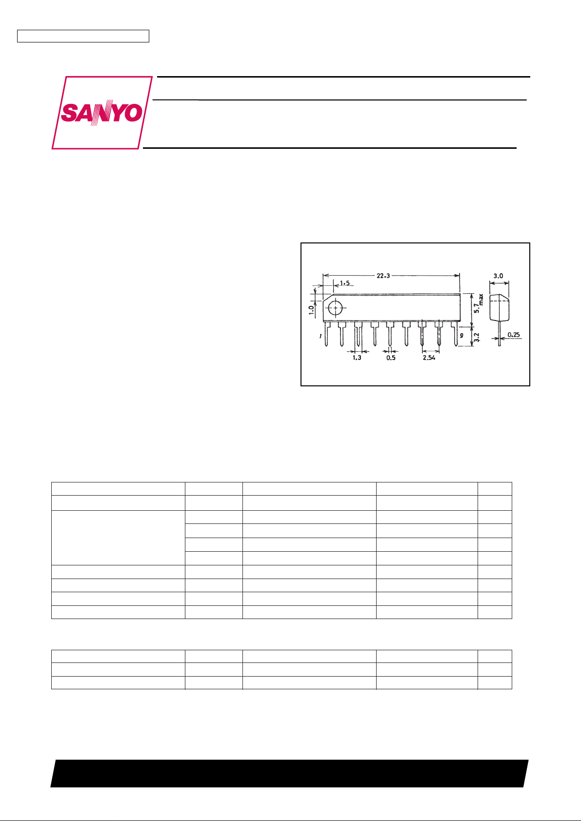
Package Dimensions
unit: mm
3017B-SIP9
[LA1060]
SANYO: SIP9
Specifications
Maximum Ratings
at Ta=25°C
Parameter Symbol Conditions Ratings Unit
Maximum supply voltage VCCmax 16 V
Maximum flow-out I4max 1 mA
I6max 2 mA
I7max 10 mA
I8max 10 mA
Maximum flow-in current I6max 10 mA
Allowable power dissipation Pd max Ta≤75°C 200 mW
Operating temperature Topr –20 to +75 °C
Storage temperature Tstg –40 to +125 °C
Operating Conditions at Ta=25°C
Parameter Symbol Conditions Ratings Unit
Recommended supply voltage V
CC
8V
Operating voltage range VCCop 6.5 to 15 V
LA1060
Electrical Characteristics at Ta=25°C, V
CC
=8.0V, f=100kHz sine wave
Parameter Symbol Conditions
Ratings
min typ max
Unit
Current drain I
CC
No input, not including pins 3.8 4.9 6.0 mA
7, 8 current
Pin 7 high voltage V7
H
Pin 7-GND resistance=1kΩ 5.0 6.0 7.0 V
Pin 8 high voltage V8
H
Pin 8-GND resistance=1kΩ 5.0 6.0 7.0 V
Noise amp gain VG1 Input=3mVrms *1 33 36 39 dB
VG2 Input=100mVrms *1 10 13 16 dB
Noise detection sensitivity NDS Noise AGC=OFF 9 12 15 mVrms
Input signal level at which the
output at pins 7, 8 starts to be
inverted *2
Number of noise counts NCN Input=30mVrms 10
Number of sine waves which
causes the output at pins 7, 8 to be
inverted *2
Gate time t
G
Noise AGC=OFF 100 120 140 µs
Repetitive period of pin 4 waveform
Pin 6 voltage V6 Input=100mVrms *3 1.6 2.0 2.5 V
Antenna holding HLD Input=100mVrms, noise AGC=OFF 5.0 6.0 7.0 V
Pin 8 output voltage *4
Note
*1 : S1=OFF S2=OFF S3=ON S4=OFF S5=OFF
*2 : S1=OFF S2=ON S3=OFF S4=ON S5=OFF
*3 : S1=OFF S2=OFF S3=OFF S4=ON S5=OFF
*4 : S1=OFF S2=ON S3=OFF S4=ON S5=ON
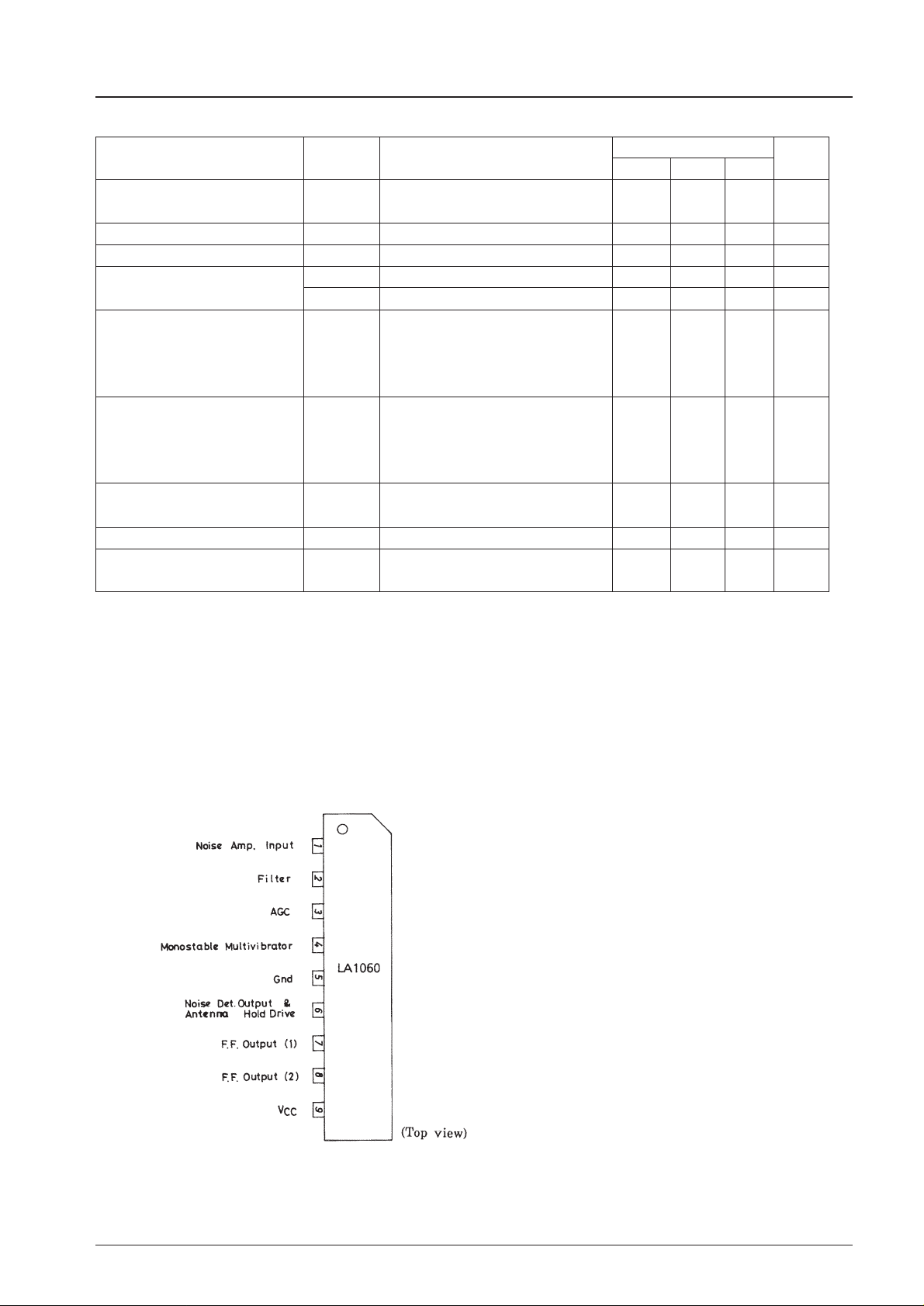
Pin Assignment
No.2650-2/8
LA1060
No.2650-3/8
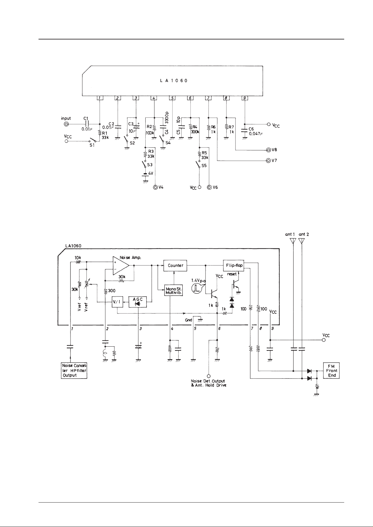
AC Characteristics Test Circuit Diagram
Block Diagram
Unit (resistance : Ω, capacitance : F)
Unit (resistance : Ω, capacitance : F)

LA1060
No.2650-4/8
Sample Application Circuit 1
Component Placement Diagram
R1, Q1, R5, R10, R11 are connected to the Cu-foiled side.
(Because no holes are made.)
Unit (resistance : Ω, capacitance : F)
When the SW is placed in the 300kΩ position, the antenna is
held on the pin 8 side at the weak input signal mode.
When the SW is placed in the 10kΩ position, the antenna
holding function at the weak input signal mode does not work.
Circuit to cause the separation control
at the MPX stage to be entered into the
forced monaural mode when the
antenna switching frequency is high.
The antenna switching trigger pulse at
pin 6 is peak-held, integrated, and
attacks the separation control pin.

LA1060
No2650-5/8
Noise Detection Method of the LA1060
(1) "Count system"-used noise detection
• The LA 1060 is so designed as to count the noise components of 100kHz or greater in the IF output to detect the
multipath distortion.
• Car-use FM tuners are always affected by noises shown below.
(1) Ignition noise
(2) Noise attendant on modulation.
The actual modulation signal is not a continuous wave, but an intermittent signal. When the modulation signal
rises in a burst fashion, the high frequency noise components are detected in the FM demodulation output
(because in a burst fashion, overmodulation may occur or the signal rise characteristic may include the high
frequency components.)
(3) Random noise
The random noise at the weak input signal mode includes some noise components whose peak value is two to
three times as high as the average noise level.
• As a result of checking the above-mentioned noises, we found that the noise of more than a given level being
present within a given period of time (example : within 100µ s) is included in the FM demodulation output of caruse FM tuners at less than a given density only.
• By contrast, when the multipath distortion or skip noise occurs, the continuous noise components occur and the
above-mentioned noise density increases.
• Therefore, by using "count system" to count the noise density, the detection of multipath distortion and skip noise
detection can be performed with less malfunction.
(2) Noise detection time
• It is desirable that the noise detection time is faster (Note 1). However, the noise detection time (noise count time)
of the LA1060 is approximately 100µ s so that the above-mentioned three types of noise cause no malfunction to
occur.
(Note 1) • If the period of noise duration is 20µ s or less, the noise is hardly offensive to the ears. If the period of noise
duration is 50 to 200µs, the noise is heard as a sound "buzz", but a single noise is hardly offensive to the ears.
• If the period of noise duration is 500µ s or more, the noise is heard as a sound "zah" which is offensive to the
ears.
Sample Application Circuit 2
Unit (resistance : Ω, capacitance : F)

LA1060
No.2650-6/8
Sample Application Circuit 3
Unit (resistance : Ω, capacitance : F)
Pin 1 input voltage, V1IN– dBµ
Frequency, f – Hz
Resistance, R8 – Ω
Voltage gain, VG – dB
Voltage gain, VG – dB
Pin 8 voltage, V8(High) – V
Pin 1 input voltage, V1IN– dBµ
Pin 3 voltage, V3 – V
Pin 6 voltage, V6 – V

LA1060
No.2650-7/8
Pin 4 capacitance, C4 – nF
Gate time, t
G
– µs
Ambient temperature, Ta – °C
Voltage gain, VG – dB
Supply voltage, VCC– V
Voltage gain, VG – dB
Tuner input – dBµ
IF OUT noise output (LA1140) – mV
Tuner input – dBµ
H.P.F OUT noise output (LA2110 Pin 10) – mV
Supply voltage, VCC– V
Pin 6 voltage, V6 – V
Ambient temperature, Ta – °C
Pin 6 voltage, V6 – V
Resistance, R – kΩ
Gate time, t
G
– µs

LA1060
No.2650-8/8
Note for Application
1. Noise sensitivity setting
When the LA1060 is used in conjunction with the LA2110, it is unnecessary to adjust the sensitivity. However, if any
malfunction occurs, increase the noise sensitivity control VR form 0Ω to 50kΩ—100kΩ to decrease the input noise
level.
2. Gate time setting
The recommended gate time is 120µs. If any malfunction occurs, shorten the gate time, and less malfunction will
result. If the gate time is made longer, the multipath distortion detection sensitivity is increased. The gate time can be
set by varying the value of the capacitor or resistor connected to pin 4.
3. Antenna holding function
a. To hold the antenna at the weak input signal mode, set the value of the resistor connected to pin 6 to approximately
300kΩ. In this case, the pin 8 output is brought to High level. The antenna input level at which the antenna is held
can be adjusted by varying the value (300kΩ) of the resistor.
b. To switch the antenna even at the weak input signal mode, set the value of the resistor connected to pin 6 to
approximately 10kΩ.
4. Forced antenna holding
Set the pin 6 voltage to 2.5V or greater (example : connect to VCCthrough 10kΩ), and the antenna can be held on the
pin 8 side,
No products described or contained herein are intended for use in surgical implants, life-support systems,
aerospace equipment, nuclear power control systems, vehicles, disaster/crime-prevention equipment and
the like, the failure of which may directly or indirectly cause injury, death or property lose.
Anyone purchasing any products described or contained herein for an above-mentioned use shall:
Accept full responsibility and indemnify and defend SANYO ELECTRIC CO., LTD., its affiliates,
subsidiaries and distributors and all their officers and employees, jointly and severally, against any
and all claims and litigation and all damages, cost and expenses associated with such use:
Not impose any responsibilty for any fault or negligence which may be cited in any such claim or
litigation on SANYO ELECTRIC CO., LTD., its affiliates, subsidiaries and distributors or any of
their officers and employees jointly or severally.
Information (including circuit diagrams and circuit parameters) herein is for example only; it is not guaranteed for volume production. SANYO believes information herein is accurate and reliable, but no guarantees
are made or implied regarding its use or any infringements of intellectual property rights or other rights of
third parties.
This catalog provides information as of August, 1997. Specifications and information herein are subject to
change without notice.
Tuner input – dBµ
Pin 3 (AGC) voltage, V3(AGC) – V
 Loading...