

Page 1
LA1235
Ordering number : EN873F
FM IF System Applications
Monolithic Linear IC
SANYO Electric Co.,Ltd. Semiconductor Bussiness Headquarters
TOKYO OFFICE Tokyo Bldg., 1-10, 1 Chome, Ueno, Taito-ku, TOKYO, 110 JAPAN
O2097HA (KT)/63095HA (KOTO) /O076AT/8044KI, TS/4241KI/3091KI No.873-1/12
Overview
The LA1235 is a high integrated IC developed for use in
high S/N, low distortion FM IF system applications. This
IC features S/N=88dB, distortion factor=0.015% and has
almost all functions required for FM tuner IF stage.
The IF amplifier and limiter stage consist of 6 stages of
double ended differential amplifier having an excellent
AMR, and this stage is followd by the signal meter driver
which consists of 4 stages of level detector, thereby
creating extended linearity up to strong input. The FM
detector stage consists of a double balanced quadrature
detector to which a low frequency preamplifire and a
muting controller are attached. The muting drive stage
consists of an OR circuit for weak signal muting drive
output which detects signal intensity and detuning muting
drive output which detects S curve DC output and enables
the prevention of noise at the time of weak signal and
detuning. Further, the weak signal muting drive output
circuit contains a Schmitt circuit having hysteresis and
enables the prevention of muting malfunction due to
amplitude component at the time of weak signal. The AFC
output and tuning meter drive stage is of current drive type
which makes it possible to adjust AFC sensitivity and
muting band width by means of an external resistor, and
the built-in tuning meter null (short) circuit foreces the
tuning meter to be [0] when th IF amplifier stops working.
The IF amplifier stop circuit, being a circuit to stop the FM
IF amlifier at the time of AM reception, makes it possible
to decrease shock noise due to FM-AM receiving mode
switchover.
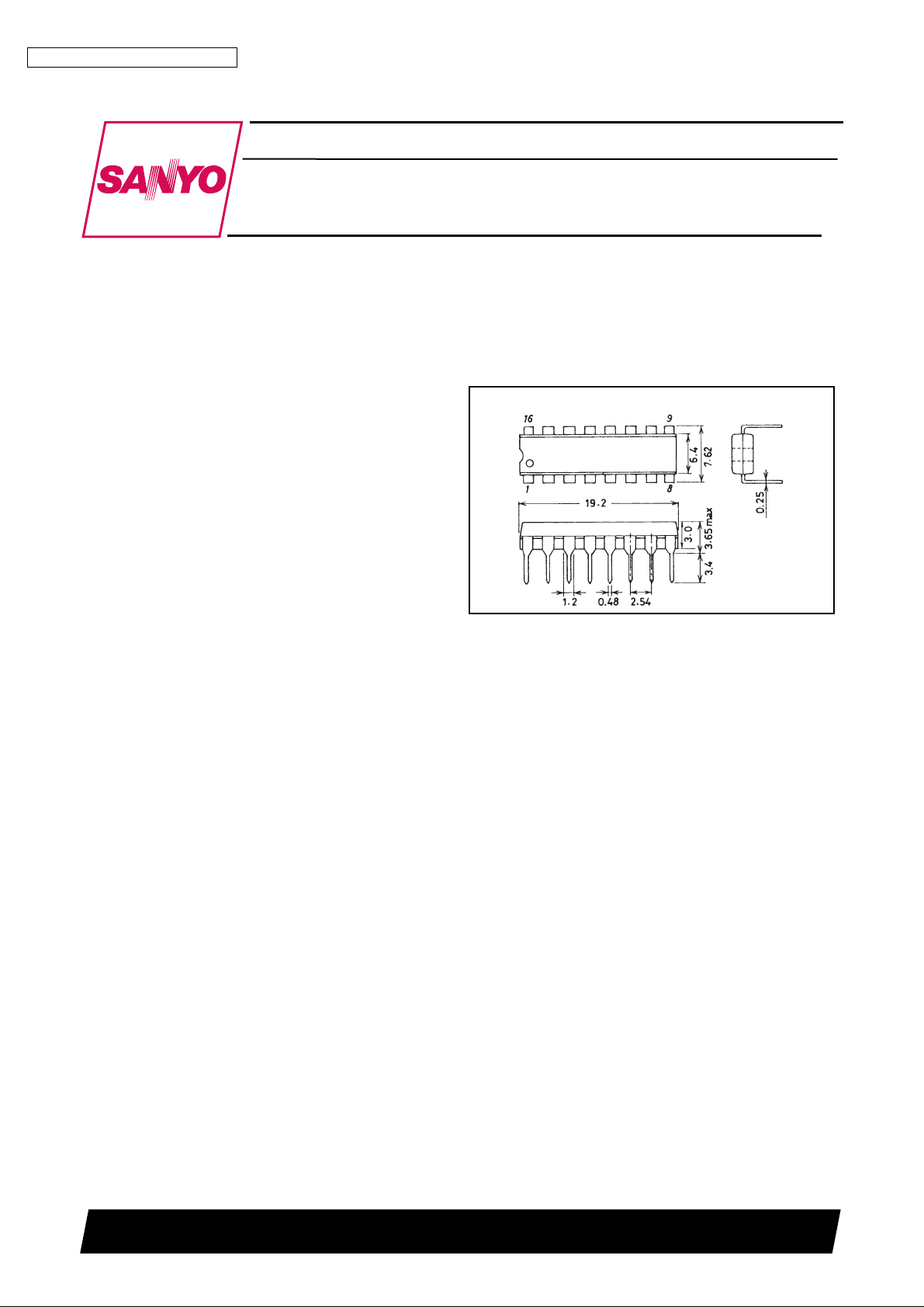
Package Dimensions
unit: mm
3006B-DIP16
[LA1235]
SANYO: DIP16
Functions
• IF amplifier, Limiter.
• Quadrature detection.
• AF preamplifier.
• Signal intesity muting drive output.
• Detuning muting drive output.
• AF signal muting circuit.
• Signal meter drive output.
• AFC, tuning meter drive output.
• IF amplifier stop circuit.
• Tunig meter null circuit.
Features
• High S/N (88dB typ.).
• Low distortion (0.015% typ.).
• Weak signal muting dirve output having hysteresis.
• Tuning mete null (short) circuit.
• Signal meter dirve output having wide dynamic range.
• High limiting sensitivity.
• Built-in constant-voltage regulated circuit (Operating
voltage : 10 to 14V).
Page 2

Specifications
Maximum Ratings
at Ta=25°C
Parameter Symbol Conditions Ratings Unit
Maximum supply voltage V
CC
max Pin 11 16 V
Input voltage V
IN
Pins 1 to 2 ±1 Vp-p
Supply current I
CC
Pin 11 40 mA
Flow-in current I
5
Pin 5 3 mA
Flow-out current I
10
Pin 10 2 mA
I
13
2 mA
Allowable power dissipation Pd max 650 mA
Operating temperature Topr –20 to +70 °C
Storage temperature Tstg –40 to +125 °C
Recommended Operating Conditions at Ta=25°C
Parameter Symbol Conditions Ratings Unit
Recommended supply voltage V
CC
10 to 14 V
Operating Characteristics at Ta=25°C, V
CC
=12V, f=10.7MHz
Parameter Symbol Conditions
Ratings
min typ max
Unit
Quiescent current I
CCO
Quiescent 21 30 mA
Current drain I
CC
VIN=100dBµ 22 31 mA
Detection output V
O
VIN=100dBµ, 400Hz, 100% mod. 310 430 590 mVrms
S/N V
IN
=100dBµ, 400Hz, 100% mod. 82 88 dB
–3dB limiting sensitivity V
IN(lim)
VO: –3dB, 400Hz, 100% mod. 25 31 dBµ
Muting sensitivity V
IN(mute)V12
=5.6V, R16=56kΩ, R15=50kΩ 40 50 dBµ
Muting attenuation mute(att) V
IN
=100dBµ, 400Hz, 100% mod. 80 100 dB
V
5
=3.5V
Muting bandwidth BW(mute) V
IN
=100dBµ, V12=3V 120 200 330 kHz
Muting driving output V
12(1)
Quiescent 5.6 6.2 6.8 V
V
12(2)
VIN=100dBµ 0 0.3 V
Total harmonic distortion THD V
IN
=100dBµ, 400Hz, 100% mod. 0.015 0.05 %
AM supperssion ratio AMR V
IN
=80dBµ, FM =400Hz, 100% mod, 45 60 dB
AM =1kHz, 30% mod.
Signal meter driving output V
13(1)
Quiescent 0 0.1 V
V
13(2)
VIN=35dBµ 0.1 0.5 V
V
13(3)
VIN=70dBµ 1.3 2.0 2.9 V
V
13(4)
VIN=100dBµ 2.2 3.5 5.0 V
Offset voltage V
6-10
Quiescent, pin 6 to 10 –0.8 0 +0.8 V
V
7-10
Quiescent, pin 7 to 10 –0.4 0 +0.4 V
Tuning meter null voltage V
7-10(null)
V5=7.5V, pin 7 to 10 –50 +5 +50 mV
IF-off voltage I
15(IF off)V2-3
=1V 5.6 7.5 V
LA1235
No.873-2/12
Page 3
LA1235
No.873-3/12
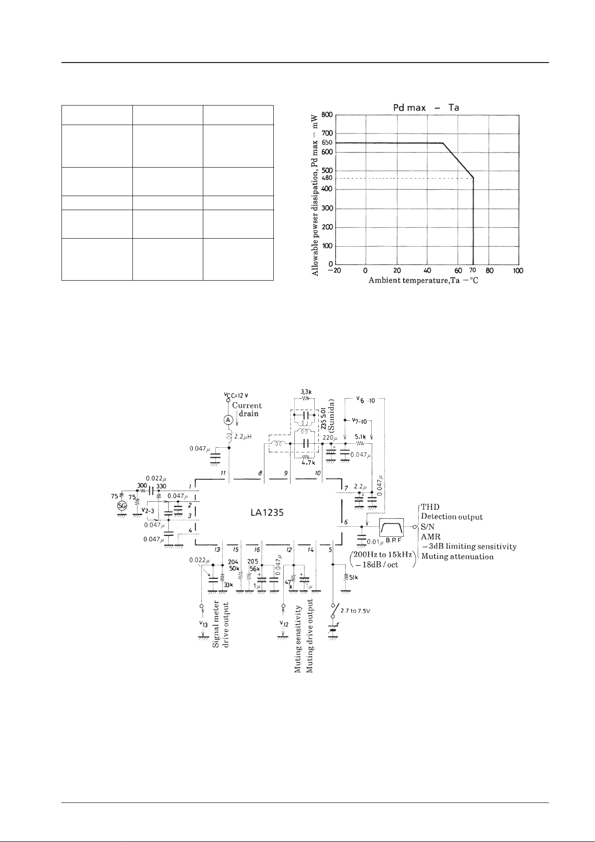
Reference Pin Voltage
Unit (resistance : Ω, capacitance : F)
Pin No.
V
1
V
2
V
3
Quiescent
V
6
V
7
V
8
V
10
V
12
V
13
V
15
V
16
2.6
6.2
5.9
6.2
0
Condition Pin voltage (V)
Test Circuit
Page 4
LA1235
No.873-4/12
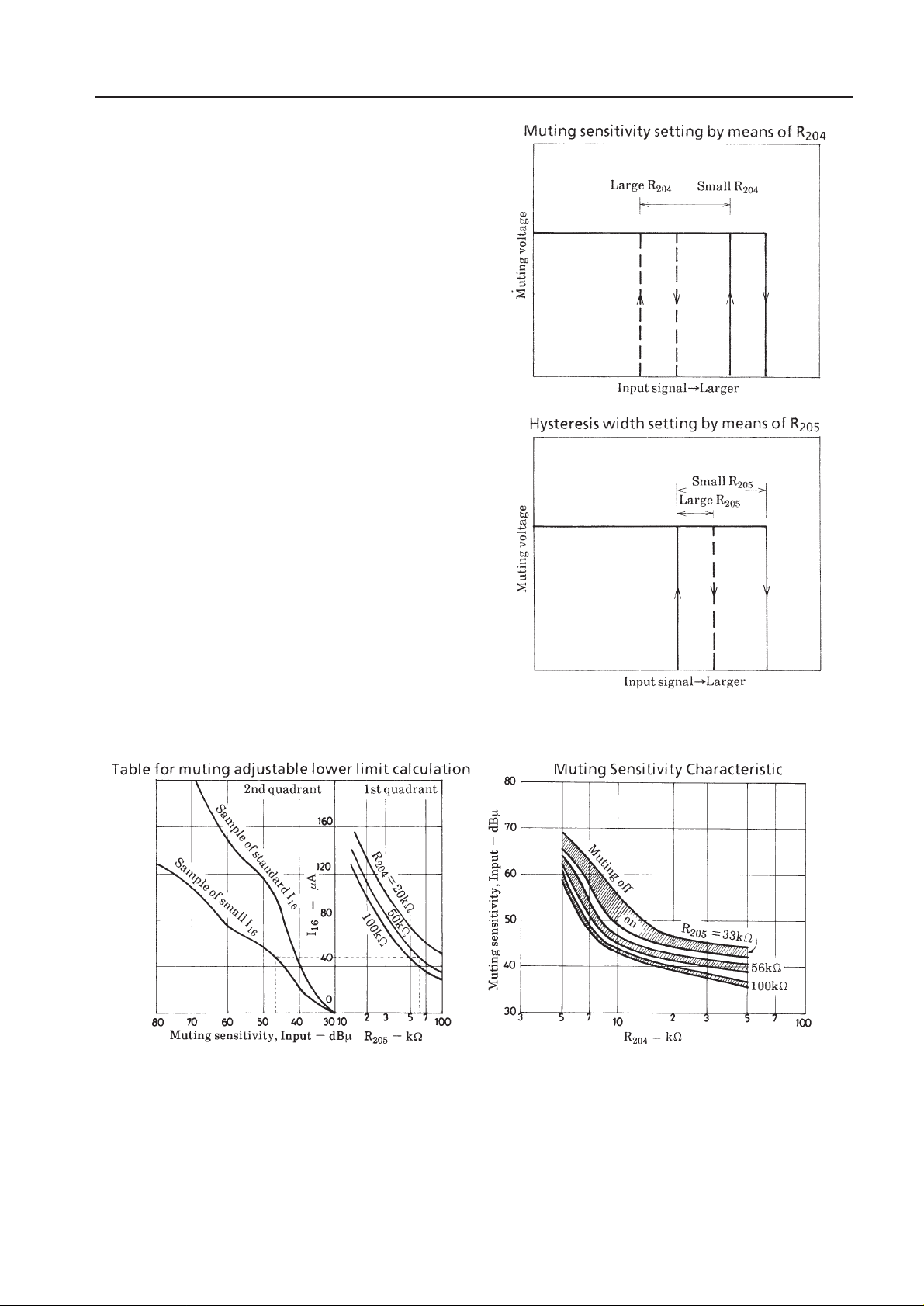
• Setting of muting sensitivity, hysteresis width (Refer to the
equivalent circuit block diagram and application circuit).
Muting sensitivity and hysteresis width are set arbitarily by
varying resistors R
204
and R
205
connected to pins 15 and 16,
respectively. Muting sensitivity is set by varying R
204
; and
if R
204
is made larger, muting sensitivity will shift to the
weak signal side. Hysteresis width is set by varying R
205
;
and if R
205
is made larger, hysteresis width will narrow.
Next, how to set muting sensitivity is concretely described as
follows. In case of using R
204
=50kΩ (semifixed resistor)
and R
205
=56kΩ, the upper limit of current I16, 50µ A,
delivered from the signal meter driver at which muting is
turned ON is obtained from the first quadrant of Table for
muting adjustable lower limit calculation. Muting is turned
ON at I16≤50µ A. If I16≤50µ A, muting is already turned ON
at a point of input being stronger than the setting input and it
is impossible to adjust muting at the setting input. Therefore,
I16>50µ A is required at the setting input. The input at which
a sample with a small I16output meets 50µ A is obtained as
VIN=47dBµ . This input is the maximum value of muting
sensitivity, that is to say, the lower limit at with muting can
be set. The data for sample with a Small I16shown in this
Table is colose to the minimum value, but since samples
with values less than this munimum value may occur, a
margin of some dBµ must be allowed. From the above, the
minimum value for muting setting (muting ON input)
becomes 50dBµ for R
204
(semifixed resistor)=50kΩ and
R
205
=56kΩ.
Page 5
LA1235
No.873-5/12
• Setting of muting circuit constnats
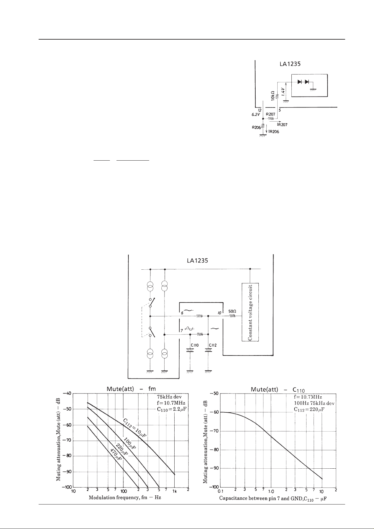
Drive current to be output at muting drive output pin 12 is 0.75mA typ., but
approximately 0.4mA may be caused by variations in characteristic or
changes in temperature (smaller at higher temperatures). It is desirable to
design the circuit so that the total current to be output from pin 12 at the time
of muting ON does not exceed 0.35mA. When driving the muting circuit of
the LA1235, the muting drive current (input current at pin 5) must be
considered besides this total output current. The muting drive current of the
LA1235 is 0.2mA max.
Thus, the muting constants are obrained as follows. If the muting drive
current is I
R207
≥0.2mA, R
207
≤14kΩ occurs and the total current It is shown
by the following expression.
If R
207
=10kΩ is taken with the variation s in voltage V12at pin 12 and input resistance 10kΩ at pin 5 considered,
R
206
≈56.4kΩ is obtained, and then R
206
=68kΩ and R
207
=10kΩ are obtained.
• Setting of C
112
(Capacitance between pin 12 and ground)
C
112
influences S/N and muting attenuation. S/N is improved 0.5 to 2.0dB by changing C
112
from 1µ F to 100µF.
Muting attenuation becomes as shown in Mute (att) – fm (next page) characteristic. This phenomenon occurs
because the output at pin 7 appears at pin 6 through pin 10 and capacitance C
110
between pin 7 and ground also exerts
influence. The relation between muting attenuation andC
110
is such that if C
110
=2.2µ F and C
112
=220µ F, attenuation
at modulation frequency 100Hz becomes –80dB.
AF Output Circuit
It=I
R206+IR207
= +
6.2V
R
206
4.8V
R
206
+10kΩ
(10kΩ : Input resistance at pin 5, Refer to the above figure.)
Muting Circuit
Page 6
LA1235
No.873-6/12
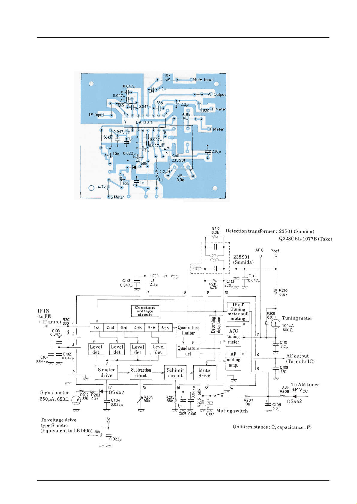
Sample Printed Circuit Pattern
Equivalent Circuit Block Diagram and Sample Application Circuit
(Cu-coated area 70×60mm2)
Page 7

LA1235
No.873-7/12
Description of external parts
Part
No.
R201 Input resistance (Rg)
R202
R203
R204
R205
S meter adjust
Muting sensitivity adjust
Hysterisis adjunt Large hysteresis. Small hysteresis.
Current drain increases.
(Observe max. rating).
Muting sensitivity shifts to weak input
side.
R206
Muting drive circuit load Insufficient drive of detuning muting. When driveing muting of LA3390
(MPX), make less than 200kΩ to
prevent malfunction.
R207
Muting time constant
Abnormal detuning muting
attenuation waveform and abnormal
sound at the time of low frequency
modulation.
Muting response delay.
R208
IF-off voltage applying
resistnace
Large flow-in current at pin 5
(Observe max. rating).
IF-off does not occur.
(IF-off voltage≥7.5V).
R209
R210
AFC, detuning muting
band width, tuning meter
deflection adjust
Large detuning muting bandwidth. Small detuning muting bandwidth.
R211 Detection coil damping Small detection output.
R212
S curve linearity
correction
Find such a value as to cause minimum distortion (THD).
C101
C102
C103
IF amplifier bypass Unstable IF amplifier.
C104 S meter output bypass IF system may be unstable.
C105
C106
Muting drive output
bypass
If low frequency AM compoent is
generated in IF signal, weak signal
muting flutters.
Muting response delay.
C107
C108
Muting drive output
smooth
Abnormal detuning muting
attenuation waveform and abnormal
sound at the time of low frequency
modulation.
Muting response delay.
C109
AF output LPF Unstable IF system. With MPX connected, separation
worsens.
C110
AFC output LPF Muting attenuation worsens and
detuning muting bandwidth narrows.
Detunig muting response delay.
C111
C112
Constant voltage circuit
smooth
S/N, muting attenuation worsen.
C113 Power supply bypass Unstable IF system.
L1 Power supply choke Unstable IF system.
Large detection output.
S meter pointer is off zero point.
(In case of voltage drive type).
Function
Effect
If decreased
Causes matching wigh circuit of preceding stage.
If increased
Proper cares in using IC
• Connect the ground side of bypass capacitors of pins 2, 3 to an area close to pin 4.
• Connect the ground side of bypass capacitors of pins 6, 7, 10, 13, 16 to an area close to pin 14.
• Use the shortest possible wires for detection coil-to-pins 8, 9, 10 connection.
• Pin 13, being used for signal meter drive output, can be also used multipath detection because IF signal envelope
detected is output at this pin.
Page 8
LA1235
No.873-8/12
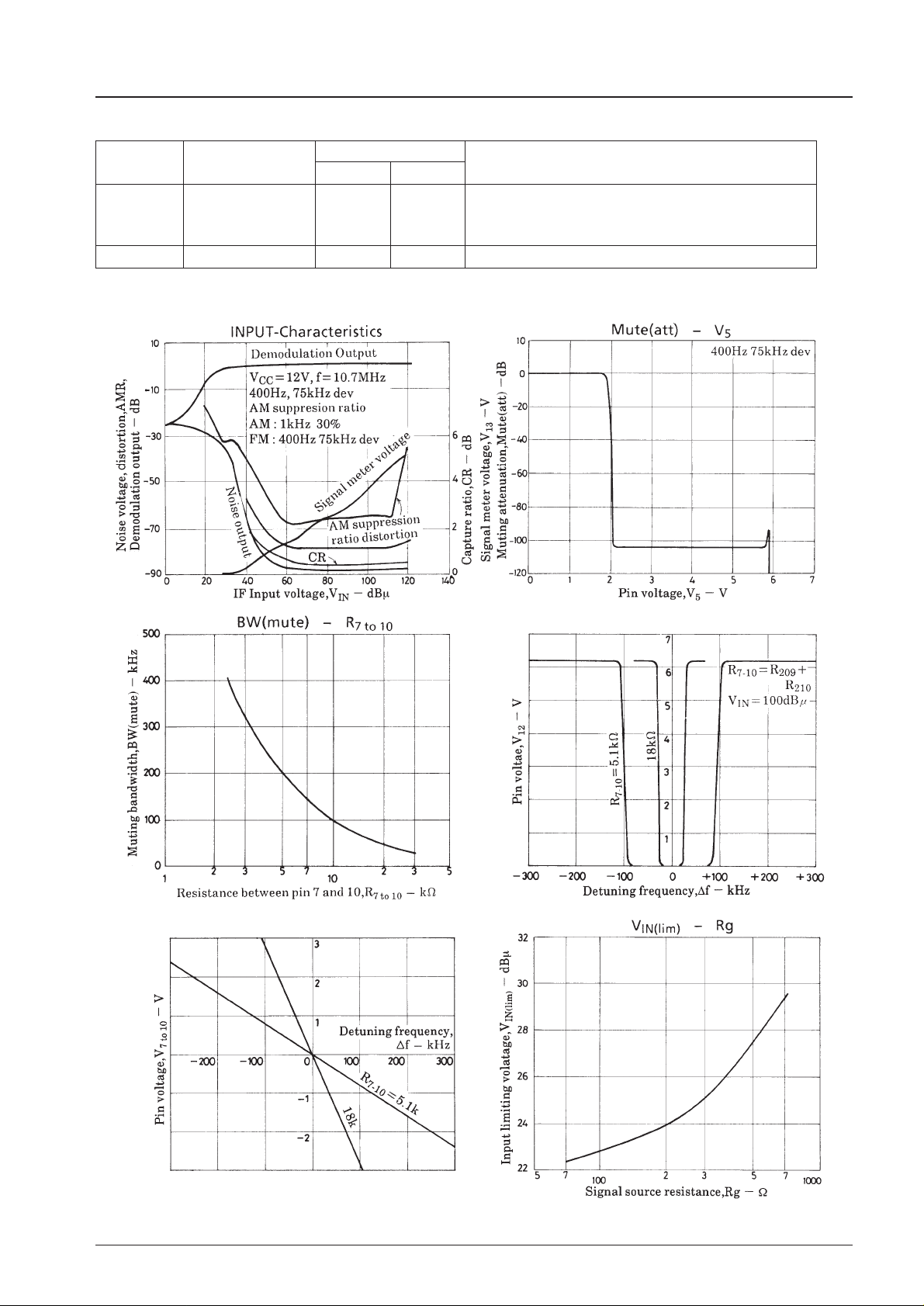
Coil specifications
Supplier
Sumida
Coil name
235S01
SNY-074-1919A
Damping resistance
Remarks
Containing fixed inductance 26µF.
Containing fixed inductance 26µF.
(Improvement in temperature characteristic).
R211 R212
4.7kΩ
7.5kΩ
3.3kΩ
2.4kΩ
Toko Q228CEL-1077B Containing fixed inductance13kΩ 3.0kΩ
V12– ∆f
V
7 to 10
– ∆f
Page 9
LA1235
No.873-9/12
Page 10
LA1235
No.873-10/12
Page 11
LA1235
No.873-11/12
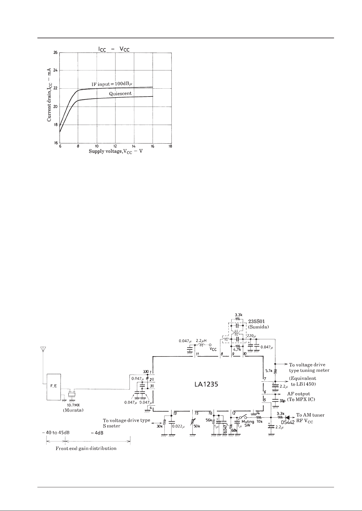
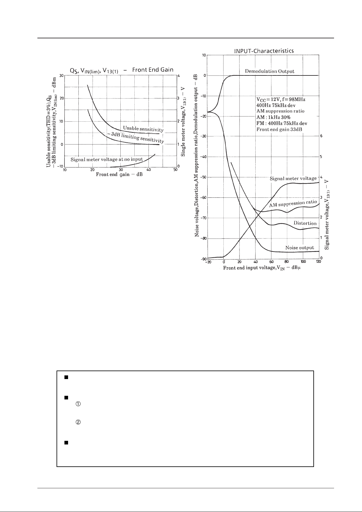
Cain distribution of application circuit
If IC anone is operated without front end, the tuning meter deflects toward plus side at the time of no input. This
phenomenon is caused by the fact that the noise component to be applied to the quadrature multiplication circuit is not
syummetric with respect to 10.7MHz but is shifted toward lower frequency side because the frequency characteristic of
IF amplifier attenuates at high frequencies and the phase shift circuit is of low-pass type. If the formt end is attached and
the noise which passes through the narrowband filter of IF stage and spreads symmetrically with respect to 10.7MHz is
stronger than the noise generated inside the IC, the tuning meter reads 0.As the gain of the front end is decreased, input
limiting sensitivity and usable sensitivity worsen abruptly. This phenomenon is caused by the fact that since the tuning
meter is set to 0 at the time of no input the tuning point of the quadrature circuit must be shifted toward lower frequency
side than 10.7MHz and the demodulation output waveform is deformed asymmetrically at an input in the vicinity of
usable sensitivity. However, if the gain of the front end is too increased, the signal meter poiter does not return to zero
point at the time of no signal.
Sample Application Circuit
Unit (resistance : Ω, capacitance : F)
Page 12
LA1235
No.873-12/12
No products described or contained herein are intended for use in surgical implants, life-support systems,
aerospace equipment, nuclear power control systems, vehicles, disaster/crime-prevention equipment and
the like, the failure of which may directly or indirectly cause injury, death or property lose.
Anyone purchasing any products described or contained herein for an above-mentioned use shall:
Accept full responsibility and indemnify and defend SANYO ELECTRIC CO., LTD., its affiliates,
subsidiaries and distributors and all their officers and employees, jointly and severally, against any
and all claims and litigation and all damages, cost and expenses associated with such use:
Not impose any responsibilty for any fault or negligence which may be cited in any such claim or
litigation on SANYO ELECTRIC CO., LTD., its affiliates, subsidiaries and distributors or any of
their officers and employees jointly or severally.
Information (including circuit diagrams and circuit parameters) herein is for example only; it is not guaranteed for volume production. SANYO believes information herein is accurate and reliable, but no guarantees
are made or implied regarding its use or any infringements of intellectual property rights or other rights of
third parties.
This catalog provides information as of October, 1997. Specifications and information herein are subject
to change without notice.
 Loading...