

Page 1
LA1245
Ordering number : EN737F
AM Electronic Tuner
Monolithic Linear IC
SANYO Electric Co.,Ltd. Semiconductor Bussiness Headquarters
TOKYO OFFICE Tokyo Bldg., 1-10, 1 Chome, Ueno, Taito-ku, TOKYO, 110 JAPAN
63097HA (KOTO)/33194HO/N050JK/8044KI,TS3173KI/O020KI No.737-1/11
Overview
LA1245 is a high performance IC to be used as an AM
electronic tuner. It provides an automatic search-stop
signal, local oscillator buffer-output, and the low level
local oscillation, as well as providing all other functions
required of an AM tuner. Moreover, the stable local
oscillation from LW to SW facilitates the use of many
band.
Functions
• RF amplifier • MIX • OSC (with ALC) • Detection
• IF amplifier • AGC • Local oscillation buffer-output
• Signal meter driving output (also used as an automatic
search stop-signal)
• etc.
Package Dimensions
unit : mm
3021B-DIP20S
[LA1245]
SANYO: DIP20S
Features
• Narrow-band signal meter : Available as an automatic search-stop signal (also available as a wide-band signal
meter). Signal meter output=1/2 frequency ±1.5kHz typ.
• Local oscillation buffer-output : Facilitates the design of electronic tuning systems and frequency representation.
• OSC (with ALC) : The oscillation output is stabilized at a low level (350 mVrms) for a varactor
diode, and tracking error is minimized.
• RF amplifier : Excellent in usable sensitivity by incorporating low-noise transistors in cascode
circuit (45dB/m typ).
• MIX : Double balanced differential MIX prevents the influence of spurious radiation and
IF interferences (IF interference = 85dB typ).
• Low noise : Excellent in S/N for intermediate input (57dB typ).
• Compensation for VCCfluctuation : Allows little gain fluctuation and little distoriton fluctuation (8 to 16 V).
• Low shock noise : Able to decrease the shock noise by selecting AGC time constant when changing
VCC-on and/or switching the mode.
Page 2
Specifications
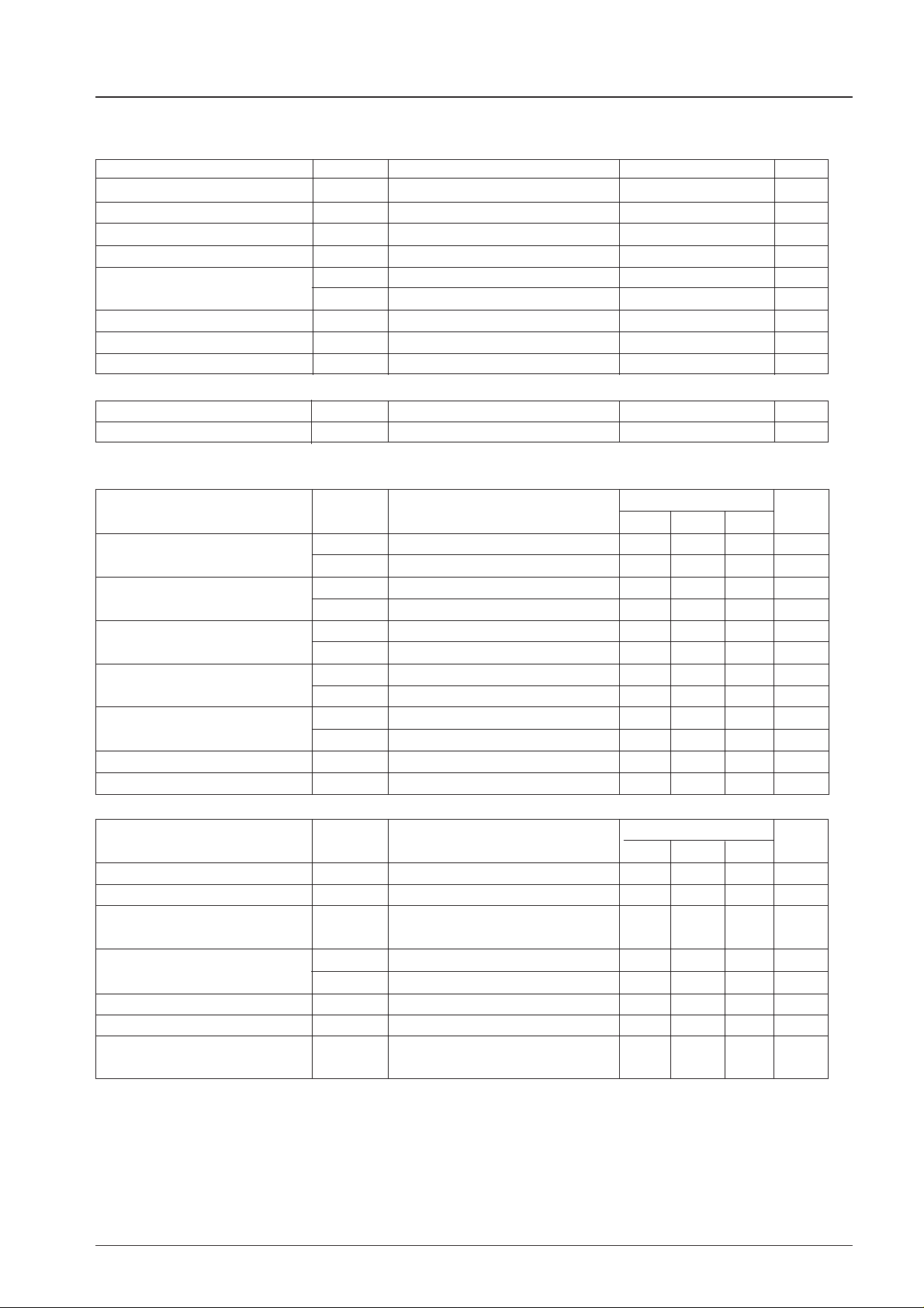
Maximum Ratings
at Ta=25°C
Parameter Symbol Conditions Ratings Unit
Supply voltage V
CC
max Pin 8, 14 16 V
Output voltage V
o
Pin 5, 7 24 V
Input voltage V
I
Pin 3 5.6 V
Supply current I
CC
max Pin 5+7+8+14 32 mA
Output high drive current I
18
Pin 18 5 mA
I
20
Pin 20 2 mA
Allowable power dissipation Pd max See Figure 2 700 mA
Operating temperature Topr –20 to +70 °C
Storage temperature Tstg –40 to +125 °C
Recommended Operating Conditions at Ta=25°C
Parameter Symbol Conditions Ratings Unit
Recommended supply voltage V
CC
12 V
Operating Characteristics at Ta=25°C, V
CC
=12V, fr=1MHz, fm=400Hz, at specified test circuit
(based on application circuit).
Parameter Symbol Conditions
Ratings
min typ max
Unit
Current drain I
CC
1 quiescent 16.0 25.0 35.0 mA
I
CC
2 107 dBµ input 19.0 29.0 40.0 mA
Detection output Vo1 23 dBµ input, mod. 30% –27.5 –23.0 –18.5 dBm
Vo2 80 dBµ input, mod. 30% –15.5 –12.5 –9.5 dBm
Signal to noise ratio S/N1 23 dBµ input, mod. 30% 16 20 dB
S/N2 80 dBµ input, mod. 30% 52 57 dB
Total harmonic distortion THD1 80 dBµ input, mod. 30% 0.4 1.0 %
THD2 107 dBµ input, mod. 30% 0.3 1.0 %
Signal meter output V
SM
1 quiescent 0 0.5 V
V
SM
3 107 dBµ input 3.0 4.5 7.0 V
Input at signal meter output=1V V
IN
1 VSMoutput=1V 19.0 25.0 31.0 dBµ
Local oscillation-buffer output V
osc
250 350 mVrms
Reference Characteristics
Parameter Symbol Conditions
Ratings
min typ max
Unit
Signal meter output V
SM
2 40 dBµ input 2.5 V
Total harmonic distortion THD3 112 dBµ input, mod.30% 2 %
Local oscillation fluctuation ∆V
osc
V
osc
L (522kHz) to V
osc
H 10 mVrms
within a band (1647kHz)
Signal meter band width* V
SM-BW1
80 dBµ input, 1/2 output frequency ±1.5 kHz
V
SM-BW2
80 dBµ input, 1/10 output frequency
–4.5/+7
kHz
Selectivity ±10kHz at 30% mod. 45 dB
IF interference fr=600kHz 85 dB
Image frequency interference fr=1400kHz 40 dB
ratio
* BFB450C4 N (Murata, Co.,) was used as a narrow band filter.
(Note) 0 dBm=775mV, 0 dBu=1µV.
LA1245
No.737-2/11
Page 3
LA1245
No.737-3/11
Using the automatic search-stop signal
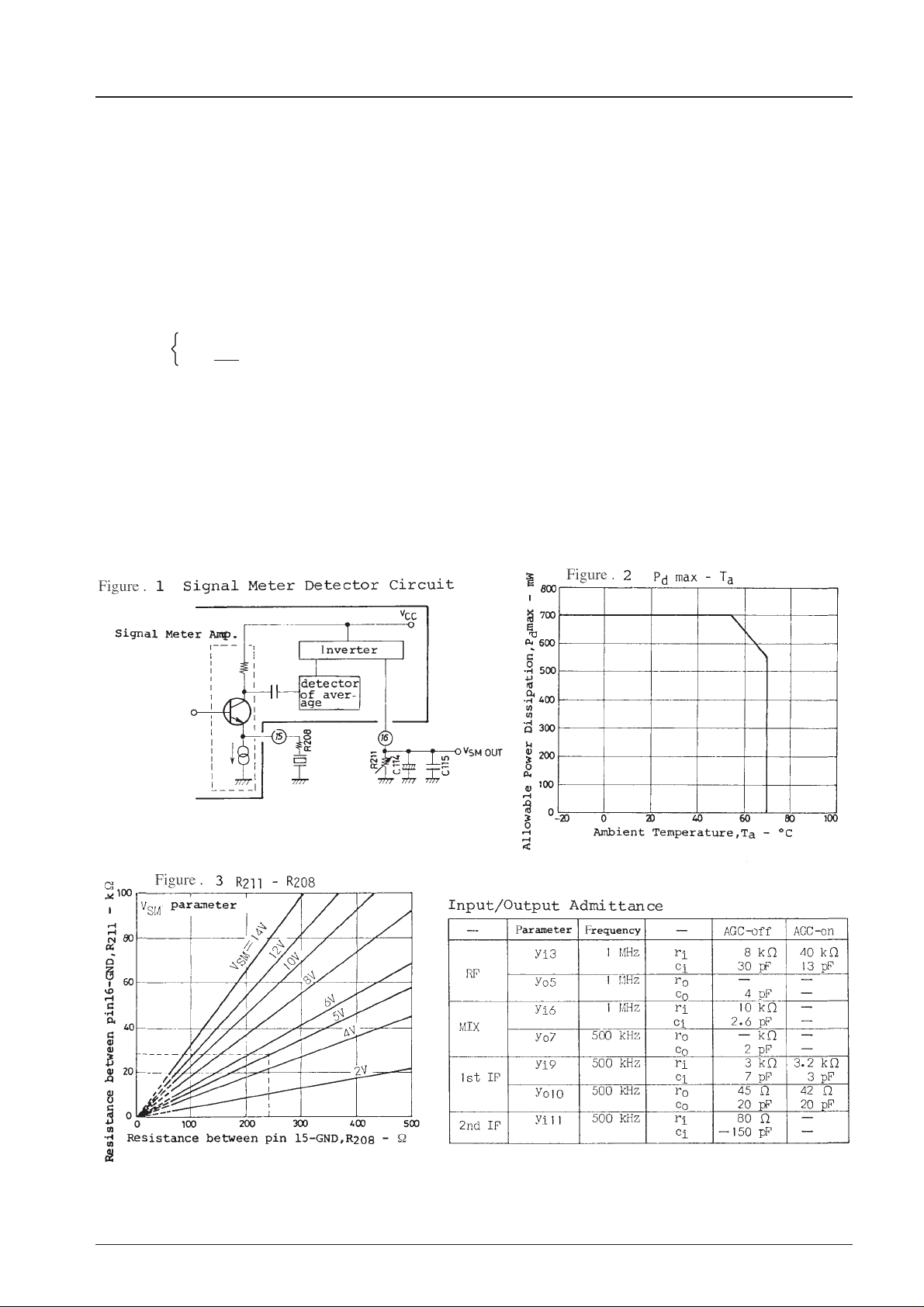
Signal Meter-driving output circuit is equivalent to Figure. 1, signal meter driving output (abbreviated as VSM) is
narrowed in band width and can be used as an automatic search-stop signal when a narrow band series resonator is
connected to pin 15. VSMcan be adjusted with R
208
and R
211
both in wide band and narrow band since R
208
is
inversely proportional to VSM, while R
211
is proportional to VSM. R
208
is related to the Q of narrow band signal
meter. When the resistance of R
208
is increased, the Q will be damped and the band width increased. On the other
hand, R
211
used as the output impeadance of VSMand affects the cut-off frequency and time constant of low pass
filter for VSMand the meter drive impedance. The time constant τ and the cut-off frequency fc can be expressed as
follows :
τ = (C
114+C115+CS
) (R
211
//Rin)
fc =
2πτ
1
A semi-fixed resistor is recommended to be used as R
211
to cope with the fluctuation of VSM. Refer to Figure. 3 for
the value of the semi-fixed resistor since this depends upon VSMand R
208
. Figure. 3 shows the lowest limit of the
semi-fixed resistor in relation to R
208
with the parameter of VSMset point, and the value of the semi-fixed resistor
will be equal to or greater than that shown in Figure. 3. For example, when VSM=5V and R
208
=240Ω, R
211
becomes
28kΩ. Thus, the value of the semi-fixed resistor is determined to be about 30kΩ. When the value of VSMis too large,
it is limited and saturated to the source voltage so it is recommended to follow the condition of VSM≤VCC–2(V).
When a narrow band serial resonator is used, include the resonant impedance to determine the value of R
208
.
Page 4
LA1245
No.737-4/11
Notes on LA1245 usage
1. When suddenly tuned to a broadcasting station of intermediate or high field strength, a large current of high frequency
flows into the signal meter circuit, causing the local oscillator malfunctions and abnormal noises.
To eliminate this :
· Use R
208
≥240Ω for manual tuning type.
· Use R
208
≥82Ω, and use the local oscillation coil at the 1/3 tap (except SW) for electronic tuning type (which uses a
narrow band filter).
2. Use the bias on the condition RF VCC≤IF VCC, since abnormal noise levels might be caused when detuning a strong
input on the codition RF VCC>IF VCC.
3. Use the signal meter driving output (VSM) at VSM≤VCC–2 (V) to avoid saturation caused by VCC.
4. Use 1/2 or more tap of LW and MW oscillation coil to improve S/N and the detuning characteristics of the distortion
ratio.
5. Use the full-tap of SW oscillation coil, to allow the sag in oscillation power by the decreasing of Q.
6. Avoid the coupling of the antenna tuning circuit and the local oscillating circuit so as not to leak the local oscillation
into the antenna tuning circuit.
7. Connect the detection capacitor C
113
between pin 13 (output) and pin 14 (VCC) to avoid the leakage of the IF signal
into the GND line. Connection between pin 13 and pin 12 (GND) increases the tweet interference and deteriorates the
usable sensitivity.
Moreover, depending on the positions of C
113
and the bar antenna, higher harmonics having twice or three times the
frequency of the IF signal may pass into the antenna and cause tweet interference, and in extreme cases oscillation
might be cause. To prevent this :
· Shorter lead wires and connect them near 13 and 14 pins.
· Place C
113
far from the antenna.
Page 5
LA1245
No.737-5/11
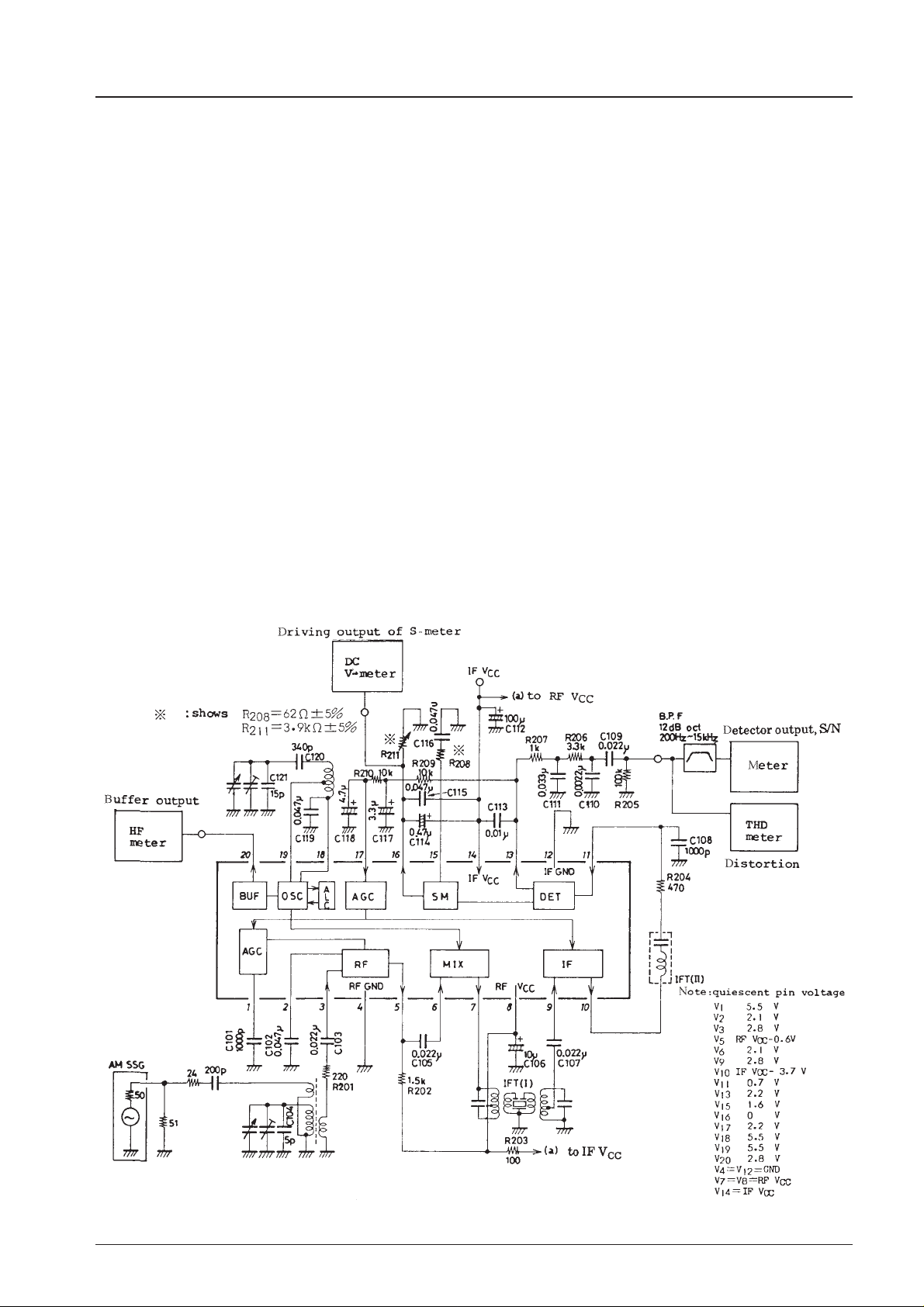
8. When a cable or something similar is connected to a local oscillation buffer (pin 20), which is equivalent to
connecting a capacitor of about 20pF, the output from the buffer will be of sawtooth waves, causing the level low at
the short wave band. To prevent this, connect a resistor between pin 20 and GND, which will increase the operating
current of the buffer amplifier. Since the maximum current obtained from pin 20 is 2mA, the suitable resistance
between pin 20 and GND is 1.5kΩ.
9. Use a semi-fixed resistor for R
211
to allow the fluctuation of VSM.
10. When changing an IFT or using an RF tuner, select a filter and related circuits according to the following conditions.
The input levels of each terminal where 30% modulated detection output of –25dBm is obtained are as follows :
Pin 11 input when Rg=520Ω (470Ω+ 50Ω) 75dBµ
Pin 9 input when Rg=50Ω 53dBµ
Pin 6 input when Rg=50Ω 48dBµ
Pin 3 input when Rg=50Ω 22dBµ
Slight change in IFT, however, will be covered by changing the constant of resistors R
202
and R
204
.
11. When the coupling coefficient of the local oscillation coil is small and an anti-resonance point of about 100MHz is
present or the stray capacitance between pin 19 and pin 20 is large, the buffer output (pin 20) may be subject to
parasitic oscillation of about 100MHz. In this case, connect a capacitor of about 30pF between pin 20 and GND. To
observe parasitic oscillation, connect a capacitor of 5pF in series with the probe. If the probe is connected direct to
pin 20, the input capacitance of the probe causes parasitic oscillation to stop, which makes it impossible to observe.
Sample Application Circuit 1
Unit (resistance : Ω, capacitance : F)
Page 6
LA1245
No.737-6/11
Page 7
LA1245
No.737-7/11
Page 8
LA1245
No.737-8/11
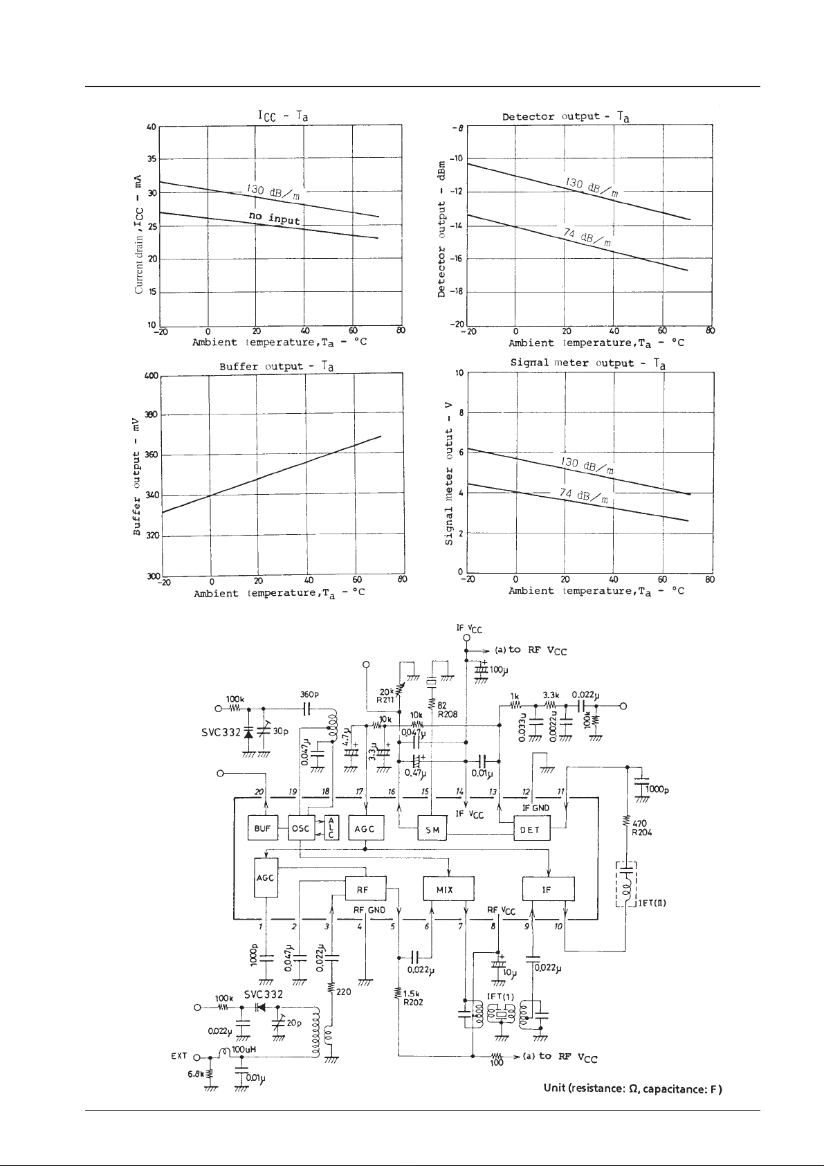
Sample Application Circuit 2 : Using variable capacitance diodes
Page 9
LA1245
No.737-9/11
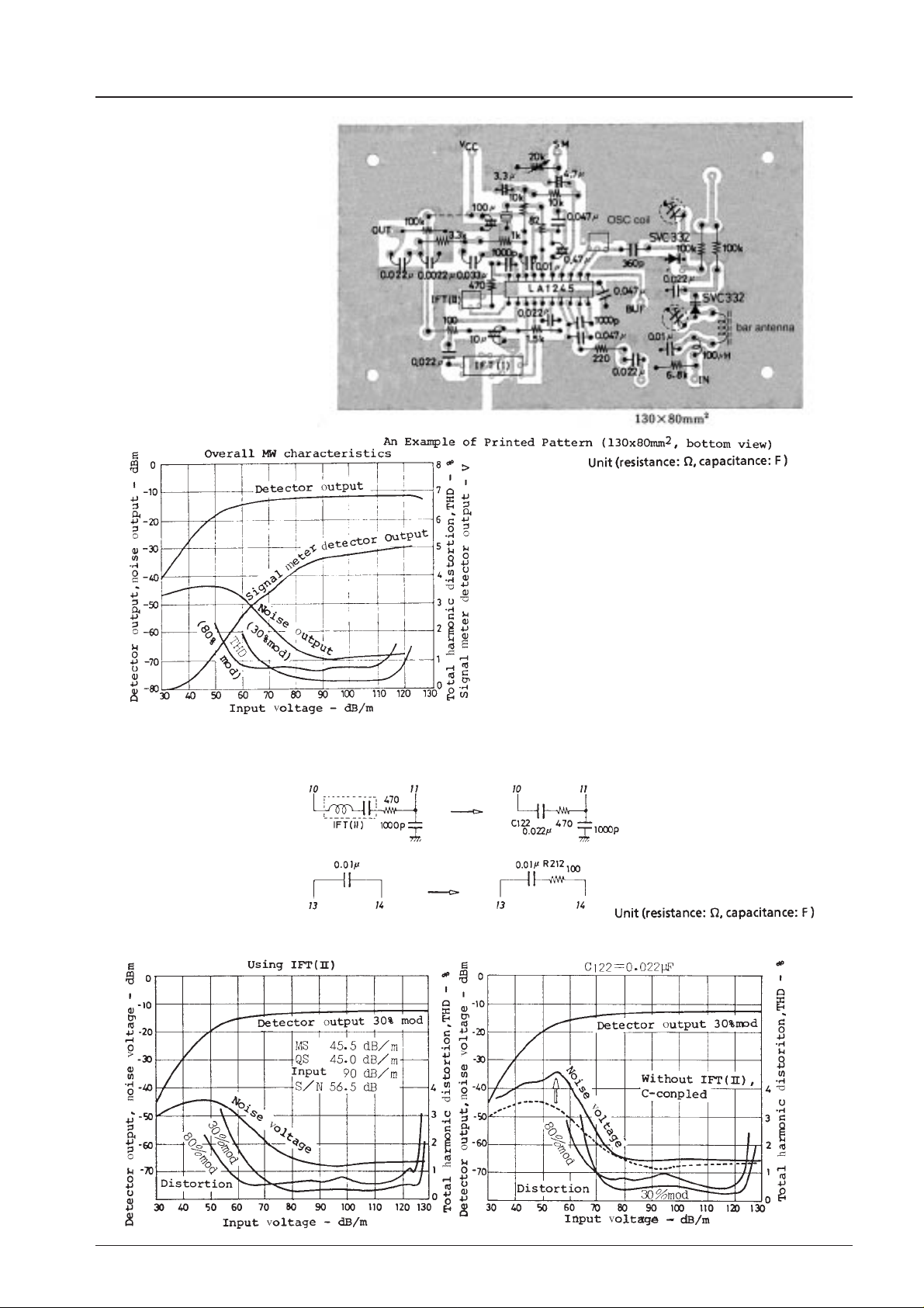
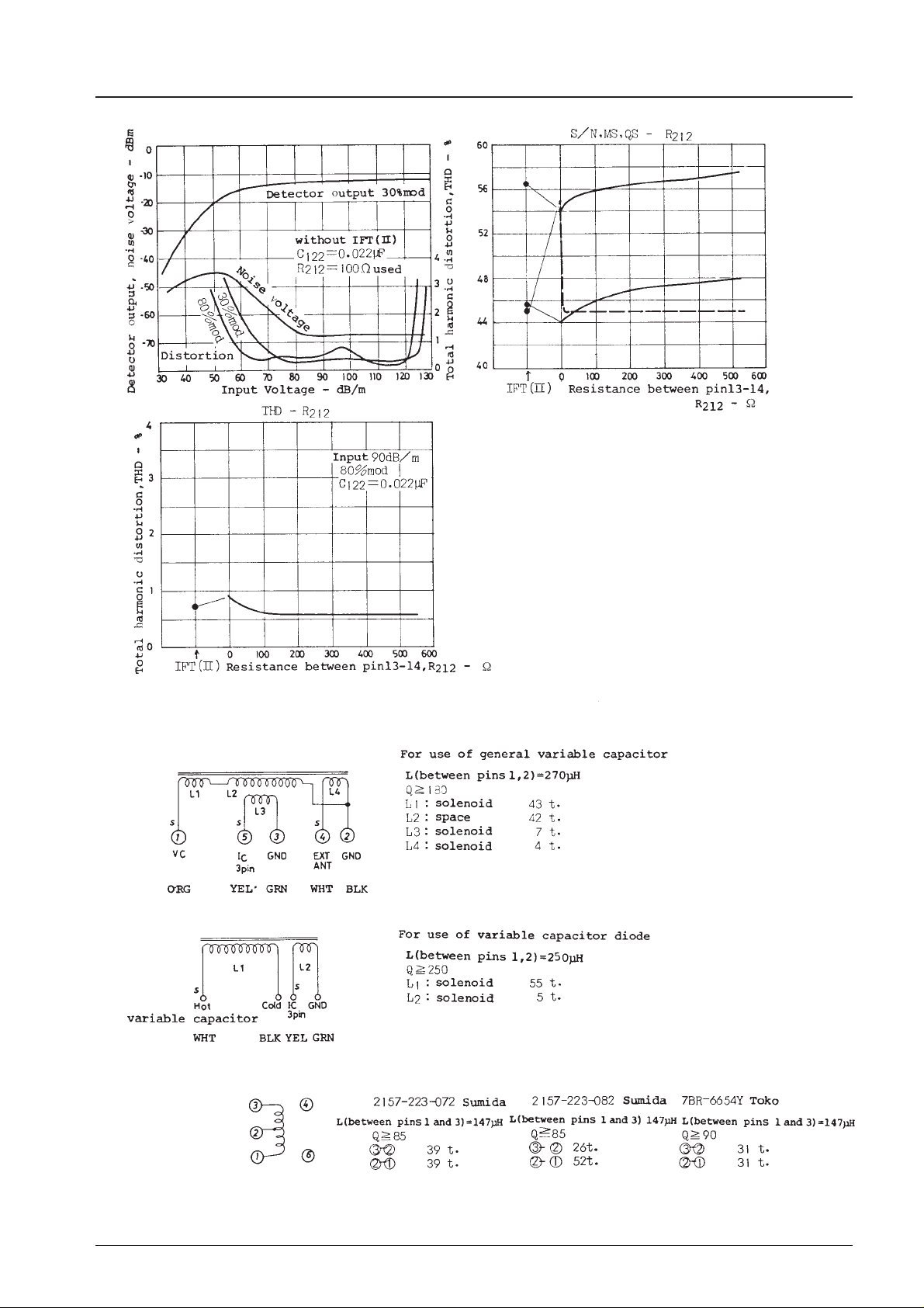
Sample Application Circuit 3 : Rejecting IFT (II)
Following 2 changes are recommended as C-conpling without IFT (II)
Comparison of characteristics varying parts.
Page 10
LA1245
No.737-10/11
Peripheral Parts
(1) Bar Antenna (34H-052-869 Sumida Co.,)
(2) Bar Antenna (C-4698 Coil Snake Co.,)
(3) Osc coil
Page 11
LA1245
No.737-11/11
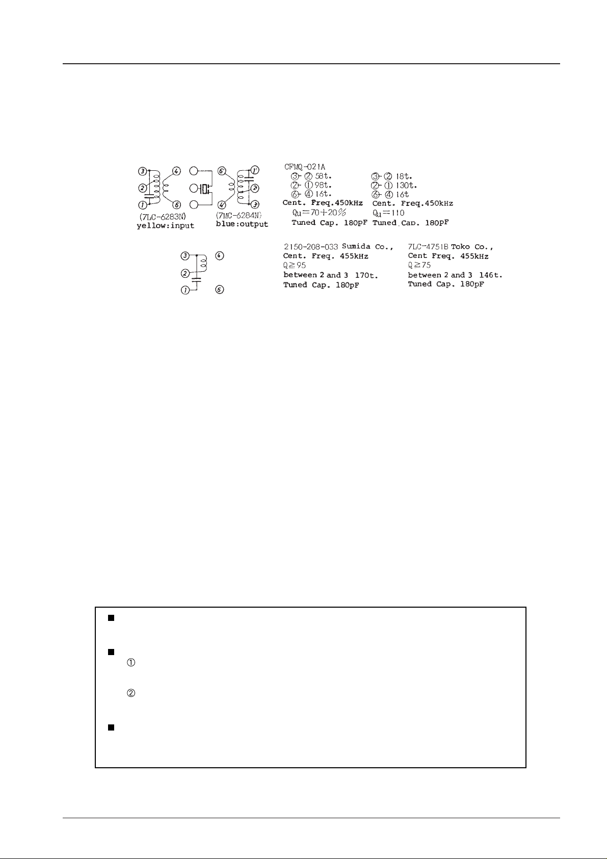
(4) Variable Capacitor (C123A Alps Co.,)
c max 326.8 pF
c min 6.7 pF
(5) Variable Capacitor Diode (SVC332 Sanyo)
(8) Narrow Band Resonator (BFB450C4 N Murata Co.,)
(6) IFT (I) (CMFQ-021A Toko Co.,)
(7) IFT (II)
No products described or contained herein are intended for use in surgical implants, life-support systems,
aerospace equipment, nuclear power control systems, vehicles, disaster/crime-prevention equipment and
the like, the failure of which may directly or indirectly cause injury, death or property lose.
Anyone purchasing any products described or contained herein for an above-mentioned use shall:
Accept full responsibility and indemnify and defend SANYO ELECTRIC CO., LTD., its affiliates,
subsidiaries and distributors and all their officers and employees, jointly and severally, against any
and all claims and litigation and all damages, cost and expenses associated with such use:
Not impose any responsibilty for any fault or negligence which may be cited in any such claim or
litigation on SANYO ELECTRIC CO., LTD., its affiliates, subsidiaries and distributors or any of
their officers and employees jointly or severally.
Information (including circuit diagrams and circuit parameters) herein is for example only; it is not guaranteed for volume production. SANYO believes information herein is accurate and reliable, but no guarantees
are made or implied regarding its use or any infringements of intellectual property rights or other rights of
third parties.
This catalog provides information as of June, 1997. Specifications and information herein are subject to
change without notice.
 Loading...