

Page 1
LA1143
Ordering number : EN1140D
FM IF System for Car Radios
Monolithic Linear IC
SANYO Electric Co.,Ltd. Semiconductor Bussiness Headquarters
TOKYO OFFICE Tokyo Bldg., 1-10, 1 Chome, Ueno, Taito-ku, TOKYO, 110 JAPAN
91297HA (KT)/D157KI/2126KI/5085MW/D142KI, TS No.1140-1/5
Overview
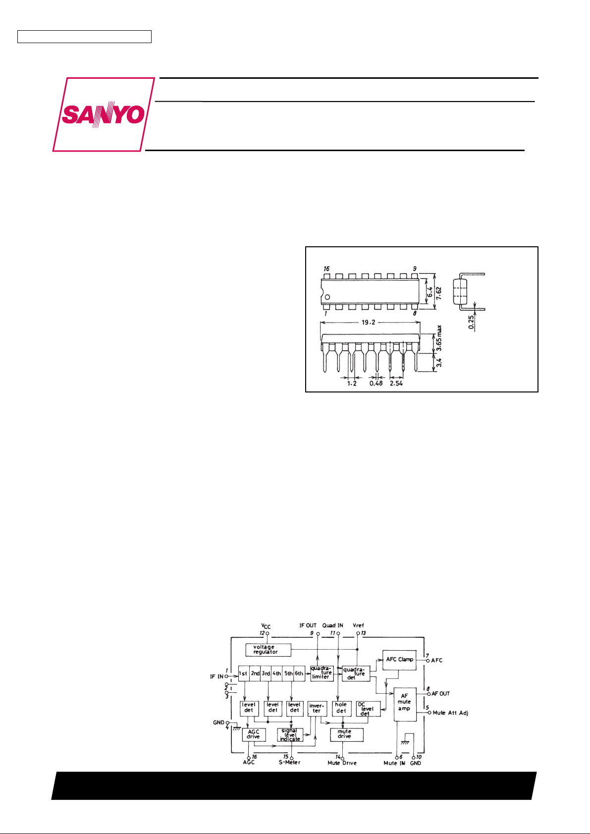
The LA1143 is an IF system IC designed for FM car stereo
receivers. It features versatile muting characteristics and
allows receiver designers to realize the muting
performance according to their design concept. Since the
muting characteristics can be varied with a switch or a
semi-fixed resistor, DX-Local switching will be
accomplished with ease.
Functions
• IF amplification/limiter • Quadrature detector
• AF preamplifier • AFC output
• Signal meter output • AGC output
• Muting at detuning • Muting at small input
Package Dimensions
unit: mm
3006B-DIP16
[LA1143]
SANYO: DIP16
Features
1. Versatile mutings
a) When muting operation is performed under a weak signal strength, an attenuation slope of the audio output against
the input signal strength variations can be set at any given value.
b) Maximum muting attenuation can be selected to be approximately 6 to 40dB.
c) Input signal strength level which actuates the muting circuit can be set freely.
2. High limiting sensitivity (25 dBµ typ. with muting off) provides a good quieting characteristic.
3. High S/N (78dB typ.)
4. Low distortion (0.05% typ.) available, if used with double-tuned circuits.
5. Good AMR (63dB with 6 stages of differential IF amplifiers).
6. Signal meter drive output proportional to the input signal strength in dB (suitable to control multiplex IC LA3373).
7. Clamped (±VBE) AFC output, bandwidth adjustable.
8. Delayed AGC output for front end circuit.
Equivalent Circuit Block Diagram
Page 2
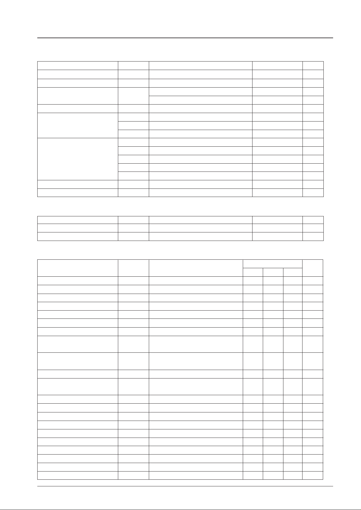
Specifications
Maximum Ratings
at Ta=25°C
Parameter Symbol Conditions Ratings Unit
Maximum supply voltage V
CC
max Pin 12 16 V
Maximum supply current I
CC
max Pin 12 40 mA
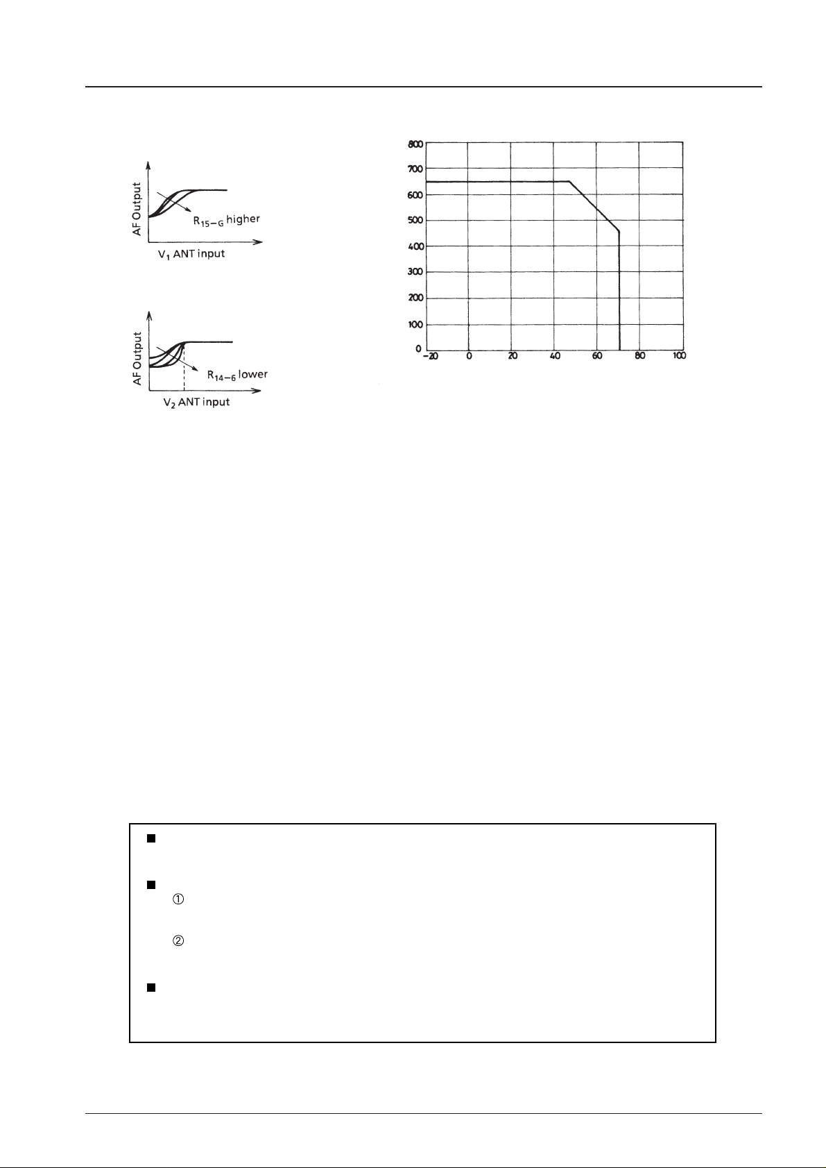
Allowable power dissipation Pd max Ta=25°C 640 mW
Ta=70°C 460 mW
Input voltage V
IN
Pin 1 to 2 ±1 Vp-p
Flow-in current I
2
Pin 2 ±0.2 mA
I
3
Pin 3 ±0.2 mA
I
6
Pin 6 2 mA
Flow-out current I
5
Pin 5 1 mA
I
13
Pin 13 2 mA
I
14
Pin 14 2 mA
I
15
Pin 15 1 mA
I
16
Pin 16 1 mA
Operating temperature Topr –20 to +70 °C
Storage temperature Tstg –40 to +125 °C
Operating Condition at Ta=25°C
Parameter Symbol Conditions Ratings Unit
Recommended supply voltage V
CC
8 V
Operating voltage range V
CC
op 7.5 to 16 V
Operating Characteristics at Ta=25°C, V
CC
=8V, f=10.7MHz, See specified Test Circuit.
Parameter Symbol Conditions
Ratings
min typ max
Unit
Quiescent current I
CCO
Quiescent 15 21 27 mA
Current drain I
CC
VIN=100dBµ 20 25 30 mA
Demodulation output V
O
VIN=100dBµ,400Hz, 100% mod. 200 260 320 mVrms
Total harmonic distortion THD V
IN
=100dBµ,400Hz, 100% mod. 0.05 0.2 %
Signal to noise ratio S/N V
IN
=100dBµ,400Hz, 100% mod. 72 78 dB
Input limiting voltage V
IN
(lim) VO: 3dB down, 400Hz 100% mod. 25 29 dBµ
Muting sensitivity V
IN
(mute) V14=2.0V 22 26 35 dBµ
Muting attenuation (1) Mute(ACC) V
6
=2.0V (22kΩ), VIN=100dBµ, 10 15 20 dB
400Hz 100% mod.
Muting attenuation (2) Mute(ACC) V
6
=5.0V (22kΩ), VIN=100dBµ, 24 28 32 dB
400Hz 100% mod.
Muting bandwidth BW(mute) V
IN
=100dBµ, V14=2.0V 140 210 370 kHz
AM rejection ratio AMR V
IN
=100dBµ, FM 400Hz 100% mod. 50 63 dB
AM 1kHz 30% mod.
Muting drive output V
14-0
Quiescent 3.5 4.2 5.0 V
Muting drive output V
14-100
VIN=100dBµ 0 0 0.3 V
Signal meter output (1) V
15-0
Quiescent 0 0.1 0.3 V
Signal meter output (2) V
15-50
VIN=50dBµ 0.8 1.4 2.0 V
Signal meter output (3) V
15-70
VIN=70dBµ 1.6 2.4 3.2 V
Signal meter output (4) V
15-100
VIN=100dBµ 4.5 5.3 6.0 V
AGC output (1) V
16-0
Quiescent 3.5 4.1 4.5 V
AGC output (2) V
16-100
VIN=100dBµ 0 0.02 0.3 V
Offset voltage (1) V
7-13
Quiescent, pin 7 to 13 –0.25 0 +0.25 V
Offset voltage (2) V
8-13
Quiescent, pin 8 to 13 –0.5 0 +0.5 V
LA1143
No.1140-2/5
Page 3
LA1143
No.1140-3/5
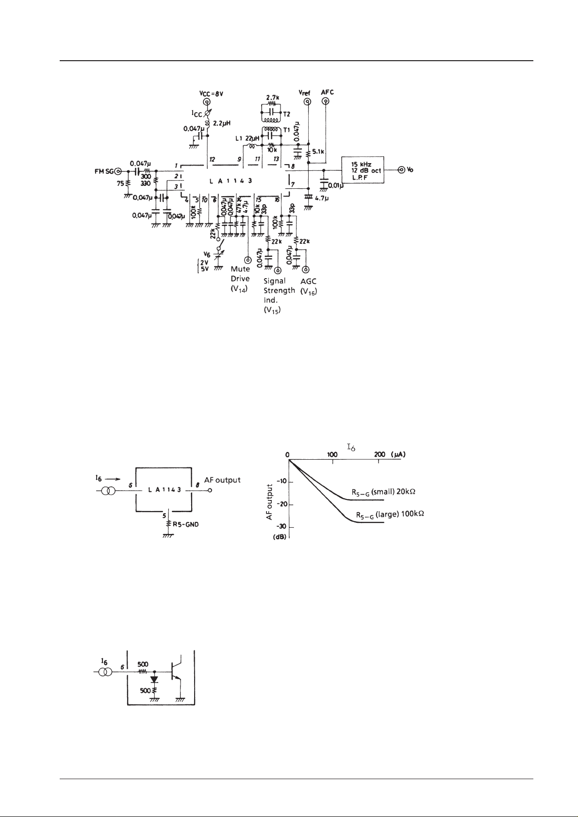
AC Test Circuit
Unit (resistance : Ω, capacitance : F)
Muting Characteristic
The muting operation in the LA1143 is performed by an AF preamplifier, the gain of which varies continuously with
control current, and a muting drive circuit which supplies the control current.
The gain of th AF preamplifier decreases with increasing gain control current applied to pin 6. However, the gain does
not decrease further when the control current reaches approximately 120µA or more. The lower limit of the gain under
this condition depends upon a resistor connected between the pin 5 and GND, and the higher the resistance the lower the
gain (the higher the attenuation). Thus the maximum muting attenuation will be set by connecting the resistor between
the pin 5 and GND.
Since the muting control input pin 6 is connected to the base of the emitter-grounded transistor (through a protection
resistor of 500Ω in series), the voltage between pin 6 and GND is about 0.6V when the control current is applied.
In actual cases, the muting operation is accomplished by applying a voltage drive type muting drive output (pin 14) to
pin 6 through a high resistance (up to 20kΩ).
The muting drive output comes in three types :
1) Hole detector output which develops a voltage when C/N (carrierto-noise ratio) lowers under weak signal input condition.
2) A reversed output of the signal strength indicating output (output
at pin 15).
3) A bandwidth limited muting drive output which develops a
voltage when the AFC output becomes higher than ±VBEduring
detuning operation.
All these outputs are led to an OR circuit and the processed output is
developed at pin 14. Of the above muting drive outputs, descriptions
on the hole detector output and the bandwidth limited muting drive
Continued on next page.
Unit (resistance : Ω)
T1 : CBTKAC-24782AUO (Toko Co.)
T2 : CBTKAE-24783X (Toko Co.)
22µH : S-220J (Korin Co.)
Input signal strength is an actual
input at pin 1.
Page 4
LA1143
No.1140-4/5
Continued from preceding page.
output will be omitted, since they are the same as those used in conventional quadrature detector ICs ( such as LA1230,
LA1231N).
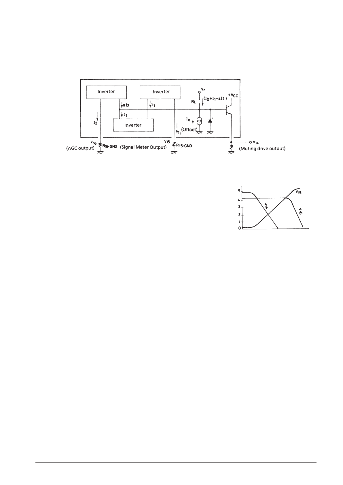
The inverted output of the signal strength indication output is obtained as illustrated below.
By referring to the illustration, V14is given by the formula : V14=Vr–(I0+I1–aI2)RL–VBE.
Conditions are : Vr≈4.9V, I0≈0.2mA, a≈2, RL=22kΩ, VBE≈0.6V, I1=V15/R
15-G
,
I2=V16/R
16-G
, where V16is a constant equal to 4.1V (typ.) for medium or lower
signal input levels, where the muting drive output is required. Since the V
15
increases proportionally to the increase of the input signal strength, I1 will also
increase. Therefore the V14will decrease with increasing signal strength. Thus the
required muting drive output can be obtained by selecting proper values of R
15-G
and R
16-G
.
For example, the muting drive output moves toward strong input signal level if th R
16-G
is decreased, or the muting
drive output becomes zero due to the offset current IOunder a weak signal input condition, if the R
16-G
is increased to
infinity (namely pin 16 is opened). However the muting drive output caused by a hole detector still exists in this case. In
creasing R
15-G
decreases the slope of the curve for the muting drive output vs. antenna signal input level, or decreasing
the R
15-G
increases the slope of the curve. Furthermore, varying the value of a resistor connected between the muting
drive output (pin 14) and the muting control input (pin 6) changes the value of the muting control current required to
obtain the same muting drive output, accordingly a slope of curve for muting attenuation vs. antenna signal input level is
also changed.
These characteristics investigated by using an actual receiver are shown on the curves below. The general method to
adjust the muting circuit of the LA1143 is : to set the signal input level required to actuate the muting circuit with the
R
16-G
, to adjust the slope of the curve for the muting attenuation vs. antenna signal input with the R
15-G
, and to adjust
the maximum muting attenuation (determined by setting the noise level at no signal) with the R
5-G
. The slope of the
curve for the muting attenuation vs. antenna signal input level can also be adjusted by the resistor connected between
pins 14 and 6 in addition to R
15-G
, however, selecting a resistor too high does not allow the muting control current
flowing into pin 6 to reach 120µA even though the maximum muting drive output (V14) is applied, namely the muting
attenuation does not reach its maximum value. Accordingly a recommended value of the resistor between pins 14 and 6
is about 22kΩ.
Page 5
LA1143
No.1140-5/5
No products described or contained herein are intended for use in surgical implants, life-support systems,
aerospace equipment, nuclear power control systems, vehicles, disaster/crime-prevention equipment and
the like, the failure of which may directly or indirectly cause injury, death or property lose.
Anyone purchasing any products described or contained herein for an above-mentioned use shall:
Accept full responsibility and indemnify and defend SANYO ELECTRIC CO., LTD., its affiliates,
subsidiaries and distributors and all their officers and employees, jointly and severally, against any
and all claims and litigation and all damages, cost and expenses associated with such use:
Not impose any responsibilty for any fault or negligence which may be cited in any such claim or
litigation on SANYO ELECTRIC CO., LTD., its affiliates, subsidiaries and distributors or any of
their officers and employees jointly or severally.
Information (including circuit diagrams and circuit parameters) herein is for example only; it is not guaranteed for volume production. SANYO believes information herein is accurate and reliable, but no guarantees
are made or implied regarding its use or any infringements of intellectual property rights or other rights of
third parties.
This catalog provides information as of September, 1997. Specifications and information herein are
subject to change without notice.
Proper cares in using LA1143
1. The detector transformers should be designed to develop a quadrature signal (pin 11) of higher than 175mVrms
(about 105dBµ) under high antenna signal input. If the quadrature signal strength is less than 125mVrms, the
muting drive output can not decrease to zero even in a strong signal strength. Furthermore, when the quadrature
signal strength lies between 125mV and 175mV, the muting drive output may move from zero to plus under high
temperature conditions.
2. Do not connect a capacitor directly between pin (16) and ground. If the signal intensity of IF input varies in the
vicinity of 90dBµ, the voltage at pin (16) varies. Thus, charging/discharging current flows into the capacitor and
goes to the muting drive output (pin (14)) through the inverter inside the IC, thereby causing the muting to
malfunction.
For detailed data and sample application circuits, refer to the catalog of the LA1140.
Muting by varying R
15-G
Muting by varying R
14-6
Ambient temperature, Ta – °C
Pd max – Ta
Allowable power dissipation, Pd max – mW
 Loading...