

Page 1
Ordering number: EN1272E
Monolithic Linear IC
LA1135, 1135M
AM Tuner System for
Car Radios and Home Stereos
Overview
The LA1135 is a high-performance AM electronic tuner IC that
is greatly improved in cross modulation characteristics. It is
especially suited for use in car radio and home stereo (antenna:
loop) applications.
Functions
.
MIX
.
OSC (with ALC)
.
IF amplifier
.
Detector
.
AGC (normal)
.
RF wide-band AGC
.
Auto search stop signal (signal meter output)
.
Local oscillation buffer output
.
Others
Features
.
Excellent cross modulation characteristics: Meets the
requirements for preventing not only adjacent-channel
interference but also interference caused by all channels
within broadcast band.
.
Narrow-band signal meter output: Usable as auto search stop
signal. Has linearity up to 80 dBµ.
.
Local oscillation buffer output: Facilitates designing of
electronic tuner system, frequency display, etc.
.
OSC (with ALC): Improves tracking error because
oscillation output is stabilized at a low level (380 mVrms)
for varactor diode.
.
MIX: Double-balanced differential MIX meeting the
requirements for preventing spurious interference, IF
interference.
.
Good characteristics at high input: 130 dBµ input
f
= 400 Hz 80% mod THD = 0.4% typ
m
.
Low noise: Good S/N at medium input (56 dB typ)
.
Usable sensitivity: (S/N = 20 dB input): 25 dBµ (2SK315
I
= 11mA)
DSS
.
VCCvariation compensation: Less variation in gain,
distortion: 8 to 12 V
.
Reduced pop noise: Capable of reducing pop noise at the
time of V
constant.
ON, mode select by adjusting AGC time
CC
Package Dimensions
unit : mm
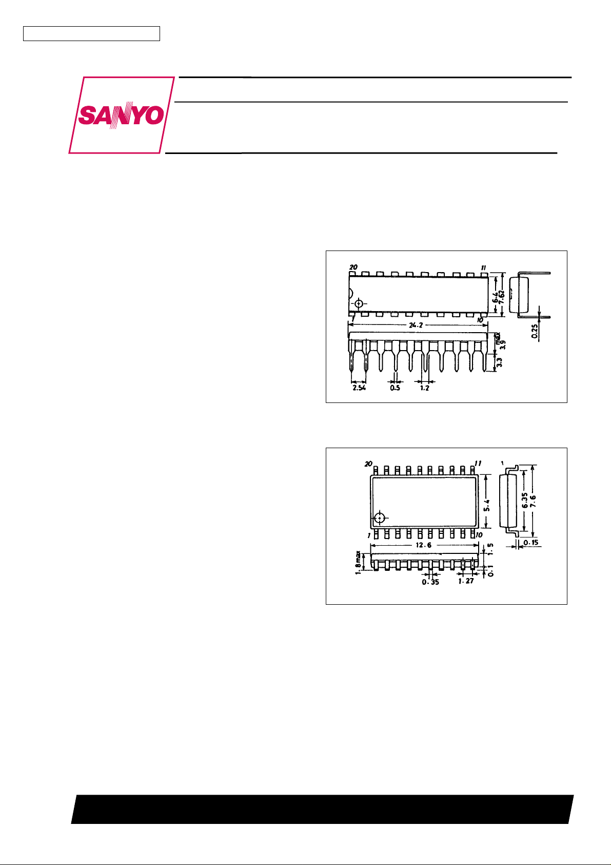
3021B-DIP20S
[LA1135]
SANYO : DIP20S
unit : mm
3036B-MFP20
[LA1135M]
SANYO: MFP20
SANYO Electric Co.,Ltd. Semiconductor Bussiness Headquarters
TOKYO OFFICE Tokyo Bldg., 1-10, 1 Chome, Ueno, Taito-ku, TOKYO, 110 JAPAN
93097HA(II)/D0994JN/O217KI/4034KI.TS(KOTO) No.1272-1/18
Page 2
LA1135, 1135M
Specifications
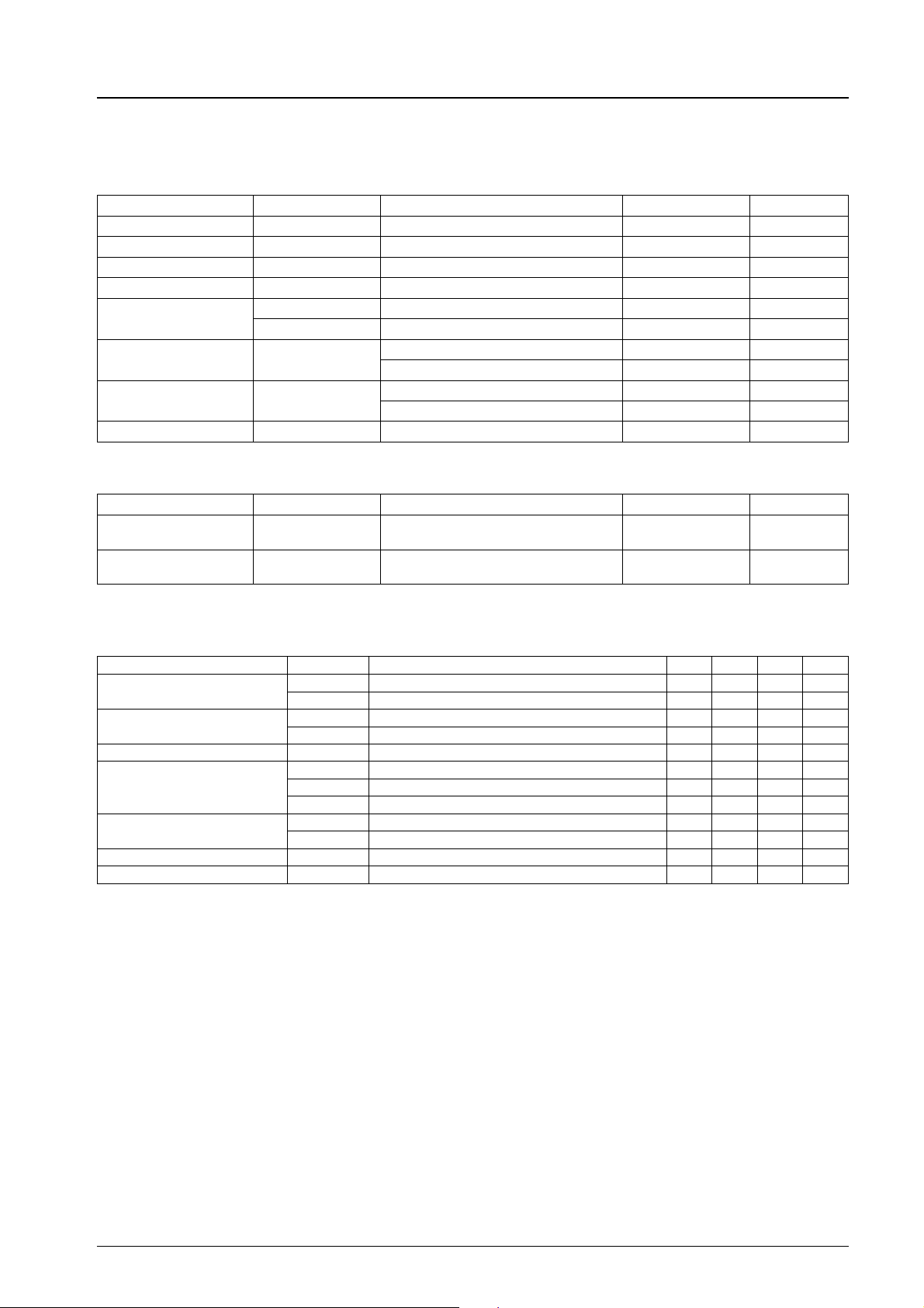
Maximum Ratings at Ta = 25°C
Parameter Symbol Conditions Ratings Unit
Maximum supply voltage V
Output voltage V
Input voltage V
Current drain I
Flow-out current I
Allowable power
dissipation
Operating temperature Topr LA1135 –20 to +70 °C
Storage temperature Tstg –40 to +125 °C
Operating Conditions at Ta = 25°C
Parameter Symbol Conditions Ratings Unit
Recommended supply
voltage
Operating supply voltage
range
max Pins 8, 14 16 V
CC
O
IN
CC
18
I
20
Pd max LA1135 730 mW
V
CC
V
op 7.5to12 V
CC
Pins 7, 10 24 V
Pin 6 5.6 V
Pins7+8+10+14 41 mA
Pin 18 2 mA
Pin 20 2 mA
LA1135M Ta % 60°C, with PCB 660 mW
LA1135M –40 to +80 °C
8V
Operating Characteristics at Ta = 25°C, VCC=8V,fr= 1 MHz, fm= 400 Hz, See specified Test
Circuit.
Parameter Symbol Conditions min typ max Unit
I
1 Quiescent 13.5 22.5 32.5 mA
Current drain
Detection output
Signal-to-noise ratio S/N 74 dBµ input, 30% mod 51.0 56.0 dB
Total harmonic distortion
Signal meter output
Input at signal meter output 1 V V
Local oscillation buffer output V
CC
I
2 130 dBµ input 20.0 30.0 41.0 mA
CC
V
1 16 dBµ input, 30% mod –29.0 –25.0 –21.0 dBm
O
V
2 74 dBµ input, 30% mod –15.0 –12.0 –9.0 dBm
O
THD1 74 dBµ input, 30% mod 0.3 1.0 %
THD2 74 dBµ input, 80% mod 0.3 1.0 %
THD3 130 dBµ input, 80% mod 0.4 2.0 %
V
1 Quiescent 0 0.3 V
SM
V
2 130 dBµ input 3.5 5.0 7.5 V
SM
1VSM= 1 V 18.0 24.0 30.0 dBµ
IN
BUF 320 380 mVrms
OSC
No. 1272-2/18
Page 3
LA1135, 1135M
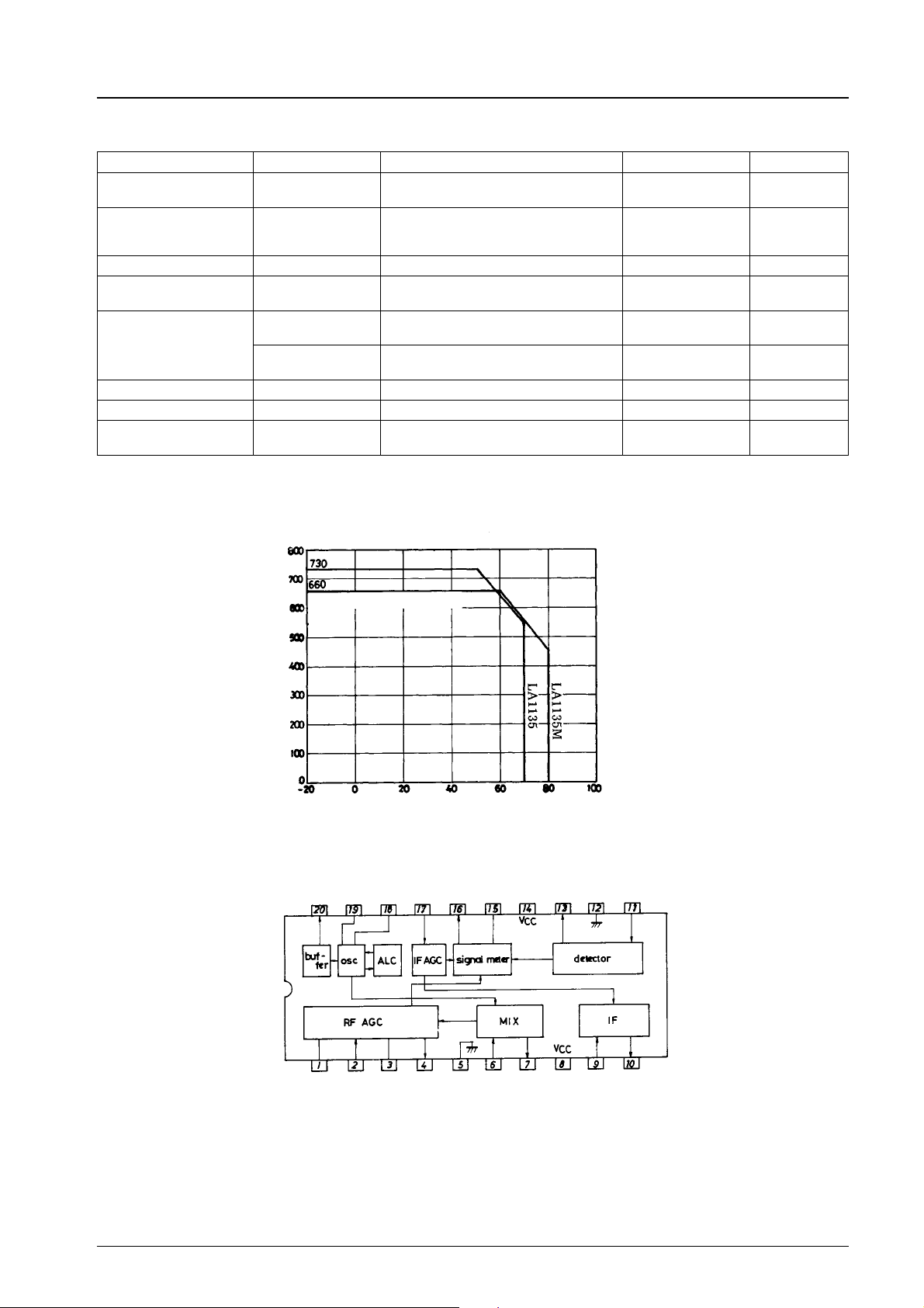
Reference Characteristics
Parameter Symbol Conditions typ Unit
Usable sensitivity Q.S. Input at S/N = 20 dB
Wide-band AGC
ON-state input
Detection output variation ∆V
Local oscillation variation
within broadcast band
Signal meter band * V
Selectivity 30 % mod ±10 kHz * 43 dB
IF interference IF. R. f
Image frequency
interference
O
∆V
OSC
SM-BW1
V
SM-BW2
IM. R. f
(2SK315 I
Reception 1.0 MHz quiescent
Interference 1.4 MHz non-mod
at input for AMT.D. ON
Input 74 dBµ → 130 dBµ 0.2 dB
V
L–V
OSC
74 dBµ input, frequency at
which output is reduced to 1/2
74 dBµ input, frequency at
which output is reduced to 1/10
= 600 kHz * 77.5 dB
r
= 1400 kHz * 52.0
r
=11mA)
DDS
H 15 mVrms
OSC
Note: *: Wide-band AGC OFF
( ): See circuit on page 7.
25.0 dBµ
82.0 dBµ
±1.5 kHz
–4.5/+7 kHz
(63.0)
dB
with 54 × 34 × 1.7 mm3PCB
Allowable power dissipation, Pd max – mW
Ambient temperature, Ta – °C
Equivalent Circuit Block Diagram
Pd max – Ta
No. 1272-3/18
Page 4
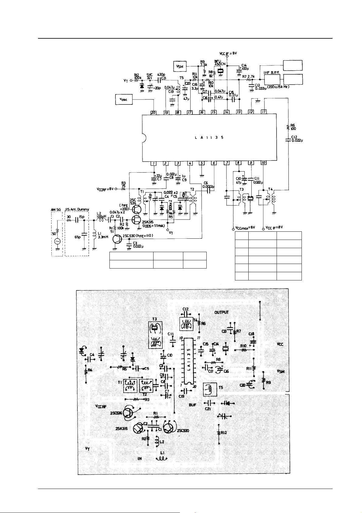
Test Circuit 1
VCC=8V,fr= 1 MHz, fm= 400 Hz
Unit (resistance: Ω, capacitance: F)
HF valve voltmeter
LA1135, 1135M
DC voltmeter
Distortion
meter
Valve
voltmeter
V
O
Varactor diode SVC321 (Sanyo)
Narrow-band filter BFU450CN (Murata)
Sample Printed Circuit Pattern
Coil
T1 YT-30020 (Mitsumi)
T2 YT-30018 (Mitsumi)
T3 CFMA-027 (Toko)
T4 YT-30007 (Mitsumi)
T5 YT-30008 (Mitsumi)
Cu-foiled area 105 × 120 mm
2
No. 1272-4/18
Page 5
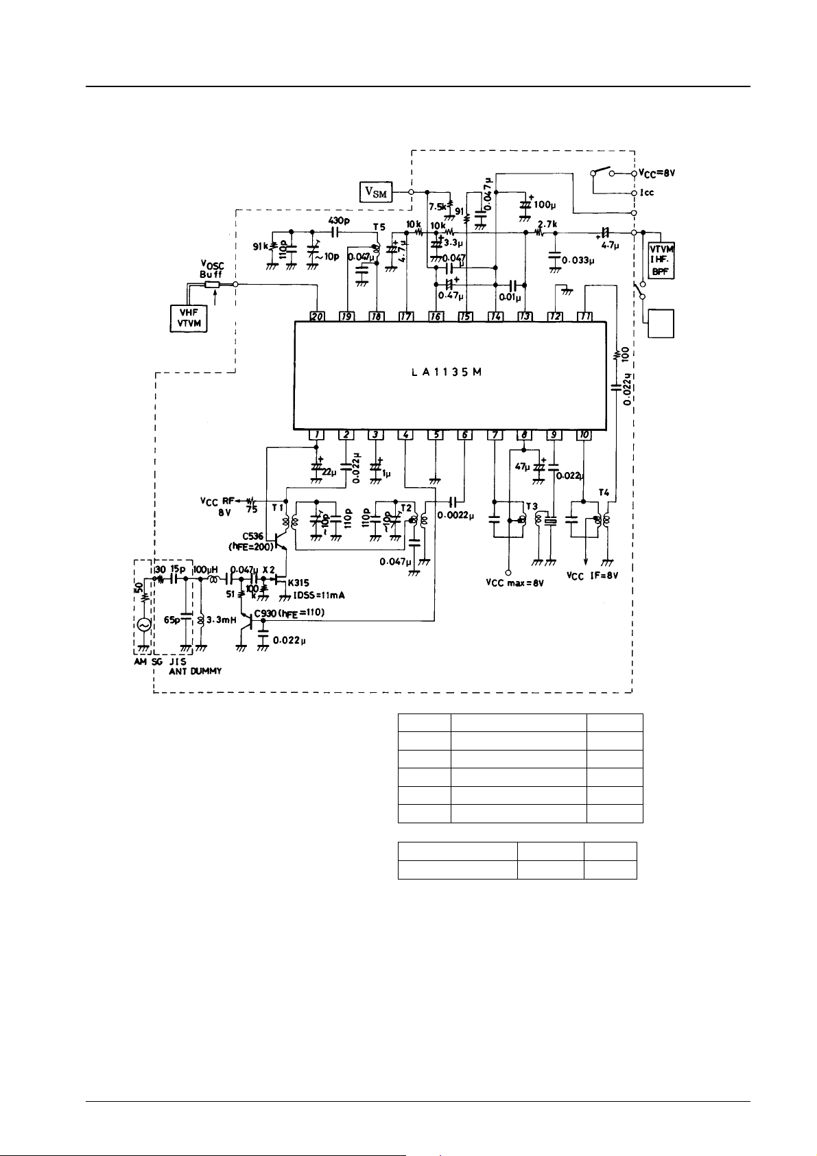
Test Circuit 2
VCC=8V,fr= 1 MHz, fm= 400 Hz
LA1135, 1135M
DC voltmeter
Detection output
Probe load open
Distortion meter
Unit (resistance: Ω, capacitance: F)
Coil
T1 YT-30202 (Mitsumi)
T2 YT-30018 (Mitsumi)
T3 CFMA-021A (Toko)
T4 YT-30007 (Mitsumi)
T5 YT-30008 (Mitsumi)
Varactor diode SVC321 (Sanyo)
Narrow-band filter BFU450CN (Murata)
No. 1272-5/18
Page 6
Proper cares in using IC
LA1135, 1135M
1. Bias condition: RF VCC% IF V
CC
2. Avoid coupling between the antenna tuning circuit and the local oscillation.
3. Connect detection capacitor C15 across pins 13 (output) and 14 (V
) so that no leakage of the IF signal to the GND line
CC
occurs. (If connected to GND, the tweet and the usable sensitivity may get worse.) Radiation from C15 may cause harmonics
in the IF signal to return to the RF stage, thereby leading to more tweet interference. So, connect C15 as close to pins 13, 14
as possible. Consider the direction of the capacitor and separate it from the ANT circuit.
4. For R9, use a semifixed resistor with V
considered.
SM
5. When designing the coils, consider the following conditions.
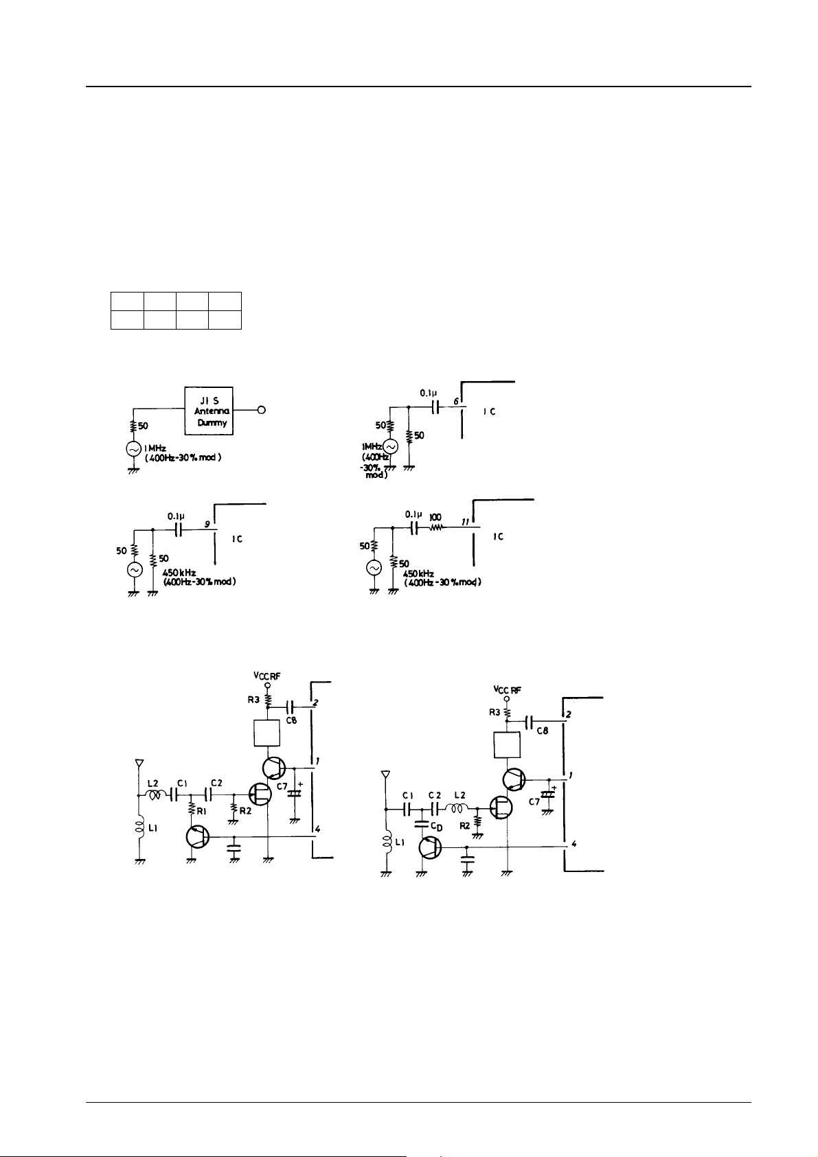
Shown below is the input level at each pin at which the detection output at f
ANT MIX IF Det
16.0 28.0 45.0 61.0
(dBµ)
= 400 Hz 30% mod becomes –25 dB.
m
How to apply input to each stage
ANT stage
MIX stage
ANT input
IF stage
Det stage
Unit (resistance: Ω, capacitance: F)
6. ANT damping
To make the ANT damping constant within the receiving band, change the application circuit as shown below.
Old circuit New circuit
Double tuning
Double tuning
Measures
Replace R1 with C
C
(2000 pF to 3000 pF or thereabouts)
D
.
D
Relocate L2.
Damping (600 kHz to 1400 kHz) Old circuit –15 dB
New circuit –4 dB
No. 1272-6/18
Page 7
LA1135, 1135M
7. Meaning of L2
If the RF stage is double-tunned, the difference in sensitivity within the RF band almost disappears, but an antireasonance
point of approximately 20 MHz appears, thereby leading to worse spurious characteristics. So, L2 is used to remove the SW
band.
8. Wide-band AGC
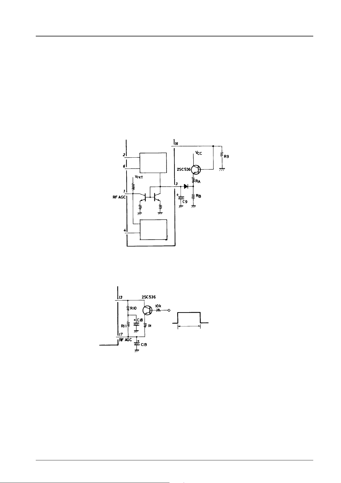
This IC contains 2-channel wide-band AGC. Pin 6 detects an undesired signal within the RF band and wide-band AGC is
applied. This detection sensitivity is determined inside the IC. Pin 2 detects an undesired signal outside the RF band. This
detection sensitivity is determined by R3. When 1 mVrms (f = 1 MHz) signal is applied to pin 2, AGC operates.
9. Measures against suppression of sensitivity
In the AGC circuit of the test circuit the presence of an undesired signal of high strength within the receiving band may cause
the desired signal to be suppressed when the desired signal is low or medium in strength. Shown below is the circuit
configuration where the necessary measures are taken against this suppression.
S meter output
Wide-band
AGC input
Wide-band
AGC
circuit
Circuit added
Sample constants
R
= 4.3 kΩ
A
R
= 3.0 kΩ
B
(V
-130 = 5.0 V)
SM
damping pin
ANT
ANT
damping
driver circuit
10. Transient response of S meter output at search, stop mode
The circuit configuration shown below is available to stabilize the transient response of the S meter output at the search, stop
mode.
Signal during searching from PLL
Unit (resistance: Ω)
11. When using LW (approximately 50°C or greater), additionally connect a resistor of 27 kΩ across pins 18 and 19 against
increase in local oscillation level. When using MW, no additional resistor is required.
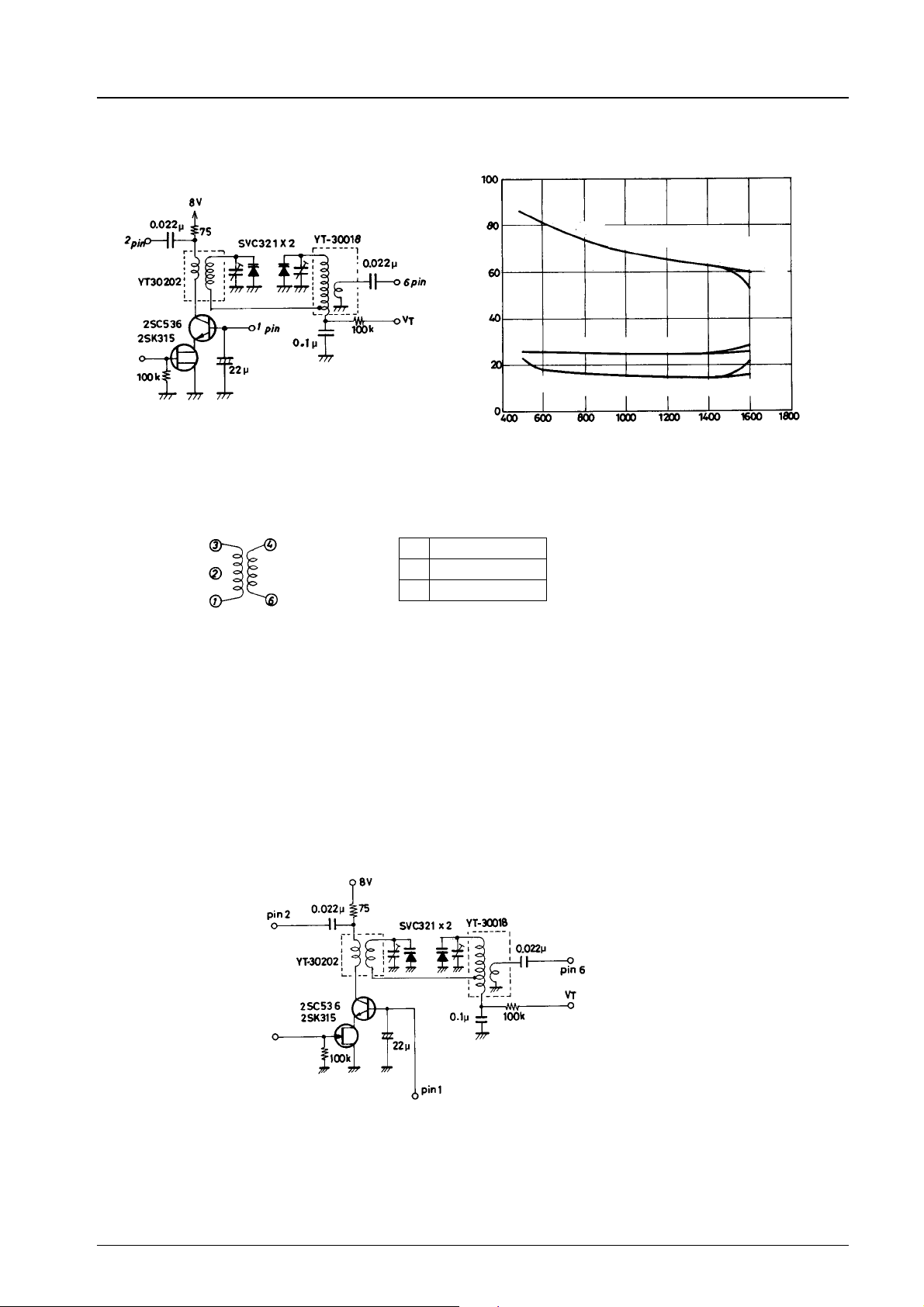
12. Improvement in image frequency interference
Change the RF double-tuning coil as follows, and the image frequency interference becomes 63 dB at f
= 1400 kHz.
r
(Q of the tuning circuit must not be decreased with resistor 100 kΩ.)
Continued on next page.
No. 1272-7/18
Page 8
Continued from preceding page.
LA1135, 1135M
Wide-band AGC OFF
Usable sensitivity S/N 20 dB
Maximum sensitivity at –25 dB output
Tracking at
each point
Image frequency interference – dB
Usable sensitivity, Maximum sensitivity – dBµ
Receiving frequency, fr– kHz
Unit (resistance: Ω, capacitance: F)
Specification for coil
YT-30202(Mitsumi)
1-3 84T
4-6 17T
2157-2239-649 (Sumida)
7BRS-9286A (Toko)
13. The variations (especially in case of small coupling coefficient) in the oscilation coil may cause a parasitic oscillation of
approximately 100 MHz to occur at the local oscillation buffer output (pin 20) at low temperatures. In this case, connect a
capacitor of 30 pF or greater across pin 20 and GND. (When the oscillation coil is used with no tap, no problem arises.)
14. The recommended double-tuning circuit has a loose coupling at 2T. Therefore, the change in the total number of turns may
affect the coupling coefficient subtly, causing a tight coupling and making the selectivity characteristic double-humped.
Especially for a receiving band of 1400 kHz or more, the tracking method may affect the band characteristic of sensitivity
and the cross modulation characteristic considerably. When making a design, check to see if critical coupling occurs or not.
15. Sensitivity difference at 600 kHz or less
In the application circuit configuration shown below, the bypass capacitor in the position where the tuning voltage is applied
and coupling L for double-tuning may cause an antiresonance point of 400 kHz to 600 kHz depending on the variations in
the coil, varactor diode, etc. The value of the bypass must be 0.047 µF or greater. The recommended value is 0.1 µF.
Unit (resistance: Ω, capacitance: F)
No. 1272-8/18
Page 9
LA1135, 1135M
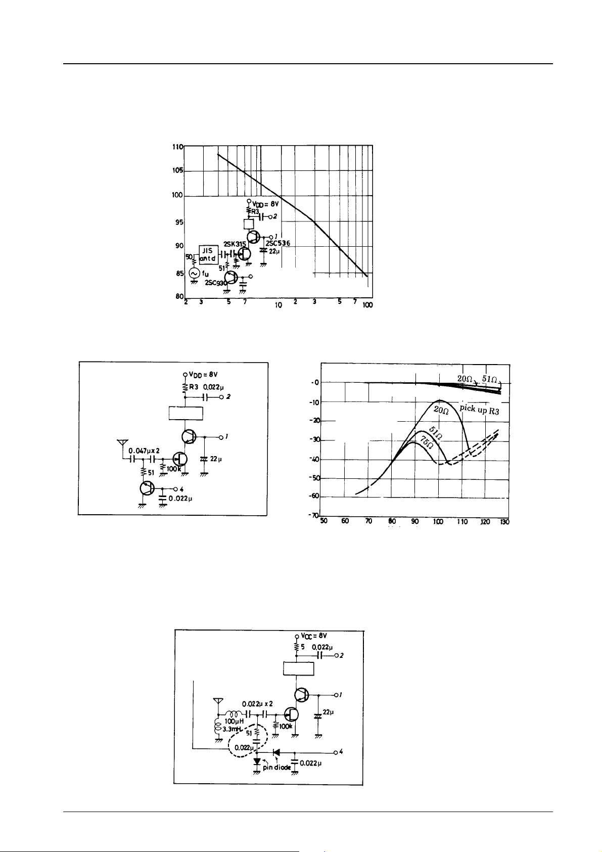
16. Measure against suppression of sensitivity in the presence of an undesired signal of high strength
(Sample application where two PIN diodes are used in the antenna damping circuit)
The LA1135 contains the wide-band AGC circuit (wide-band AGC with pin 2 input) against cross modulation which occurs
because an undesired signal of high strength distorts the FET input. The AGC = ON level depends on the value of external
resistor R3 as shown below.
Test conditions
Double-tuning
W.B.AGC-ON level – dBµ
ANT input level
at which ANTD is turned ON when
= 1.4 MHz is inputed at fr= 1 MHz
f
u
Resistor value, R – Ω
When a nonlinear element, such as transistor, is used for antenna damping, cross modulation which occurs when the transistor is
turned ON is as shown below.
Cross Modulation Characteristics
Cross modulation characteristic which is caused
by the ANT Tr when the
LA1135 wide-band
AGC-ON level (with
pin 2 input) is varied
Doubletuning
Desired:1.0 MHz 400 Hz 30% mod 74 dBµ
Undesired: 1.4 MHz non-mod
Wide-band AGC (pin 2 input)75Ω
Desired: 1.0 MHz 400 Hz
non-mod 74 dBµ
Undesired: 1.4 MHz 1 kHz
80% mod
Output – dB
Cross modulation which occurs when the
transistor for ANT damping is turned ON
Unit (resistence: Ω, capacitance: F)
Undesired input – dBµ
The dynamic range of the FET input covers up to approximately 110 dBµ of antenna input, but the AGC-ON level must be set
lower because of the bad effect shown above.
Therefore, there are some cases where it is difficult to receive a desired signal of low strength in the presence of an an undesired
signal of high strength. To solve this problem, a sample application circuit where two PIN diodes with good linearity are used for
antenna damping and its cross modulation characteristic are shown below.
Sample Application Circuit where two PIN diodes are used for ANT damping
Equivalent capacitance available
(Capacitance is desirable because
of a slight change in ANT damping
in the band)
(Approximately 3000 pF)
Doubletuning
Unit (resistance: Ω, capacitance: F)
No. 1272-9/18
Page 10
LA1135, 1135M
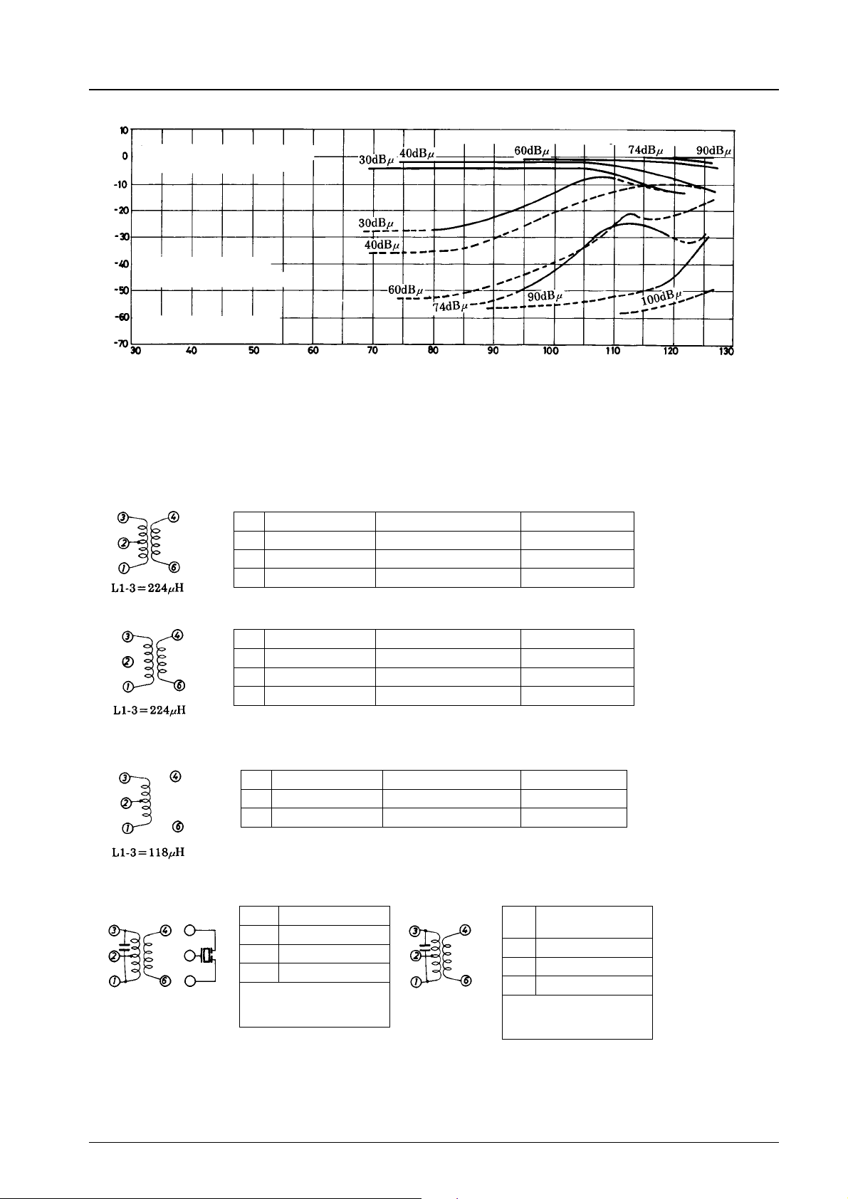
Cross Modulation Characteristics
Desired: 1.0 MHz fm= 400 Hz 30% mod
Undesired: 1.4 MHz non-mod
Desired: 1.0 MHz non-mod
Output – dB
Undesired: 1.4 MHz f
Pin 2 input W.B.AGC
External pickup R3 = 5 Ω
= 1 kHz 80% mod
m
Undesired input – dBµ
17. For details of the LA1135 wide-band AGC, refer to Technical Data No.79.
External Parts
(1) RF double-tuning coil
Primary
Application where two PIN diodes are used for ANT damping
Secondary
(2) OSC coil
(3) IFT (I)
YT-30020 (Mitsumi) 2157-2239-518A (Sumida) 7BRS-8934A (Toko)
1–2 2T 2T 2T
6–4 37T 40T 35T
2–3 82T 90T 75T
YT-30018 (Mitsumi) 2157-2239-517A (Sumida) 7BRS-8932A (Toko)
1–2 2T 2T 2T
6–4 15T 16T 14T
2–3 82T 90T 75T
YT-30008 (Mitsumi) 2157-2239-516 (Sumida) 7BR-5941Y (Toko)
1–2 29T 34T 29T
2–3 29T 35T 29T
High selectivity type
CFMA-027 (Toko)
1–2 69T
2–3 77T
4–6 14T
Center frequency 450 kHz
Qu=115±20%
Tuning capacitance 180 pF
YT-30042 (Mitsumi)
+SFP450H (Murata)
1–2 49T
4–6 27T
2–3 103T
Center frequency 450 kHz
Qu=45±20%
Tuning capacitance 180 pF
No. 1272-10/18
Page 11
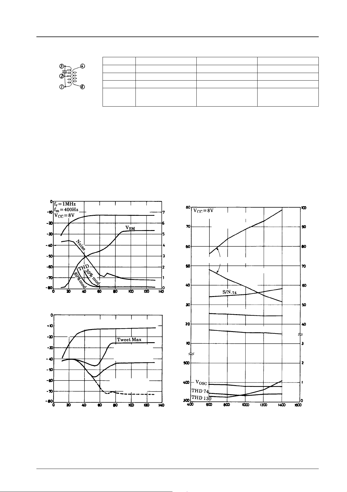
(4) IFT (II)
1–2 115T 111T 110T
4–6 6T 6T 6T
2–3 37T 36T 36T
(5) Varactor diode: SVC321
(6) FET at RF stage: 2SK315 F, G
2SK427 T, U
(7) Transistor for AGC
FET AGC: 2SC536 F, G
ANT damping: 2SC930 E
(8) Narrow-band resonator BFU450CN Murata
LA1135, 1135M
YT-30007 (Mitsumi) 4140-1289-164 (Sumida) 7MC-6272N (Toko)
Center frequency 455 kHz,
Qu = 110%
Tuning capacitance 180 pF
Center frequency 455 kHz
Qu = 110%
Tuning capacitance 180 pF
Center frequency 455 kHz,
Qu = 110%
Tuning capacitance 180 pF
Output – dBm
Signal characteristic
f
r
Overall Characteristics
Detection output at 30% mod
Input voltage – dBµ
Tweet Input Characteristics
= 900 kHz fm= 400 Hz 30% mod
Complete tuning
(Beat max. at
900 kHz tuning)
–V
SM
THD–% V
Tracking at each point
Wide-band AGC cutoff
M.S., Q.S. – dBµ
Band Characteristics
IF interference
Image frequency
interference
Input at 20 dB S/N
Input at –25 dBm output
–dB
–74
Output – dBµ
Complete tuning
(Zero beat)
ANT input – dBµ
Total harmonic distortion, THD – % IF interference, image frequency interference, S/N
Receiving frequency, fr– kHz
No. 1272-11/18
Page 12
LA1135, 1135M
– dBm
O-74
Detection output, V
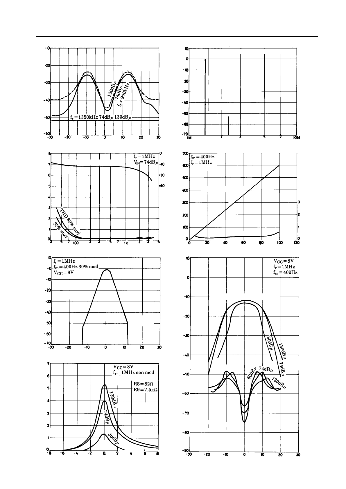
Detuning Characteristics
Vary VTso that
tweet output is
maximized at each
point.
Frequency deviation, ∆f– kHz
THD–f
Detection output 30% mod
m
Spurious Characteristics
Difference in input at –25 dBm output
Output – dBµ
Receiving frequency, fr–Hz
Detection Output, THD – Modulation Characteristics
Input: 74 dBµ
Output – dBµ
Detection output
Total harmonic distortion, THD – %
Selectivity – dB
–V
SM
fm–Hz
Selectivity Characteristics
W.B.AGC
Difference in
input at –25 dBm
output
operation
Frequency deviation, ∆f – kHz
Detuning Characteristics
Using narrow-band filter
Output – mVrms
Output – dBm
Distortion
Modulation – %
Detuning Characteristics
Detection output 30% mod
Noise
THD–%
S meter output, V
Frequency deviation, ∆f – kHz
Frequency deviation, ∆f – kHz
No. 1272-12/18
Page 13
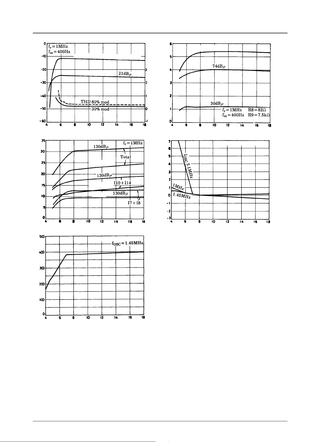
LA1135, 1135M
– dBm
O
Output, V
–mA
CC
,THD–V
V
O
CC
Detection output-Input: 74 dBµ
Detection output
Supply voltage, V
I
CC–VCC
CC
–V
Quiescent
Quiescent
Quiescent
VSM–V
CC
Input: 130 dBµ
–V
SM
S meter output, V
Total harmonic distortion, THD – %
Using narrow-band filter
Supply voltage, VCC–V
∆f–V
CC
OSC coil 1/2 tap
Current drain, I
–mV
OSC
V
Supply voltage, V
V
OSC–VCC
CC
–V
OSC coil 1/2 tap
Supply voltage, VCC–V
Frequency deviation, ∆f – kHz
Supply voltage, V
CC
–V
No. 1272-13/18
Page 14
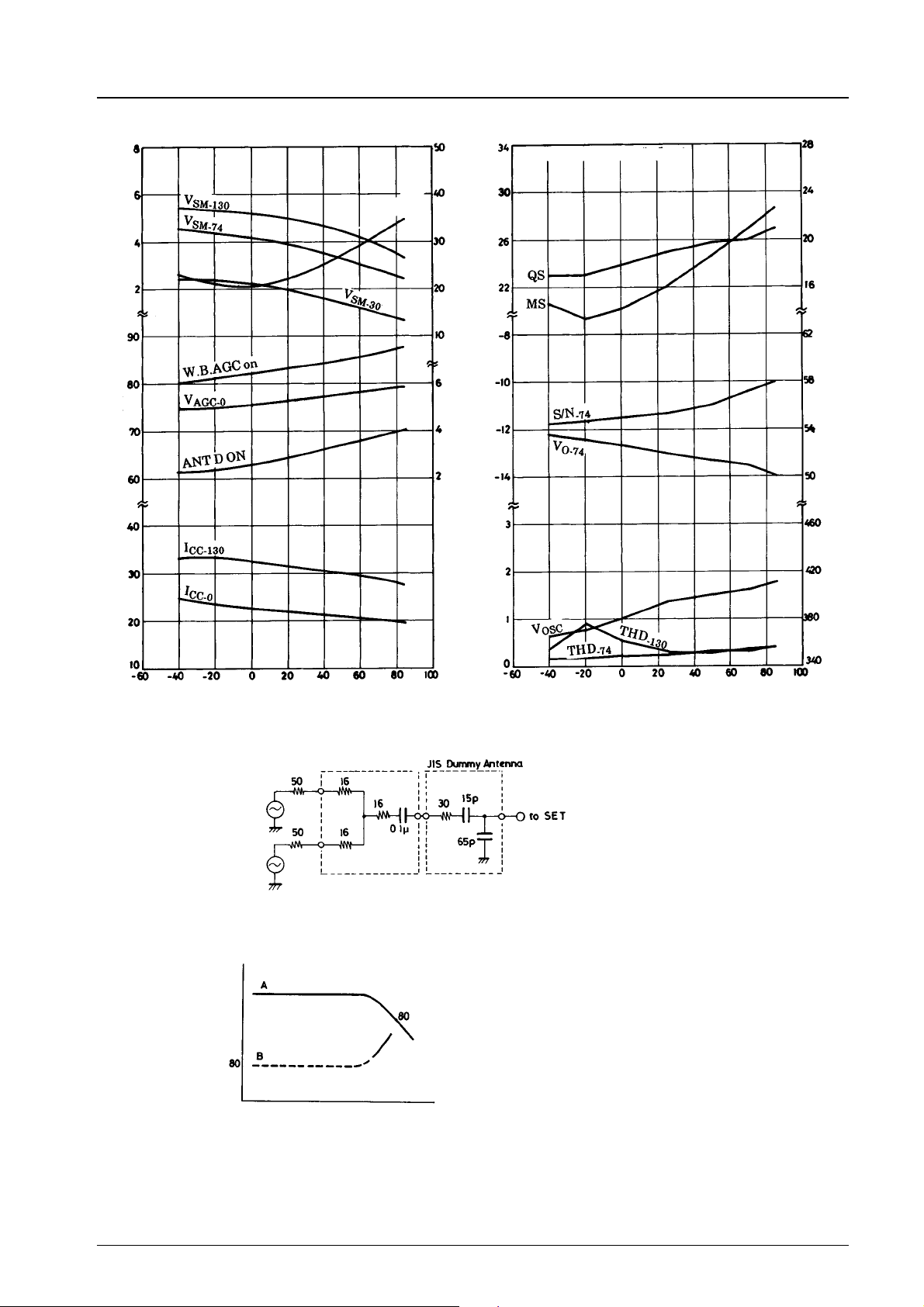
LA1135, 1135M
–V
SM-47
,V
SM-130
V
S meter output,
ANT D ON input – dBµ
W.B.AGC ON input – dBµ
–mA
CC
Temperature Characteristics
VSM=1V
input
= 1V input – dBµ
SM
V
–V
AGC-0
V
Temperature Characteristics
Usable sensitivity (Input at 20 dB S/N)
– dBm
O-74
V
Maximum sensitivity, MS – dBµ
–dBV
–74
S/N
– mVrms
Current drain, I
Ambient temperature, Ta – °C
Total harmonic distortion, THD – % Usable sensitivity, Q.S. – dBµ
Cross Modulation Characteristics Testing Method
2-signal pad JIS Dummy ANT
Desired signal ANT input
Output
Desired signal ANT input
Solid line —— Interference
Dotted line ---- No interference
OSC
Ambient temperature, Ta – °C
Unit (resistance:Ω, capacitance: F)
A: Desired signal 80 dBµ 400 Hz 30% mod.
The strength of an undesired signal
(non-mod) causes the desired signal to
be suppressed.
B: Desired signal 80 dBµ non-mod.
The strength of an undesired signal (400
Hz 80% mod) causes interference to
occur.
No. 1272-14/18
Page 15
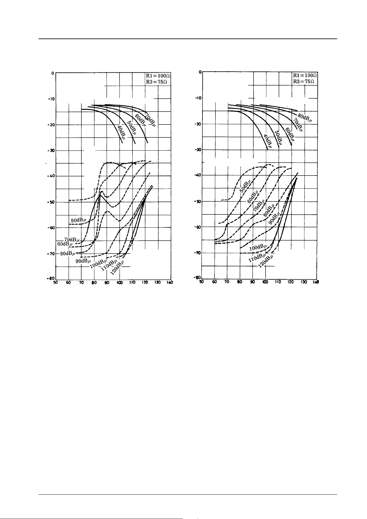
LA1135, 1135M
Desired 1.0 MHz
Undesired 1.4 MHz
Output – dBµ
Cross Modulation Characteristics
400 Hz
30% mod
non mod
Desired input 80 dBµ
dBµ
Desired input 40
Desired 1.4 MHz
Undesired 1.44 MHz
Desired input 40 dBµ
Output – dBµ
Cross Modulation Characteristics
400 Hz
30% mod
non mod
Desired input 90 dBµ
Desired 1.0 MHz
Undesired
Undesired input – dBµ
non mod
1.4 MHz
400 Hz
80% mod
Desired 1.4 MHz
Undesired
Undesired input – dBµ
non mod
1.44 MHz
400 Hz
80% mod
No. 1272-15/18
Page 16
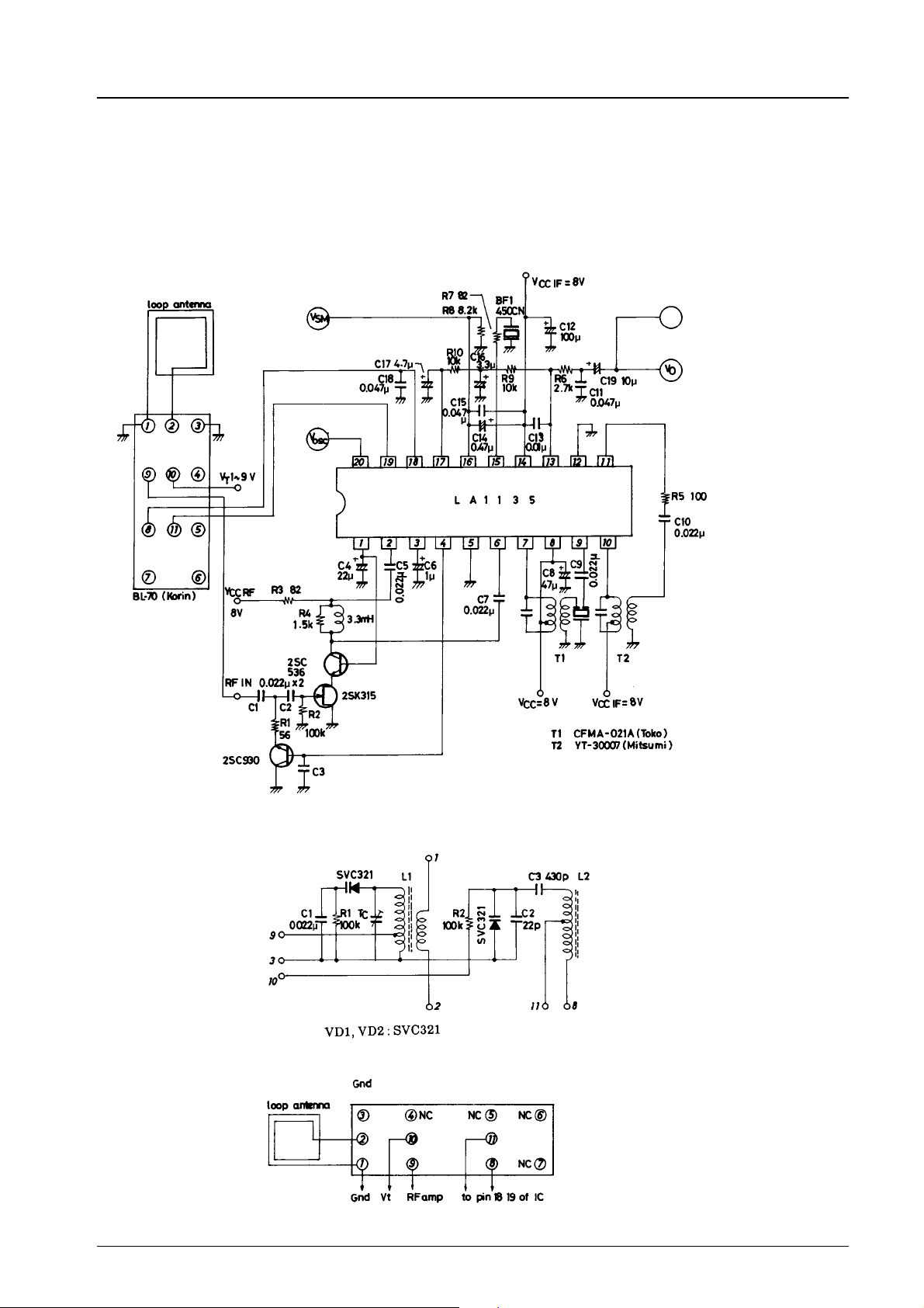
LA1135, 1135M
Specification for LA1135 loop ANT
(1) Features of specification for LA1135 loop ANT
1) Excellent high-input characteristic
The antena damping circuit prevents the antena circuit from being magnetic-saturated, which results in worsened
characteristic, at a high input.
2) Excellent cross modulation characteristic
(2) Application circuit
DC voltmeter
HF valve voltmeter
Distortion meter
Valve voltmeter
(3) Circuit configuration and connection
3-1 Circuit configuration
3-2 Connection (bottom view)
Unit (resistance: Ω, capacitance: F)
Unit (resistance: Ω, capacitance: F)
No. 1272-16/18
Page 17
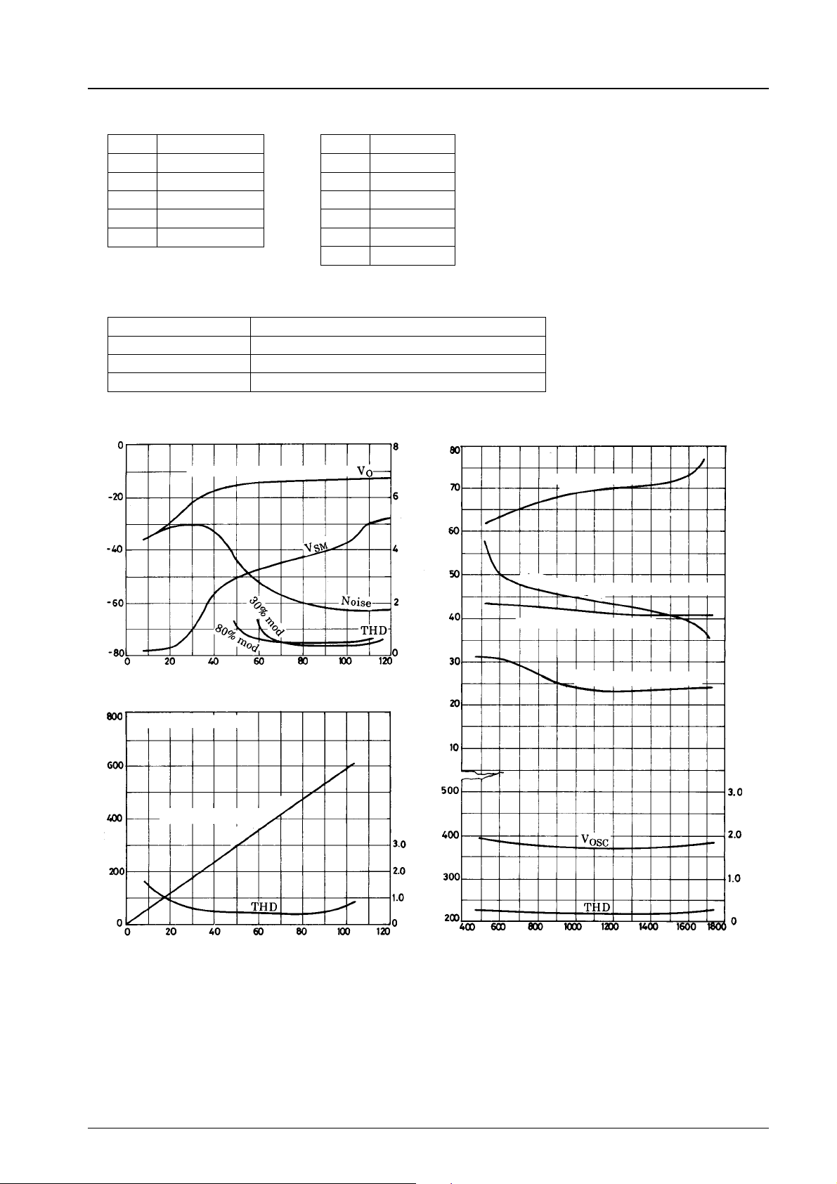
3-3 Pin name
LA1135, 1135M
Pin No. Pin Name
1 Loop ANT
2 Loop ANT
3 RF AMP GND side
4NC
5NC
Pin No. Pin Name
6NC
7NC
8 Local OSC
9 RF output
10 Tuning voltage
11 Local OSC
(4) Specification
Receiving frequency band MW BAND
Tuning voltage 1 to 9 V
Loop ANT 42579719100 (LA-1500), 4257976000 (LA-100A) (Korin)
IC LA1135
Overall Characteristics
Detection output at 30% mod
–V
SM
V
Output – dBµ
THD–%
Output – dBµ
Band Characteristics
IF interference
Image frequency interference
S/N 20 dB sensitivity
Input voltage – dBµ
Detection Output, THD – Modulation Degree
Input 74 dBµ
Detection output V
O
Output – mV
Modulation degree – %
–mW
OSC
V
THD–%
Input at V
= –25 dBm
O
Receiving frequency – kHz
THD–%
No. 1272-17/18
Page 18
LA1135, 1135M
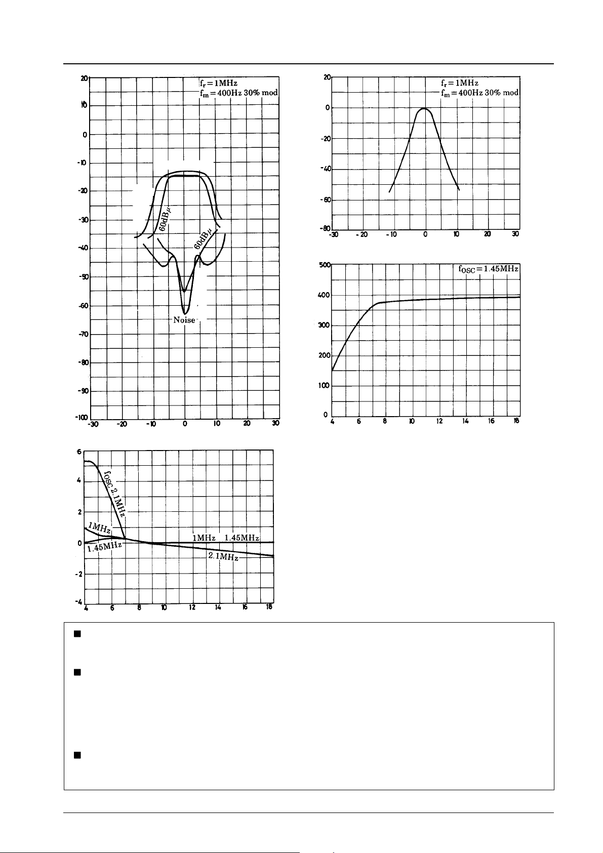
Output – dBµ
Detuning Characteristics
Detection output
Input 74 dBµ
Input 74 dBµ
Selectivity – dB
–mW
OSC
V
Selectivity Characteristics
Frequency deviation – kHz
V
OSC–VCC
Frequency deviation – kHz
∆f–V
CC
Supply voltage, VCC–V
Frequency deviation, ∆f – kHz
Supply voltage, VCC–V
No products described or contained herein are intended for use in surgical implants, life-support systems,
aerospace equipment, nuclear power control systems, vehicles, disaster/crime-prevention equipment and the like,
the failure of which may directly or indirectly cause injury, death or property loss.
Anyone purchasing any products described or contained herein for an above-mentioned use shall:
1 Accept full responsibility and indemnify and defendSANYOELECTRICCO.,LTD.,itsaffiliates, subsidiaries and
distributors and all their officers and employees, jointly and severally, against any and all claims and litigation
and all damages, cost and expenses associated with such use:
2 Not impose any responsibility for any fault or negligence which may be cited in any such claim or litigation on
SANYO ELECTRIC CO., LTD.,its affiliates, subsidiaries and distributors or any of their officers and employees
jointly or severally.
Information (including circuit diagrams and circuit parameters) herein is for example only; it is not guaranteed for
volume production. SANYO believes information herein is accurate and reliable, but no guarantees are made or
implied regarding its use or any infringements of intellectual property rights or other rights of third parties.
This catalog provides information as of September,1997.Specificationsandinformationhereinaresubjecttochangewithoutnotice.
No. 1272-18/18
 Loading...