

Page 1
LA1265
Ordering number : EN1820C
FM/AM Tuner of Electronic Tuning Type
Monolithic Linear IC
SANYO Electric Co.,Ltd. Semiconductor Bussiness Headquarters
TOKYO OFFICE Tokyo Bldg., 1-10, 1 Chome, Ueno, Taito-ku, TOKYO, 110 JAPAN
N2897HA (KT)/40194HK/O077KI/D095KI/2255KI, TS No.1820-1/15
Functions
FM : IF amplifier, quadrature detector, AF preamplifier,
signal meter, tuning indicator drive output (common
with stop signal, muting drive output).
AM : RF amplifier, MIX, OSC (with ALC), IF amplifier,
detector, AGC, signal meter, tuning indicator drive
output (common with stop signal).
Features
• Minimum number of external parts required.
• Excellent S/N.
• Local OSC with ALC.
• Local OSC buffer.
• Tuning indicator pin (common with narrow-band stop
signal and muting drive output).
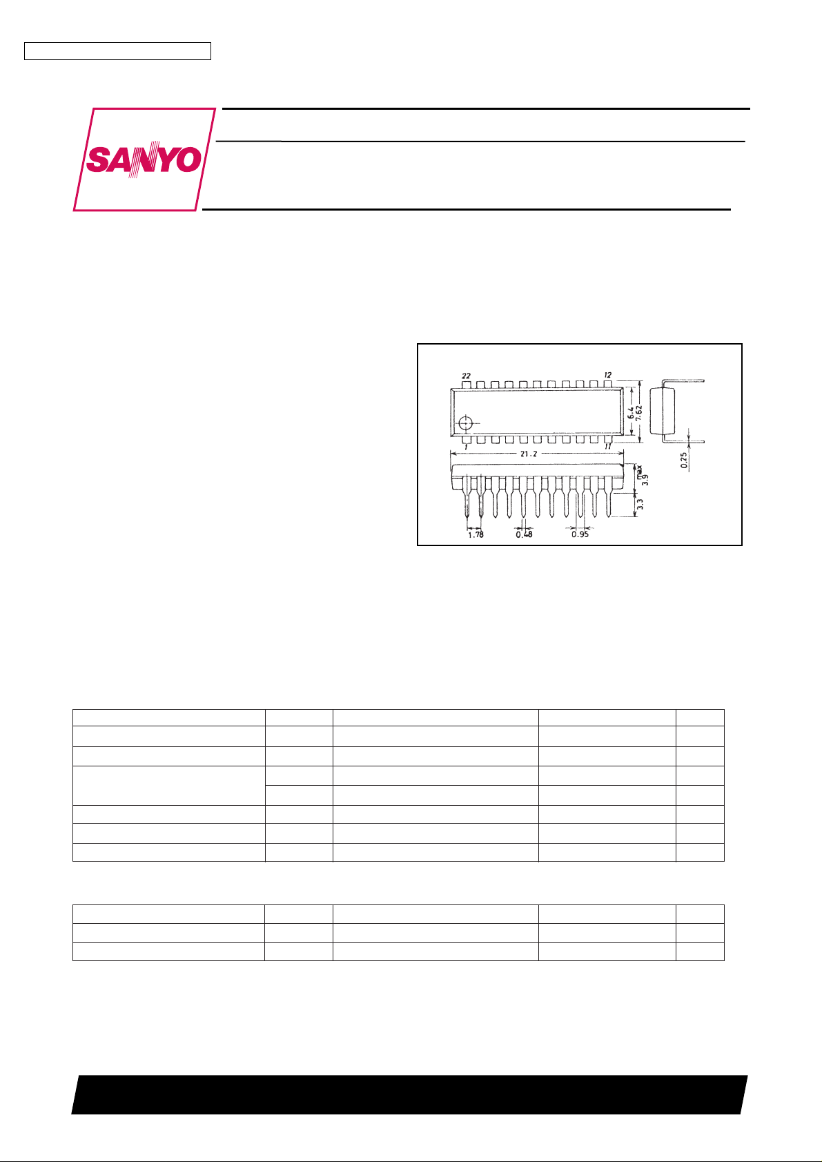
Package Dimensions
unit : mm
3059-DIP22S
[LA1265]
SANYO : DIP22S
• Variable stop sensitivity (variable separately for FM, AM)
• Low whistle.
• Signal meter pin.
Specifications
Maximum Ratings
at Ta=25°C, See specified Test Circuit.
Parameter Symbol Conditions Ratings Unit
Maximum supply voltage V
CC
max Pins 7, 8, 17 16 V
Flow-in current I
8
Pin 8 20 mA
Flow-out current I
20
Pin 20 1 mA
I
22
Pin 22 2 mA
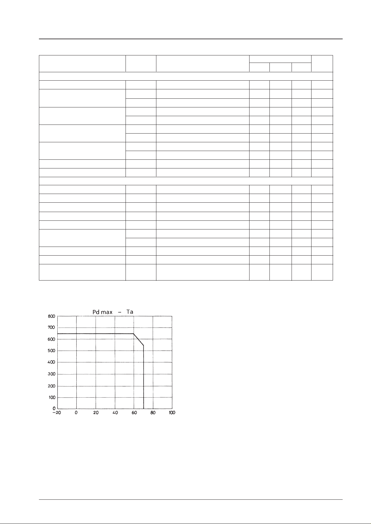
Allowable power dissipation Pd max Ta≤60°C 650 mW
Operating temperature Topr –20 to +70 °C
Storage temperature Tstg –40 to +125 °C
Operating Conditions at Ta=25°C
Parameter Symbol Conditions Ratings Unit
Recommended operating voltage V
CC
8.5 V
Operating voltage range V
CC
op 6 to 14 V
Page 2
Operating Characteristics at Ta=25°C, V
CC
=8.5V, See specified Test Circuit
Parameter Symbol Conditions
Ratings
min typ max
Unit
[AM : f=1MHz]
Quiescent current Icco No input 18 26 mA
Detection output VO1 VIN=20dBµ, 400Hz, 30% mod. 30 50 90 mV
VO2 VIN=80dBµ, 400Hz, 30% mod. 110 160 220 mV
S/N S/N1 VIN=20dBµ 16 20 dB
S/N2 VIN=80dBµ 49 54 dB
Total harmonic distortion THD1 VIN=80dBµ, 400Hz, 30% mod. 0.3 1.0 %
THD2 VIN=107dBµ, 400Hz, 30% mod. 0.5 2.0 %
Signal meter output VSM1 No input 0 0 0.2 V
VSM2 VIN=80dBµ 2.4 2.8 3.1 V
LED lighting sensitivity VLED on I
LED
=1mA 15 24 33 dBµ
Local OSC buffer output V
OSC
f
OSC
=1.45MHz 220 275 330 mV
[FM : f=10.7MHz]
Quiescent current Icco No input 20 28 mA
Input limiting sensitivity –3dBL.S. 3dB down, 400Hz, 100% mod. 31 37 dBµ
Demodulation output V
O
VIN=10dBµ, 400Hz, 100% mod. 240 330 460 mV
S/N S/N VIN=100dBµ 78 84 dB
Total harmonic distortion THD VIN=100%dBµ, 400Hz, 100% mod. 0.03 0.3 %
Signal meter output VSM1 No input 0 0 0.2 V
VSM2 VIN=100dBµ 1.5 2.7 3.1 V
LED lighting sensitivity LED-on I
LED
=1mA 35 50 65 dBµ
LED lighting bandwidth LED-BW VIN=100dB, I
LED
=1mA 90 120 160 kHz
AM rejection ratio AMR V
IN
=100dBµ, FM=400Hz 45 60 dB
100% mod. AM=1kHz 30% mod.
LA1265
No.1820-2/15
Ambient temperature, Ta – °C
Allowable power dissipation, Pd max – mW
Page 3
LA1265
No.1820-3/15
How to use the LA1265
1. LED lighting, muting drive output, stop signal (SD).
• For LED lighting, muting drive output, stop signal, the output at
pin 8 is used.
• The voltage on pin 8, when tuned, turns from "H" to "L".
(Active-Low)
• Signal bandwidth at pin 8.
– For AM, the bandwidth depends on the CF (BFU450CN) at
pin 11. If a capacitor is connected in place of the CF, the
bandwidth will get wider.
– For FM, the bandwidth depends on the resistance across pins
9 and 20. If the resistance is increased, the bandwidth will get
narrower. R=15kΩ makes the bandwidth approximately
120kHz.
• Sensitivity adjustment of LED, muting, stop signal.
– For FM, the semifixed variable resistor across pin 13 and GND is used.
– For AM, the semifixed variable resistor across pins 13 and 14 is used. Be sure to start adjustment for FM, and then
make adjustment for AM. For the stop signal sensitivity and FM stop signal bandwidth, the variations should be
considered and it is recommended to use the semifixed variable resistor for adjustment.
• LED lighting sensitivity setting for AM.
For the LED lighting sensitivity setting for AM, it is desirable that the IC input be 30dBµ (antenna input :
approximately 50dB/m). In this case, the value of VR1 is 30kΩ.
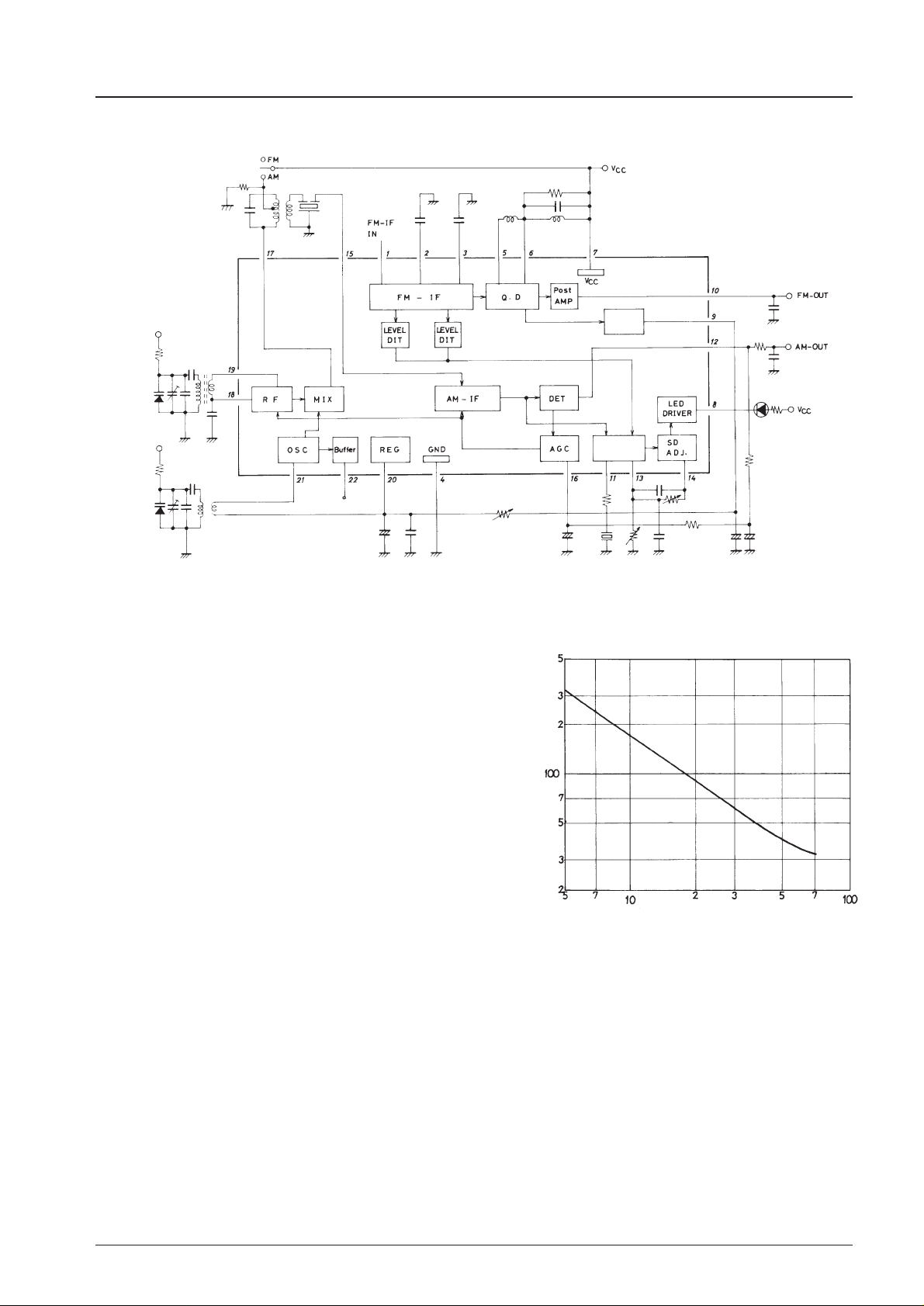
Equivalent Circuit Block Diagram
Resistance across pins 9 and 20 – kΩ
LED Lighting Bandwidth – Resistance across pins 9 and 20
LED lighting bandwidth – kHz
S Carve
S meter
Page 4
LA1265
No.1820-4/15
3. Local OSC buffer output
• When local OSC buffer output wave form is saw-toothed at the SW mode, connect a resistance of 1.2kΩ or
thereabouts across pin 22 and GND.
4. AM input pin
• It is desirable that the AM input pin (pin 19) be L-coupled to pin 18.
• Inputting to pin 19 can be done by DC-cutting with a capacitor. However, an unbalance in the RF amplifier
(differential amplifier) causes gain drop and whistle worsening.
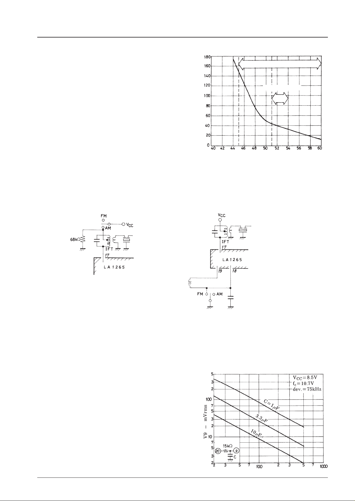
5. Capacitance across pin 9 and GND.
A large capacitance across pin 9 and GND may cause a misstop
at an adjacent channel when the channel select speed is made
faster at the automatic channel select mode. In this case, decrease
the capacitance across pin 9 and GND. However, if too
decreased, the LED will flutter at low modulation frequencies at
the time of detuning. Therefore, it is recommended to fix the
capacitance across pin 9 and GND to be 3.3µF to 10µF. The
relation between modulation frequency and demodulation output
voltage on pin 9 with the capacitance across pin 9 and GND as a
parameter is shown right.
• LED lighting sensitivity setting for FM.
– For the LED lighting sensitivity setting for FM, the IC
input may be 45dBµ to 60dBµ. With the variations in the
front end considered, it is ideal that the IC input in a
standard receiving set be 51dBµ to 54dBµ. The lower
value of VR2 for the LED lighting sensitivity setting is as
illustrated right. Since the variations in the front end cause
the IC input setting sensitivity to vary, it is recommended
to use a value of VR2 at an input voltage lower than a
standard setting by 6dB or greater. For example, if IC
input 53dBµ is taken as a standard, use VR2≤100kΩ at IC
input 47dBµ.
2. AM/FM changeover
• Two selections are available for changeover as shown below
: (A) pin 17-used method and (B) pin 18-used method.
• For (A), the voltage on pin 17 relative to VCC(pin 7) must be within the range of –0.8V to +0.1V. If not within this
range, distortion and selectivity will get worse.
• For (A), a resistance of 68kΩ at the IFT cold terminal, which is used to prevent the changeover circuit from
malfunctioning, must be connected.
(A) pin 17-use method for AM/FM changeover (B) Pin 18-used method for AM/FM changeover
IC input – dBµ
Semifixed Variable Resistor for FM
VR2 semifixed variable resistor value – kΩ
LED lighting sensitivity setting for FM
Ideal setting range
Modulation frequency – Hz
V9 – Modulation Frequency
Page 5
LA1265
No.1820-5/15
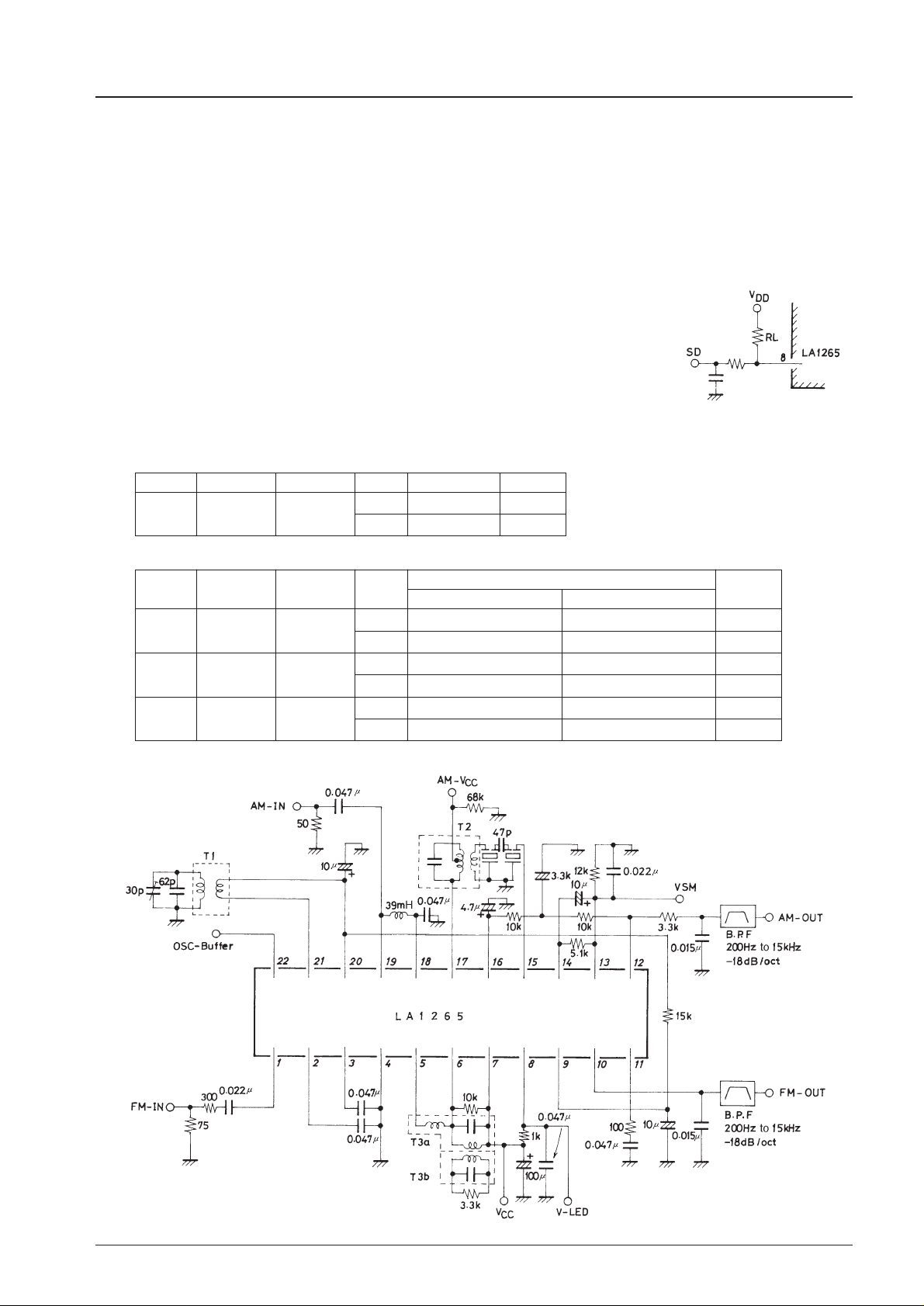
– Parameter Frequency – Admittance Unit
IF γi1 10.7MHz
r
i
330 Ω
c
i
20 pF
FM
– Parameter Frequency –
RF γi19 1MHz
r
i
r
o
c
i
Admittance
Unit
kΩ
pF
AGC-off (V16=1.4V) AGC-on (V16=2.5V)
15 16
4 4
MIX γo17 500kHz
c
o
kΩ
pF
– –
3 3
r
i
IF γi15 500kHz
c
o
kΩ
pF
2 2
10 8
AM
6. If the coupling coefficient of the local OSC coil is small and an antiresonance point of approximately 100MHz is
present or the stray capacitance across pins 22 and 21 is large, a parasitic oscillation of approximately 100MHz may
occur in the buffer output (pin 22). In this case, connect a capacitance of approximately 30pF across pin 22 and GND.
7. AM OSC coil
Generally speaking, the following should be noted. Avoid winding with loose coupling between primary side and
secondary side (especially SW1, SW2). To put it concretely, the pot core type is better than the screw core type which
is loose in coupling. This prevents the local OSC frequency from turning third resonance frequency related to the
coupling coefficient.
8. Resistance across pin 8 and VDD.
If pin 8 is used for the stop signal (SD) only, without using LED, it is recommended to fix
resistance RLacross pin 8 and GND to be 51kΩ to 100kΩ.
9. To prevent whistle from worsening, make the pattern of AM output pin 12 as short as
possible.
Input/Output Admittance
Test Circuit : FM, AM-MW
T1 4147-1457-177 (Sumida)
T2 HW-40174 (Mitsumi)
T3a HW-40130, T3b HW-40131 (Mitsumi)
Unit (resistance : Ω, capacitance : F)
Page 6
LA1265
No.1820-6/15
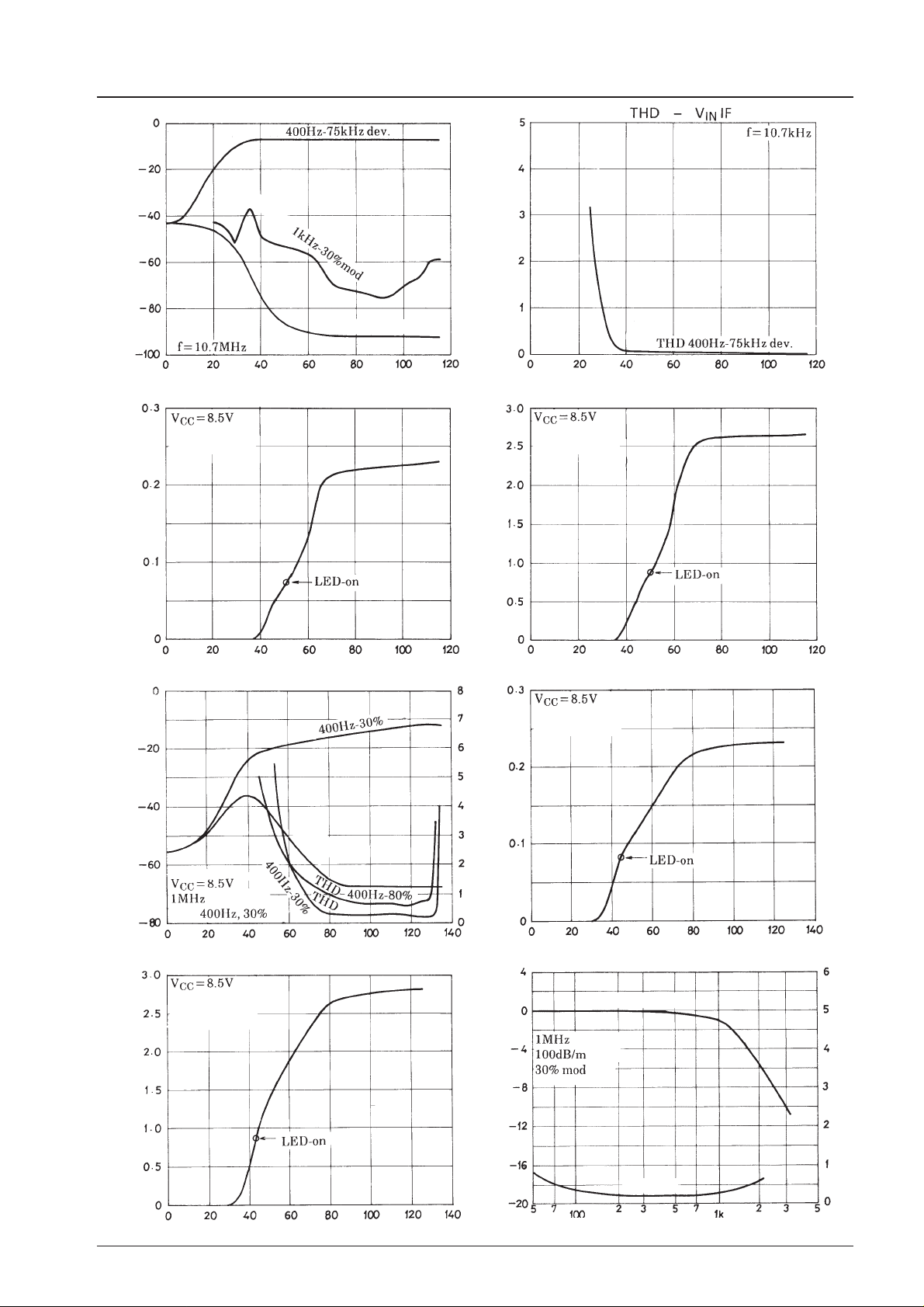
IF input voltage – dBµ
FM Input/Output Characteristics
Detection output, Noise voltage – dBm
Noise voltage
IF input voltage – dBµ
FM Signal Meter Current Characteristic
Signal meter current, I
SM
– mA
Non-modulation
See test circuit.
Antenna input voltage – dBm
MW Input/Output Characteristics
Noise voltage, Detection output – dBm
Total harmonic distortion, THD – %
reception
Antenna input voltage – dBm
AM Signal Meter Voltage Characteristic
Signal meter voltage, V
SM
– V
Antenna input voltage – dBm
AM Signal Meter Current Characteristic
Signal meter current, I
SM
– mA
Non-modulation
See test circuit.
Non-modulation
See test circuit.
Modulation frequency – Hz
MW Fidelity Characteristics
Attenuation – dB
Total harmonic distortion, THD – %
reception
Attenuation
Distortion
input
Noise
voltage
Mod.
IF input voltage – dBµ
FM Signal Meter Voltage Characteristic
Signal meter voltage, V
SM
– V
Non-modulation
See test circuit.
IF input voltage – dBµ
Total harmonic distortion, THD – %
AM output
Page 7
LA1265
No.1820-7/15
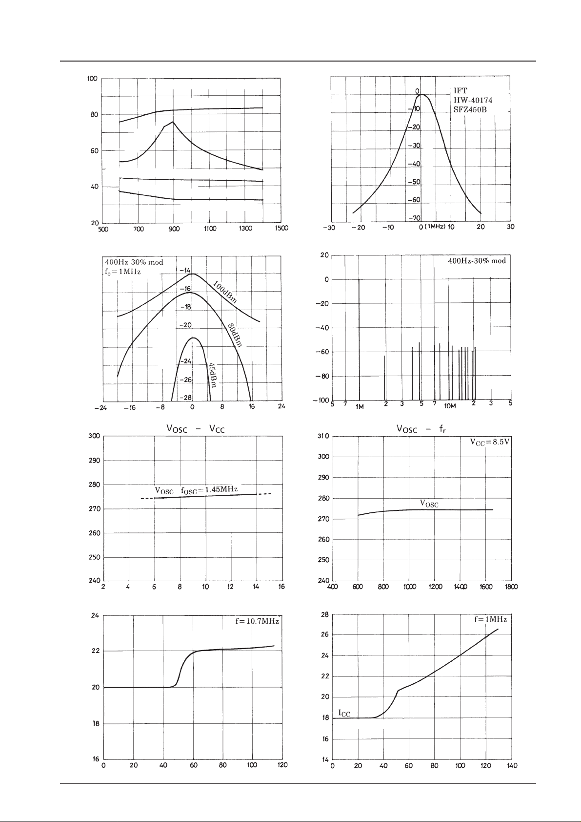
Receiving frequency, fr– kHz
MW Reception Characteristic
Sensitivity – dB/m Interference – dB
Tracking adjust at each frequency
IF interference
Frequency deviation, ∆f – Hz
MW Detuning Characteristic
Detection
output – dBm
Supply voltage, VCC– V
Local OSC buffer output, V
OSC
– mV
Local OSC buffer output, V
OSC
– mV
IF input voltage – dBµ
Current drain, I
CC
– mA
Receiving frequency, fr– kHz
Frequency deviation, ∆f – kHz
Selectivity Characteristic
Attenuation – dB
Output 25mV const.
Frequency, f – Hz
Spurious Characteristic
Response – dB
Reception : 1kHz
(400Hz-30% mod.,
detection output 20mV)
Max. sensitivity
Usable sensitivity (400Hz-30% mod., S/N=20dB)
Image
interference
FM Current Drain Characteristic
Antenna input voltage – dBm
Current drain, I
CC
– mA
AM Current Drain Characteristic
I
CC
(including
no LED current)
(including no LED current)
Page 8
LA1265
No.1820-8/15
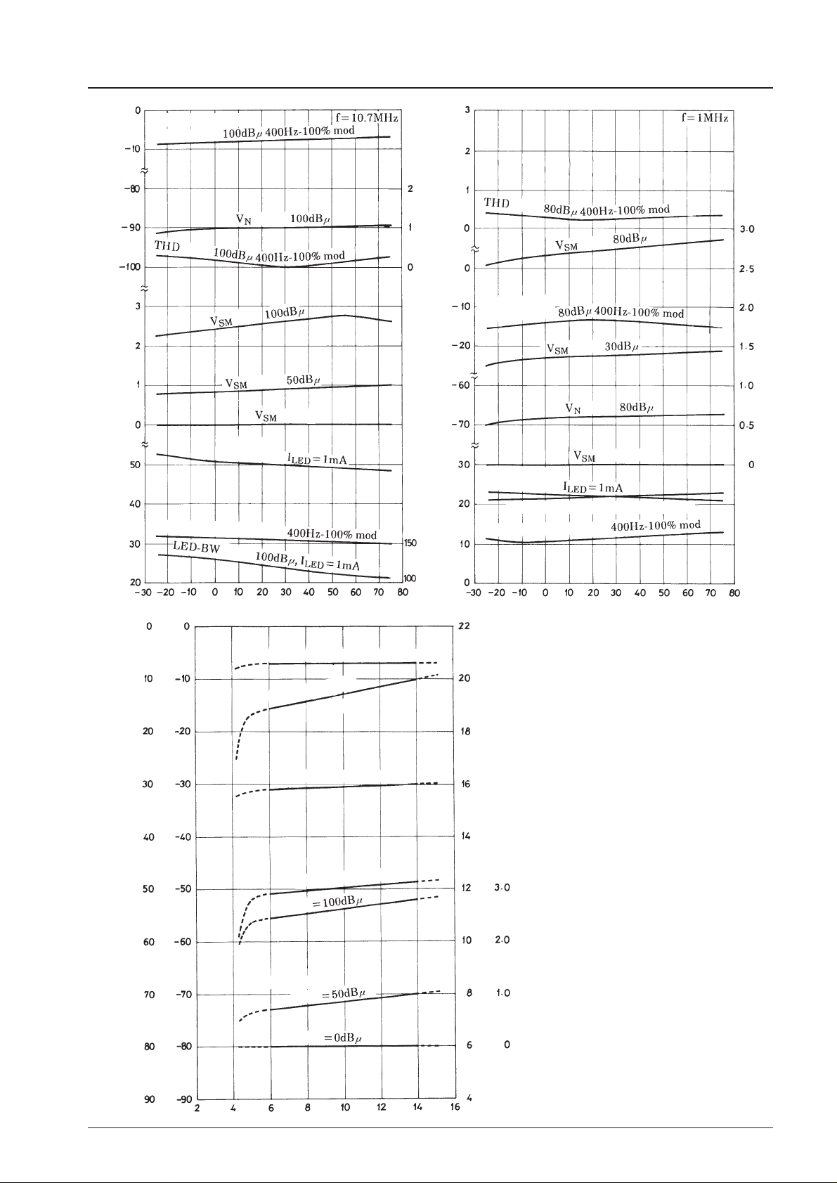
Ambient temperature, Ta – °C
Supply voltage, VCC– V
Ambient temperature, Ta – °C
FM Temperature Characteristics
FM V
CC
Characteristics
AM Temperature Characteristics
Sensitivity – dBµ
Detection output – dBm
Sensitivity – dBµ
S meter voltage, V
SM
– V
Current drain, I
CC
– mA
Total harmonic distortion, THD – %
Total harmonic
distortion,THD – %
Bandwidth, LED-BW – kHz
Sensitivity – dBµ
Noise voltage, V
N
– dBm Detection output – dBm
S meter voltage, V
SM
– V
S meter voltage, V
SM
– V
Noise voltage, V
N
– dBm
Detection output – dBm
Detection output
Input
input
input
input
Detection output
input
input
input
no input
S/N=20dB sensitivity 400Hz-100% mod.
Output 20mV sensitivity
LED lighting
sensitivity
input
input
input
no input
Detection output (Input=100dBµ)
–3dB limiting sensitivity
S meter voltage
Input
LED lighting sensitivity
Input
Input
Current drain, I
CC
No signal
–3dB limiting sensitivity
LED lighting
sensitivity
input
Page 9
LA1265
No.1820-9/15
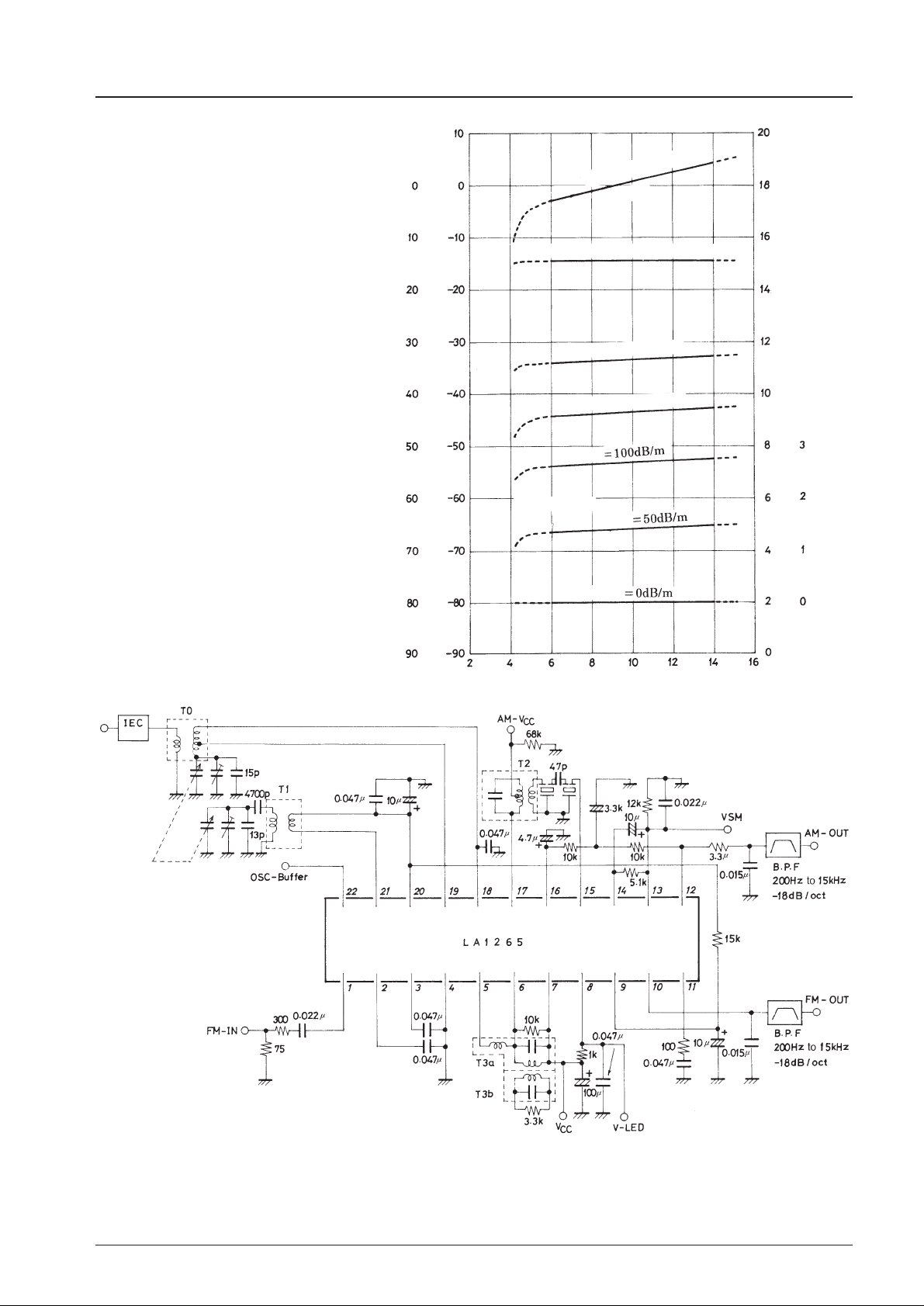
Test Circuit : SW2
Unit (resistance : Ω, capacitance : F)
T0 : YT-30177 (Mitsumi)
T1 : HW-40184 (Mitsumi)
T2 : HW-40174 (Mitsumi)
T3a : HW-40130, T3b : HW-40131 (Mitsumi)
Variable capacitor PVC 22KTL (Mitsumi)
Supply voltage, VCC– V
AM VCCCharacteristics
Detection output – dB
Sensitivity – dBm
S meter voltage, V
SM
– V
Current drain, I
CC
– mA
Current drain, I
CC
No signal
Detection output (Input=100dBµ)
Output 20V sensitivity
LED lighting sensitivity
Input
Input
S meter voltage
Input
Dummy
Page 10
LA1265
No.1820-10/15
IEC input voltage – dBµ
Detection output
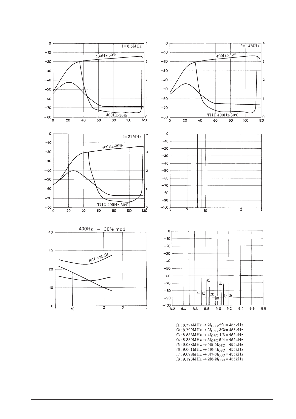
SW2 Input/Output Characteristics
Noise voltage, Detection output – dBm
Total harmonic distortion, THD – %
IEC input voltage – dBµ
SW2 Input/Output Characteristics
Noise voltage, Detection output – dBm
Receiving frequency, fr– MHz
Usable
sensitivity
Image
sensitivity
Max. sensitivity
Input at detection
output 20mV
Image interference – dB Sensitivity – dBµ
Frequency, f – Hz
8.5MHz Spurious Characteristics
Spurious – dB
Receiving frequency
Image frequency
Total harmonic distortion, THD – %
IEC input voltage – dBµ
Detection output
SW2 Input/Output Characteristics
Noise voltage, Detection output – dBm
Total harmonic distortion, THD – %
Noise
voltage
Noise
voltage
Detection output
Noise
voltage
Detection output
Referenced to output –20dBm
Receiving frequency, fr– MHz
8.5 to 9.4MHz Spurious Characteristics
Spurious – dB
Receiving frequency
Image frequency
Referenced to output –20dBm
Page 11
LA1265
No.1820-11/15
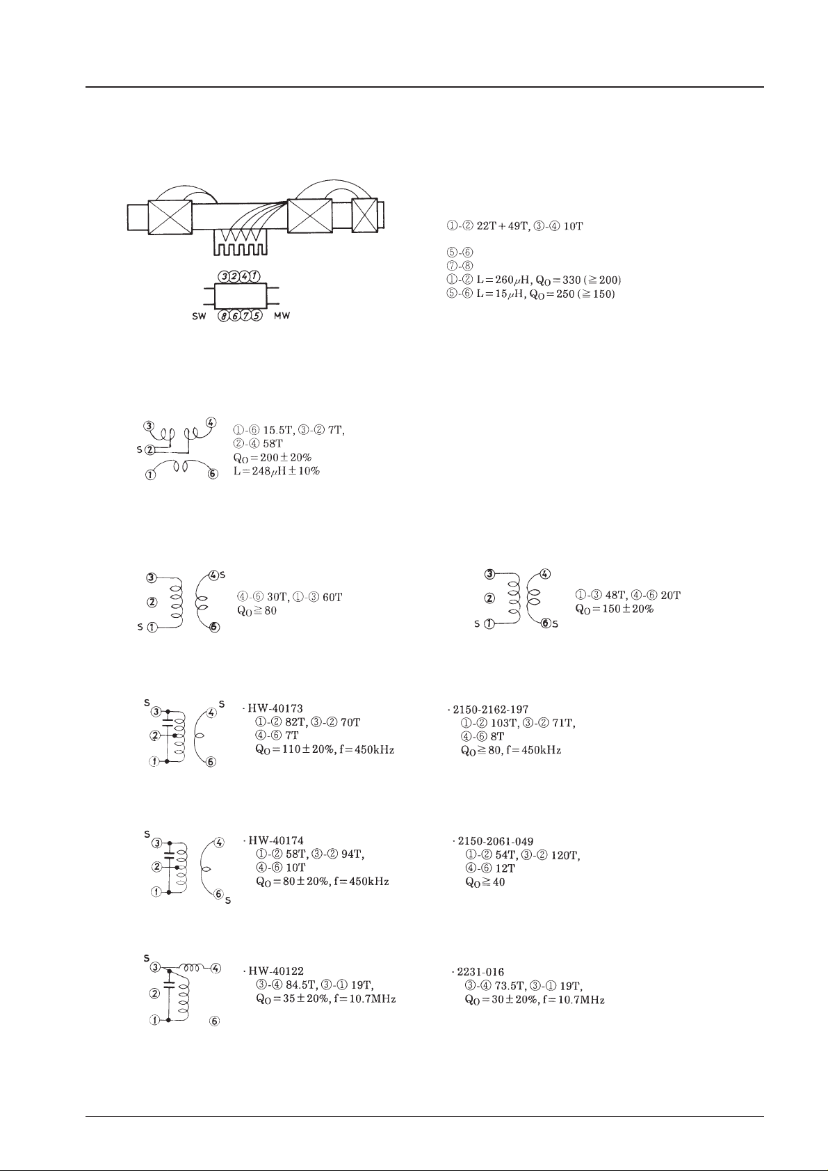
Coil Specifications
MW antenna
Bar antenna (for PVC22KTL)
• TN-10896 (Mitsumi)
Tight solenoid direct winding
17T 0.5φ space winding
4T tight solenoid winding
Loop antenna (for SVC321)
• LA300 (Korin Giken)
Loop antenna matching coil
• KT-412
MW OSC
• 4147-1457-177 (Sumida)
For PVC22KTL
• KO-387 (Korin Giken)
For SVC321
AM-IFT
Matching coil for SFU450B (1-element type)
Matching coil for SFZ450B (2-element type)
FM single tuning detection coil
(Mitsumi)
Internal 180pF
(Sumida)
Internal 180pF
(Mitsumi)
Internal 180pF
(Sumida)
Internal 180pF
(Mitsumi)
Internal 82pF±10%
Damping resistance
Internal 82pF±10%
Damping resistance
(Sumida)
Page 12
LA1265
No.1820-12/15
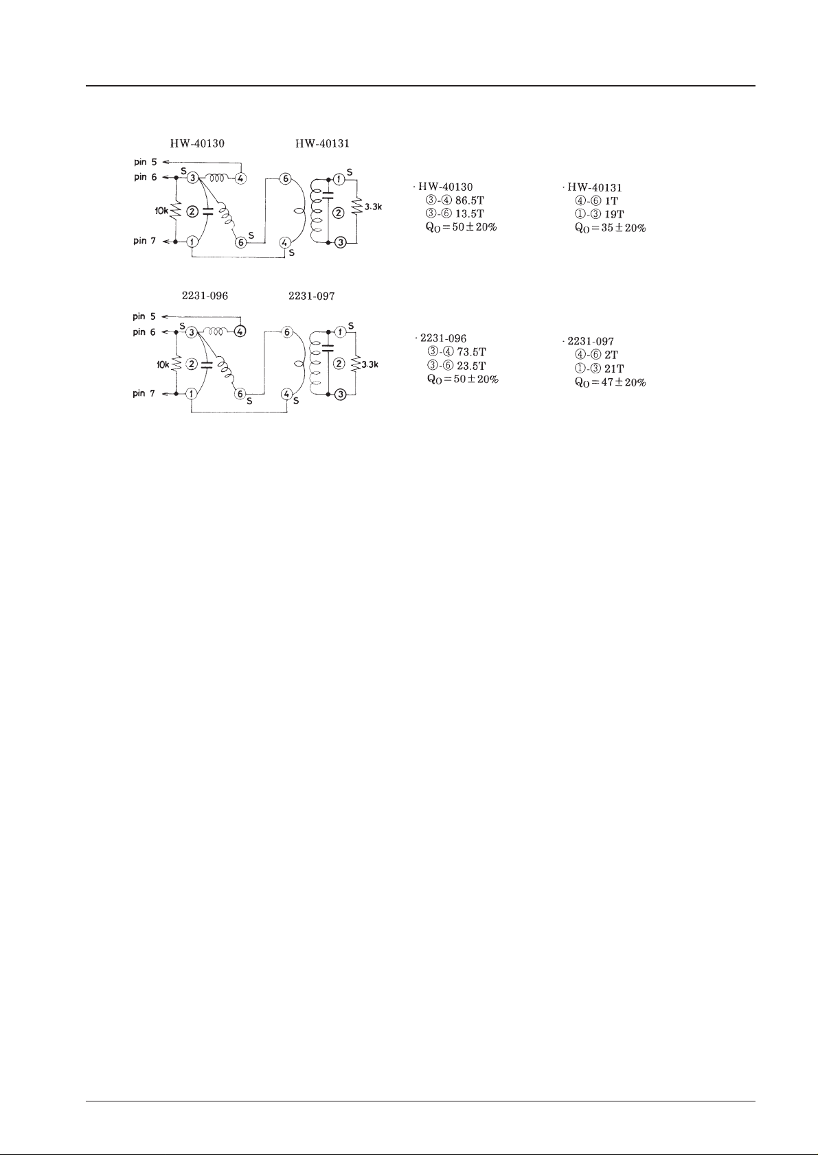
FM double tuning detection coil
(Mitsumi) (Mitsumi)
Internal 100pF±10% Internal 100pF±10%
(Sumida)
(Sumida)
Internal 62pF±10%
Unit (resistance : Ω)
Internal 82pF±10%
Page 13
LA1265
No.1820-13/15
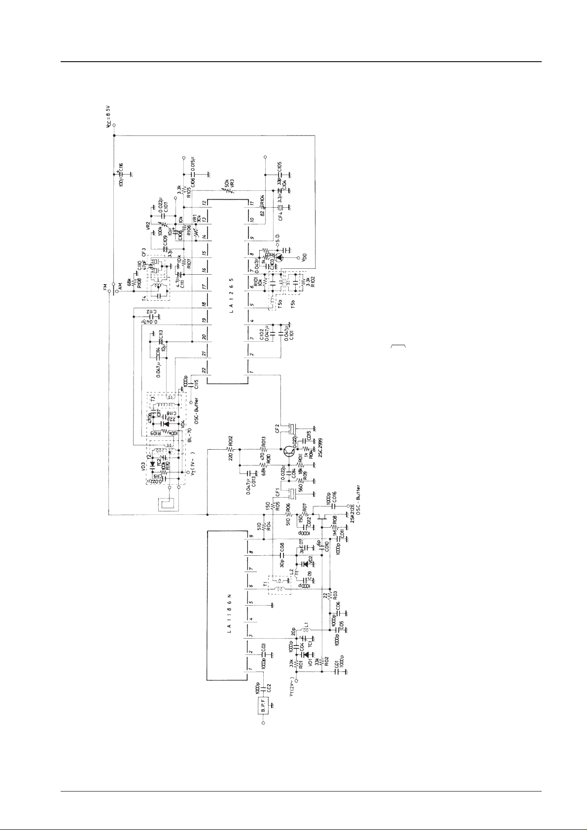
Sample Application Circuit : LA1186N + LA1265 (US Band)
Unit (resistance : Ω, capacitance : F)
B.P. F SNY-2101 (Sumida) T1 : YT-30224 (Mitsumi)
V
D
1, V
D
2=SVC201 T2 : KL412 (Korin) BL-70
V
D
3, V
D
4=SVC321 T3 : KO387 (Korin)
TC1=20pF T4 : HW-40174 (Mitsumi), 2150-2061-049 (Sumida)
TC2=20pF T5a : HW-40130 (Mitsumi), 2231-096 (Sumida)
CF1, CF2=SFE10.7MA T5b: HW-40130 (Mitsumi), 2231-096 (Sumida)
CF3=SFZ450B (Murata)
CF4=BFU450CN (Murata)
L1 : YT-30196 (Mitsumi), 0708-700 (Sumida)
L2 : HW50433 (Mitsumi), 0267-034 (Sumida)
Page 14
LA1265
No.1820-14/15
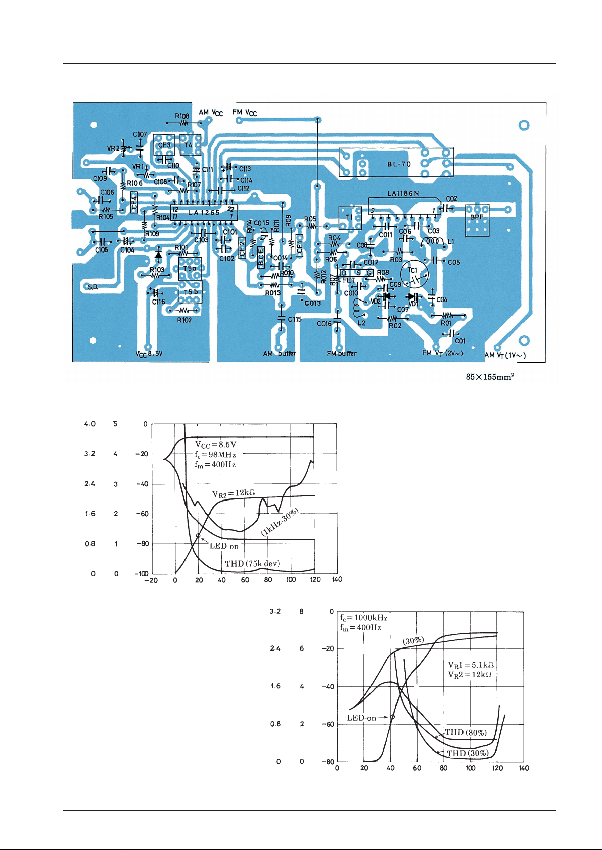
Sample Printed Circuit Pattern (Cu-foiled area)
LA1186+LA1265 Overall Characteristics
Input – dBµ
Detection output (75k dev)
Signal meter
Noise voltage
AM output
Noise voltage, AM output, Detection output – dBm
Total harmonic distortion, THD – %
Signal meter – V
LA1186+LA1265 Overall Characteristics
Input – dB/m
Detection output
Signal meter
Noise voltage
Noise voltage, AM output, Detection output – dBm
Total harmonic distortion, THD – %
Signal meter – V
Page 15

LA1265
No.1820-15/15
No products described or contained herein are intended for use in surgical implants, life-support systems,
aerospace equipment, nuclear power control systems, vehicles, disaster/crime-prevention equipment and
the like, the failure of which may directly or indirectly cause injury, death or property lose.
Anyone purchasing any products described or contained herein for an above-mentioned use shall:
Accept full responsibility and indemnify and defend SANYO ELECTRIC CO., LTD., its affiliates,
subsidiaries and distributors and all their officers and employees, jointly and severally, against any
and all claims and litigation and all damages, cost and expenses associated with such use:
Not impose any responsibilty for any fault or negligence which may be cited in any such claim or
litigation on SANYO ELECTRIC CO., LTD., its affiliates, subsidiaries and distributors or any of
their officers and employees jointly or severally.
Information (including circuit diagrams and circuit parameters) herein is for example only; it is not guaranteed for volume production. SANYO believes information herein is accurate and reliable, but no guarantees
are made or implied regarding its use or any infringements of intellectual property rights or other rights of
third parties.
This catalog provides information as of November, 1997. Specifications and information herein are subject
to change without notice.
 Loading...