

Page 1
tm
October 2006
FDS8949
Dual N-Channel Logic Level PowerTrench® MOSFET
40V, 6A, 29mΩ
Features
Max r
Max r
Low gate charge
High performance trench technology for extremely low
r
DS(on)
High power and current handling capability
RoHS compliant
DS(on)
DS(on)
= 29mΩ at V
= 36mΩ at V
D2
D1
D1
GS
GS
D2
= 10V
= 4.5V
General Description
These N-Channel Logic Level MOSFETs are produced
using Fairchild Semiconductor’s advanced
PowerTrench® process that has been especially tailored
to minimize the on-state resistance and yet maintain
superior switching performance.
These devices are well suited for low voltage and
battery powered applications where low in-line power
loss and fast switching are required.
Applications
Inverter
Power suppliers
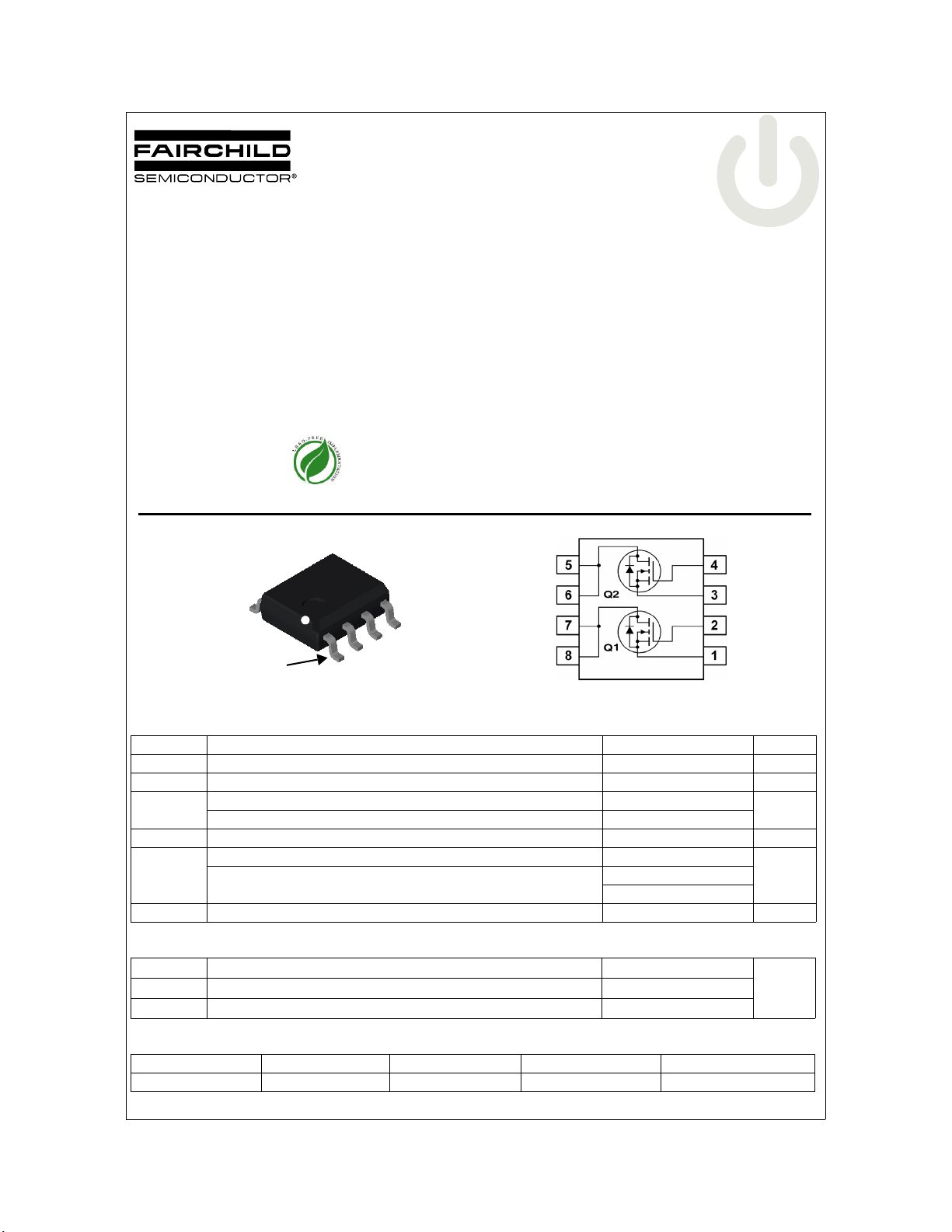
FDS8949 Dual N-Channel Logic Level PowerTrench
SO-8
Pin 1
S1
MOSFET Maximum Ratings T
Symbol Parameter Ratings Units
V
DS
V
GS
I
D
E
AS
P
D
, T
T
J
STG
Drain to Source Voltage 40 V
Gate to Source Voltage ±20 V
Drain Current -Continuous (Note 1a) 6
-Pulsed 20
Drain-Source Avalanche Energy (Note 3) 26 mJ
Power Dissipation for Dual Operation 2
Power Dissipation for Single Operation (Note 1a)
(Note 1b)
Operating and Storage Junction Temperature Range -55 to 150 °C
G2
S2
G1
= 25°C unless otherwise noted
A
1.6
0.9
Thermal Characteristics
R
θJA
θJA
R
θJC
Thermal Resistance-Single operation, Junction to Ambient (Note 1a) 81
Thermal Resistance-Single operation, Junction to Ambient (Note 1b) 135
Thermal Resistance, Junction to Case (Note 1) 40
Package Marking and Ordering Information
Device Marking Device Reel Size Tape Width Quantity
FDS8949 FDS8949 13’’ 12mm 2500 units
®
MOSFET
A
W
°C/WR
©2006 Fairchild Semiconductor Corporation
FDS8949 Rev. B1
www.fairchildsemi.com1
Page 2
Electrical Characteristics T
= 25°C unless otherwise noted
J
Symbol Parameter Test Conditions Min Typ Max Units
FDS8949 Dual N-Channel Logic Level PowerTrench
Off Characteristics
BV
∆BV
∆T
I
DSS
I
GSS
DSS
DSS
J
Drain to Source Breakdown Voltage ID = 250µA, VGS = 0V 40 V
Breakdown Voltage Temperature
Coefficient
Zero Gate Voltage Drain Current
Gate to Source Leakage Current VGS = ±20V,V
On Characteristics
V
GS(th)
∆V
∆T
r
DS(on)
g
FS
GS(th)
J
Gate to Source Threshold Voltage VGS = VDS, ID = 250µA 1 1.9 3 V
Gate to Source Threshold Voltage
Temperature Coefficient
Drain to Source On Resistance
Forward Transconductance VDS = 10V,ID = 6A 22 S
(Note 2)
Dynamic Characteristics
C
iss
C
oss
C
rss
R
g
Input Capacitance
Output Capacitance 105 140 pF
Reverse Transfer Capacitance 60 90 pF
Gate Resistance f = 1MHz 1.1 Ω
Switching Characteristics
t
d(on)
t
r
t
d(off)
t
f
Q
Q
Q
g
gs
gd
Turn-On Delay Time
Rise Time 5 10 ns
Turn-Off D elay Time 23 37 ns
Fall Time 3 6 ns
Total Gate Charge
Gate to Source Gate Charge 2.4 nC
Gate to Drain “Miller”Charge 2.8 nC
ID = 250µA, referenced to 25°C 33 mV/°C
V
= 32V, V
DS
= 0V 1 µA
GS
TJ = 55°C 10 µA
= 0V ±100 nA
DS
ID = 250µA, referenced to 25°C -4.6 mV/°C
VGS = 10V, ID = 6A 21 29
mΩVGS = 4.5V, ID = 4.5A 26 36
VGS = 10V, ID = 6A,TJ = 125°C 29 43
VDS = 20V, VGS = 0V,
715 955 pF
f = 1MHz
VDD = 20V, ID = 1A
VGS = 10V, R
GEN
= 6Ω
9 18 ns
7.7 11 nC
VDS = 20V, ID = 6A,VGS = 5V
®
MOSFET
Drain-Source Diode Characteristics
V
SD
t
rr
Q
rr
Notes:
1: R
θJA
drain pins. R
2: Pulse Test: Pulse Width < 300 us, Duty Cycle < 2.0%.
3: Starting T
FDS8949 Rev. B1 www.fairchildsemi.com2
Source to Drain Diode Forward Voltage V
Reverse Recovery Time (note 3)
Reverse Recovery Charge 7 11 nC
is the sum of the junction-to-case and case-to- ambient thermal resistance where the case thermal reference is defined as the solder mounting surface of the
is guaranteed by design while R
θJC
= 25°C, L = 1mH, IAS = 7.3A, VDD = 40V, VGS = 10V.
J
is determined by the user’s board design.
θJA
a) 81°C/W wh en
mounted on a 1in
pad of 2 oz copper
Scale 1:1 on letter size paper
and Maximum Ratings
= 0V, IS = 6A (note 2) 0.8 1.2 V
GS
IF = 6A, diF/dt = 100A/µs
2
17 26 ns
b) 135°C/W when mounted on a
minimum pad .
Page 3

FDS8949 Dual N-Channel Logic Level PowerTrench
Typical Characteristics T
= 25°C unless otherwise noted
J
20
V
= 10V
GS
16
V
= 4.5V
GS
12
8
4
, DRAIN CURRENT (A)
D
I
0
0.0 0.5 1.0 1.5 2.0 2.5
V
, DRAIN TO SOURCE VOLTAGE (V)
DS
PULSE DURATI ON = 30 0µs
DUTY CYCLE = 20%MAX
Figure 1. On Region Characteristics
1.6
ID = 6A
V
= 10V
GS
1.4
1.2
1.0
NORMALIZED
0.8
0.6
DRAIN TO SOURCE ON-RESISTANCE
-50 -25 0 25 50 75 100 125 150
TJ, JUNCTION TEMPERATURE (oC)
3.0
V
= 3.5V
GS
2.5
2.0
NORMALIZED
1.5
V
= 3.0V
GS
1.0
DRAIN TO SOURCE ON-RESISTANCE
0.5
048121620
Figure 2. Normalized
PULSE DURATION = 300µs
DUTY CYCLE = 20%MAX
VGS = 3.0V
ID, DRAIN CURRENT(A)
V
= 3.5V
GS
VGS = 4.5V
VGS = 10V
On-Resistance vs Drain
Current and Gate Voltage
70
60
(mΩ)
ID = 3.5A
50
40
, DRAIN TO
30
DS(on)
r
20
SOURCE ON-RESISTANCE
10
246810
VGS, GATE TO SOURCE VOLTAGE (V)
PULSE DURATION = 300µs
DUTY CYCLE = 20%MAX
TJ = 125oC
o
T
= 25
C
J
®
MOSFET
Figure 3.
Normalized On Resistance vs Junction
Temperature
20
PULSE DURATION = 300µs
DUTY CYCLE = 20%MAX
16
V
= 10V
DD
12
8
, DRAIN CURRENT (A)
D
I
4
0
1.5 2.0 2.5 3.0 3.5 4.0
VGS, GATE TO SOURCE VOLTAGE (V)
TJ = 125oC
TJ = 25oC
TJ = -55oC
Figure 5. Transfer Characteristics
FDS8949 Rev. B1 www.fairchildsemi.com3
Figure 4.
On-Resistance vs Gate to Source
Voltage
100
V
= 0V
GS
10
TJ = 125oC
1
0.1
0.01
, REVERSE DRAIN CURRENT (A)
S
I
1E-3
0.2 0.4 0.6 0.8 1.0 1.2
VSD, BODY DIODE FORWARD VOLTAGE (V)
Figure 6.
Source to Drain Diode Forw ard
TJ = 25oC
TJ = -55oC
Voltage vs Source Current
Page 4

FDS8949 Dual N-Channel Logic Level PowerTrench
Typical Characteristics T
10
V
DD
= 25°C unless otherwise noted
J
= 10V
8
VDD = 20V
6
4
VDD = 30V
2
, GATE TO SOURCE VOLTAGE(V)
0
GS
V
0481216
Figure 7.
Qg, GATE CHARGE(nC)
Gate Charge Characteristics Figure 8.
10
1
, AVALANCHE CURRENT(A)
AS
I
0.1
10-310-210
TJ = 125oC
-1
tAV, TIME IN AVALANCHE(ms)
10010110210
TJ = 25oC
3
10
C
iss
C
2
10
oss
C
rss
CAPACITANCE (pF)
f = 1MHz
= 0V
V
1
10
0.1 1 10
VDS, DRAIN TO SOURCE VOLTAGE (V)
GS
40
Capacitance vs Drain to Source Voltage
7
6
5
4
3
V
= 4.5V
GS
2
, DRAIN CURRENT (A)
D
1
I
R
= 81oC/W
θJA
3
0
25 50 75 100 125 150
TA, Ambient TEMPER ATU RE (oC)
V
= 10V
GS
®
MOSFET
Figure 9.
Unclamped Inductive Switching
Capability
100
10
1
LIMITED BY
PACKAGE
0.1
OPERATION IN THIS
, DRAIN CURRENT (A)
D
AREA MAY B E
I
LIMITED BY r
0.01
0.01 0.1 1 10 100
DS(on)
SINGLE PULSE
TJ = MAX RATED
T
= 25oC
A
VDS, DRAIN-SOURCE VOLTAGE (V)
Figure 11.
FDS8949 Rev. B1 www.fairchildsemi.com4
Forward Bias Safe Operating Area Figure 12. Single Pulse Maximum Power
100us
1ms
10ms
100ms
1s
10s
DC
300
Figure 10.
Maximum Continuous Drain Current vs
Ambient Temperature
100
10
SINGLE PULSE
1
), PEAK TRANSIENT POWER (W)
PK
0.7
P(
10-410-310-210-110010110210
VGS = 10V
t, PULSE WIDTH (s)
Dissipation
SINGLE PULSE
= 135°C/W
R
θJA
= 25°C
T
A
3
Page 5

FDS8949 Dual N-Channel Logic Level PowerTrench
Typical Characteristics T
2
DUTY CYCLE-DESCENDING ORDER
1
D = 0.5
0.2
0.1
θJA
0.05
0.1
0.02
0.01
0.01
IMPEDANCE, Z
NORMALIZED THERMAL
-3
10
SINGLE PULSE
-2
10
Figure 13. Transient Thermal Response Curve
1E-3
= 25°C unless otherwise noted
J
-1
10
0
10
t, RECTANGULAR PULSE DURATION (s)
P
(PK)
R
(t) = r(t)*R
θ
JA
R
θ
JA
DUTY FACTOR: D = t1/t
1
10
θ
JA
= 135oC/W TJ-TA =P*R
10
t
1
t
2
θ
2
2
JA
3
10
®
MOSFET
FDS8949 Rev. B1 www.fairchildsemi.com5
Page 6

TRADEMARKS
The following are registered and unregistered trademarks Fairchild Semiconductor owns or is authorized to use and is not
intended to be an exhaustive list of all such trademarks.
ACEx™
ActiveArray™
Bottomless™
Build it Now™
CoolFET™
CROSSVOLT™
DOME™
EcoSPARK™
2
E
CMOS™
EnSigna™
FACT™
®
FAST
FASTr™
FPS™
FRFET™
FACT Quiet Series™
GlobalOptoisolator™
GTO™
HiSeC™
2
I
C™
i-Lo™
ImpliedDisconnect™
IntelliMAX™
ISOPLANAR™
LittleFET™
MICROCOUPLER™
MicroFET™
MicroPak™
MICROWIRE™
MSX™
MSXPro™
Across the board. Around the world.™
The Power Franchise
®
OCX™
OCXPro™
OPTOLOGIC
®
OPTOPLANAR™
PACMAN™
POP™
Power247™
PowerEdge™
PowerSaver™
PowerTrench
QFET
®
®
QS™
QT Optoelectronics™
Quiet Series™
RapidConfigure™
RapidConnect™
µSerDes™
ScalarPump™
SILENT SWITCHER
SMART START™
SPM™
Stealth™
SuperFET™
SuperSOT™-3
SuperSOT™-6
SuperSOT™-8
SyncFET™
TCM™
TinyBoost™
TinyBuck™
TinyPWM™
TinyPower™
TinyLogic
®
TINYOPTO™
TruTranslation™
UHC™
Programmable Active Droop™
DISCLAIMER
FAIRCHILD SEMICONDUCTOR RESERVES THE RIGHT TO MAKE CHANGES WITHOUT FURTHER NOTICE TO ANY PRODUCTS
HEREIN TO IMPROVE RELIABILITY, FUNCTION OR DESIGN. FAIRCHILD DOES NOT ASSUME ANY LIABILITY ARISING OUT OF THE
APPLICATION OR USE OF ANY PRODUCT OR CIRCUIT DESCRIBED HEREIN; NEITHER DOES IT CONVEY ANY LICENSE UNDER ITS
PATENT RIGHTS, NOR THE RIGHTS OF OTHERS. THESE SPECIFICATIONS DO NOT EXPAND THE TERMS OF FAIRCHILD’S
WORLDWIDE TERMS AND CONDITIONS, SPECIFICALLY THE WARRANTY THEREIN, WHICH COVERS THESE PRODUCTS.
®
UniFET™
UltraFET
VCX™
Wire™
®
FDS8949 Dual N-Channel Logic Level PowerTrench
LIFE SUPPORT POLICY
FAIRCHILD’S PRODUCTS ARE NOT AUTHORIZED FOR USE AS CRITICAL COMPONENTS IN LIFE SUPPORT DEVICES OR SYSTEMS
WITHOUT THE EXPRESS WRITTEN APPROVAL OF FAIRCHILD SEMICONDUCTOR CORPORATION.
As used herein:
1. Life support devices or systems are devices or systems
which, (a) are intended for surgical implant into the body, or
(b) support or sustain life, or (c) whose failure to perform
when properly used in accordance with instructions for use
provided in the labeling, can be reasonably expected to
result in significant injury to the user.
PRODUCT STATUS DEFINITIONS
Definition of Terms
2. A critical component is any component of a life support
device or system whose failure to perform can be
reasonably expected to cause the failure of the life support
device or system, or to affect its safety or effectiveness.
Datasheet Identification Product Status Definition
Advance Information Formative or In
Design
This datasheet contains the design specifications for
product development. Specifications may change in
any manner without notice.
Preliminary First Production This datasheet contains preliminary data, and
supplementary data will be published at a later date.
Fairchild Semiconductor reserves the right to make
changes at any time without notice in order to improve
design.
No Identification Needed Full Production This datasheet contains final specifications. Fairchild
Semiconductor reserves the right to make changes at
any time without notice in order to improve design.
Obsolete Not In Production This datasheet contains specifications on a product
that has been discontinued by Fairchild semiconductor.
The datasheet is printed for reference information only.
Rev. I20
®
MOSFET
FDS8949 Rev. B1
6
www.fairchildsemi.com
 Loading...