

Page 1
FDS86141
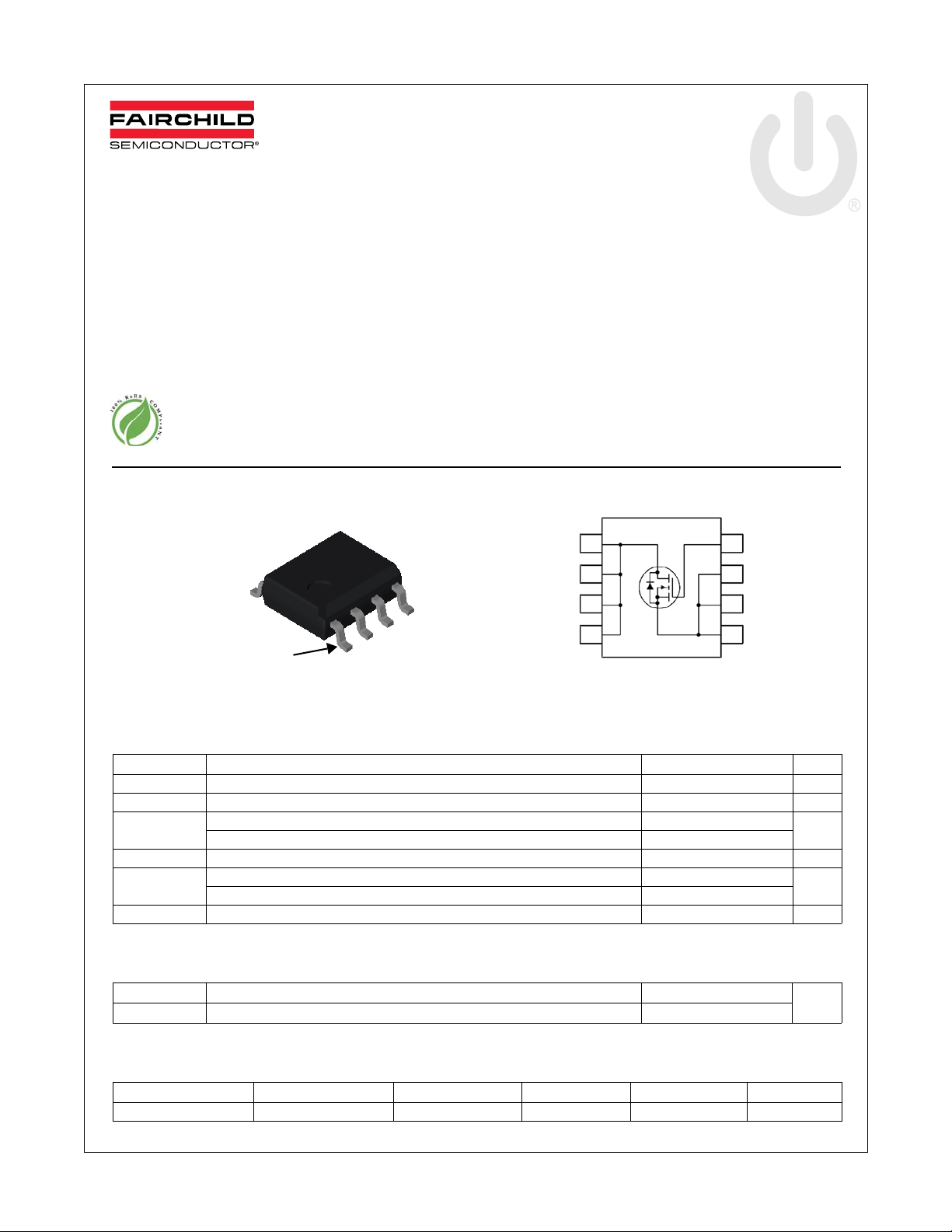
SO-8
D
D
D
D
S
S
S
G
Pin 1
G
S
S
S
D
D
D
D
5
6
7
8
3
2
1
4
N-Channel PowerTrench® MOSFET
100 V, 7 A, 23 m
Features
Maximum R
Maximum R
High-Performance Trench Technology; Extremely Low R
100% UIL Tested
RoHS Compliant
= 23 m at VGS = 10 V, ID = 7 A
DS(on)
= 36 m at VGS = 6 V, ID = 5.5 A
DS(on)
DS(on)
General Description
This N-channel MOSFET is produced using Fairchild
Semiconductor‘s advanced PowerTrench
been especially tailored to minimize the on-state resistance and
maintain superior switching performance.
Applications
DC-DC Conversion
August 2011
®
process that has
FDS86141 — N-Channel PowerTrench
®
MOSFET
MOSFET Maximum Ratings T
Symbol Parameter Ratings Units
V
DS
V
GS
I
D
E
AS
P
D
, T
T
J
STG
Thermal Characteristics
R
JC
R
JA
Package Marking and Ordering Information
Device Marking Device Package Reel Size Tape Width Quantity
FDS86141 FDS86141 SO-8 13 ’’ 12 mm 2500 units
© 2007 Fairchild Semiconductor Corporation
FDS86141 • Rev. C4
Drain to Source Voltage 100 V
Gate to Source Voltage ±20 V
Drain Current -Continuous 7
-Pulsed 30
Single Pulse Avalanche Energy (Note 3) 121 mJ
Power Dissipation TA = 25 °C (Note 1a) 5.0
Power Dissipation T
Operating and Storage Junction Temperature Range -55 to +150 °C
Thermal Resistance, Junction to Case (Note 1) 2.5
Thermal Resistance, Junction to Ambient (Note 1a) 50
= 25 °C unless otherwise noted
A
= 25 °C (Note 1b) 2.5
A
1
A
W
°C/W
www.fairchildsemi.com
Page 2
FDS86141 — N-Channel PowerTrench
Electrical Characteristics T
= 25 °C unless otherwise noted.
J
Symbol Parameter Test Conditions Min. Typ. Max. Units
Off Characteristics
BV
BV
T
I
DSS
I
GSS
DSS
DSS
J
Drain-to-Source Breakdown Voltage ID = 250 A, VGS = 0 V 100 V
Breakdown Voltage Temperature
Coefficient
Zero Gate Voltage Drain Current VDS = 80 V, V
Gate-to-Source Leakage Current VGS = ±20 V, V
I
= 250 A, referenced to 25°C 67 mV/°C
D
= 0 V 1 A
GS
= 0 V ±100 nA
DS
On Characteristics
V
GS(th)
V
T
r
DS(on)
g
FS
GS(th)
J
Gate-to-Source Threshold Voltage VGS = VDS, ID = 250 A23.14V
Gate-to-Source Threshold Voltage
Temperature Coefficient
Static Drain to Source On Resistance
I
= 250 A, Referenced to 25°C -10 mV/°C
D
V
= 10 V, ID = 7 A 19 23
GS
= 6 V, ID = 5.5 A 27 37
GS
= 10 V, ID = 7 A, TJ = 125°C 33 40
V
GS
Forward Transconductance VDS = 10 V, ID = 7 A 19 S
Dynamic Characteristics
C
iss
C
oss
C
rss
R
g
Input Capacitance
Output Capacitance 186 247 pF
Reverse Transfer Capacitance 8.6 13 pF
Gate Resistance 0.5
Switching Characteristics
t
d(on)
t
r
t
d(off)
t
f
Q
g(TOT)
Q
gs
Q
gd
Turn-On Delay Time
Rise Time 3.2 10 ns
Turn-Off Delay Time 14.3 26 ns
Fall Time 3.2 10 ns
Total Gate Charge VGS = 0 V to 10 V
Total Gate Charge V
Total Gate Charge 3.4 nC
Gate to Drain “Miller” Charge 3.1 nC
= 50 V, VGS = 0 V,
V
DS
f = 1 MHz
= 50 V, ID = 7 A,
V
DD
V
= 10 V, R
GS
= 0 V to 5 V 6.7 9.4 nC
GS
GEN
= 6
V
DD
I
= 7 A
D
= 50 V
703 934 pF
8.3 17 ns
11.8 16.5 nC
mV
®
MOSFET
Drain-Source Diode Characteristics
V
SD
t
rr
Q
rr
NOTES:
is determined with the device mounted on a 1 in2 pad 2 oz copper pad on a 1.5 x 1.5 in. board of FR-4 material. R
1. R
JA
the user's board design.
2. Pulse Test: Pulse Width < 300 s, Duty Cycle < 2.0 %.
3. Starting T
© 2007 Fairchild Semiconductor Corporation
FDS86141 • Rev. C4
Source-to-Drain Diode Forward Voltage
Reverse Recovery Time
Reverse Recovery Charge 39 62 nC
= 25 oC; N-ch: L = 3 mH, IAS = 9 A, VDD = 100 V, VGS = 10 V.
J
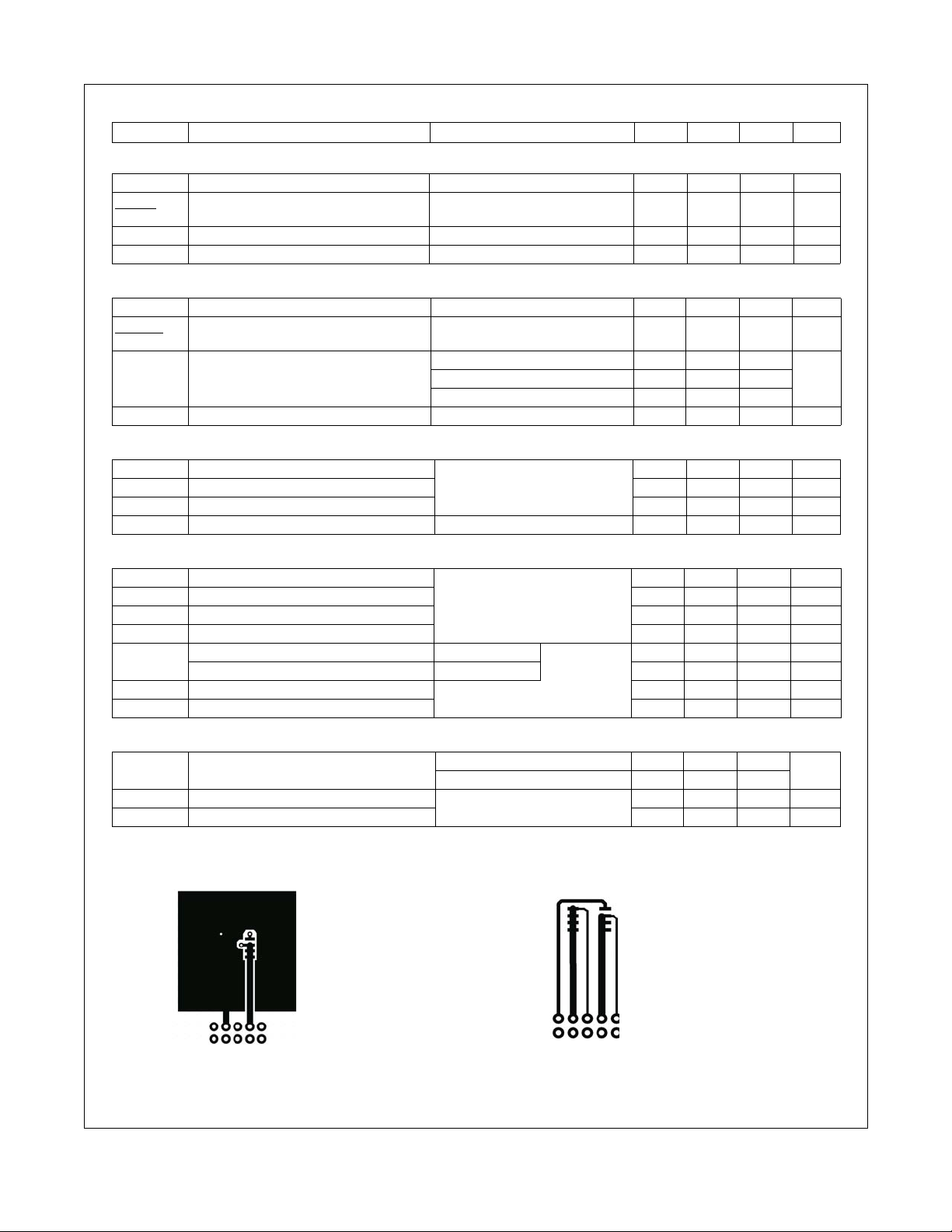
a) 50 °C/W whe n mounted on a
2
1 in
pad of 2 oz copper.
V
= 0 V, IS = 7 A (Note 2) 0.8 1.3
GS
= 0 V, IS = 2 A (Note 2) 0.8 1.2
V
GS
= 7 A, di/dt = 100 A/s
I
F
2
JC
43 69 ns
is guaranteed by design while R
b) 125 °C/W when mounted on a
minimum pad.
V
is determined by
CA
www.fairchildsemi.com
Page 3
FDS86141 — N-Channel PowerTrench
0.0 0.5 1.0 1.5 2.0 2.5 3.0
0
5
10
15
20
25
30
VGS = 7 V
VGS = 5.5 V
VGS = 10 V
PULSE DURATION = 80 s
DUTY CYCLE = 0.5% MAX
VGS = 5 V
VGS = 6 V
I
D
, DRAIN CURRENT (A)
V
DS
, DRAIN TO SOURCE VOLTAGE (V)
0 5 10 15 20 25 30
0
1
2
3
4
VGS = 5 V
PULSE DURA TION = 80s
DUTY CYCLE = 0.5% MAX
NORMALIZED
DRAIN TO SOURCE ON-RESISTANCE
I
D
, DRAIN CURRENT (A)
V
GS
= 6 V
VGS = 7 V
VGS = 5.5 V
V
GS
= 10 V
-75 -50 -25 0 25 50 75 100 125 150
0.6
0.8
1.0
1.2
1.4
1.6
1.8
2.0
ID = 7 A
V
GS
= 10 V
NORMALIZED
DRAIN TO SOURCE ON-RESISTANCE
T
J
, JUNCTION TEMPERATURE (
o
C)
45678910
0
20
40
60
80
TJ = 125 oC
ID = 7 A
TJ = 25 oC
V
GS
, GATE TO SOURCE V O L TAGE (V)
r
DS(on)
,
DRAIN TO
SOURCE ON-RESISTANCE
(m)
PULSE DURATION = 80 s
DUTY CYCLE = 0.5% MAX
2468
0
5
10
15
20
25
30
TJ = 150 oC
V
DS
= 5 V
PULSE DURATION = 80 s
DUTY CYCLE = 0.5% MAX
TJ = -55 oC
TJ = 25 oC
I
D
, DRAIN CURRENT (A)
VGS, GATE TO SOURCE VOLTAGE (V)
0.2 0.4 0.6 0.8 1.0 1.2
0.01
0.1
1
10
30
TJ = -55 oC
TJ = 25 oC
TJ = 150 oC
V
GS
= 0 V
I
S
, REVERSE DRAIN CURRENT (A)
VSD, BODY DIODE FORWARD VOLTAGE (V)
Typical Characteristics T
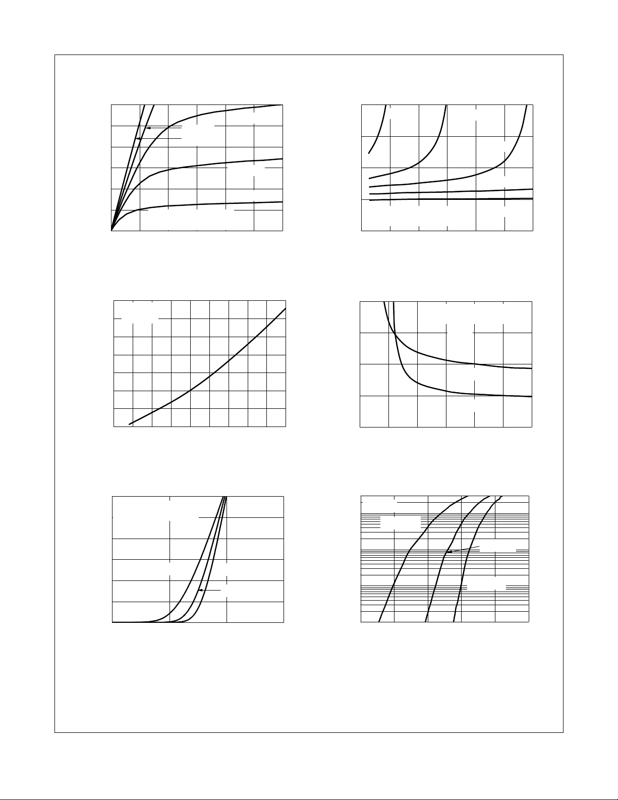
Figure 1 . O n - R e g i o n Characteristics Figure 2. Normalized O n - R e s i s t a n c e
= 25 °C unless otherwise noted.
J
vs. Drain Current and Gate Voltage
®
MOSFET
Figu r e 3 . Norma l i z ed On- R e s i stance
vs. Junction Temperature
© 2007 Fairchild Semiconductor Corporation
FDS86141 • Rev. C4
Figure 5. Transfer Characteristics Figure 6. Source-to-Drain Diode Forward Voltage
Figure 4. On-Resistance vs. Gate-to-Source Voltage
vs. Source Current
3
www.fairchildsemi.com
Page 4
FDS86141 — N-Channel PowerTrench
0 3 6 9 12 15
0
2
4
6
8
10
ID = 7 A
VDD = 50 V
V
DD
= 25 V
V
GS
, GATE TO SOURCE VOLTAGE (V)
Qg, GATE CHARGE (nC)
VDD = 75 V
0.1 1 10 100
5
10
100
1000
f = 1 MHz
V
GS
= 0 V
CAPACITANCE (pF)
VDS, DRAIN TO SOURCE VOLTAGE (V)
C
rss
C
oss
C
iss
0.01 0.1 1 10 50
1
10
20
TJ = 100 oC
TJ = 25 oC
TJ = 125 oC
tAV, TIME IN AVALAN CHE (ms)
I
AS
, AVALANCHE CURRENT (A)
25 50 75 100 125 150
0
2
4
6
8
V
GS
= 6 V
R
JA
= 50 oC/W
V
GS
= 10 V
I
D
, DRAIN CURRENT (A)
T
A
, AMBIENT TEMPERATURE (
o
C)
0.01 0.1 1 10 100 600
0.01
0.1
1
10
100
10 s
100us
10 ms
DC
1 s
100 ms
1 ms
I
D
, DRAIN CURRENT (A)
VDS, DRAIN to SOURCE VOLTAGE (V)
THIS AREA IS
LIMITED BY r
DS(on)
SINGLE PULSE
T
J
= MAX RATED
R
JA
= 125
o
C/W
T
A
= 25
o
C
10
-3
10
-2
10
-1
110
100 1000
0.5
1
10
100
500
SINGLE PULSE
R
JA
= 125
o
C/W
T
A
= 25
o
C
P(
PK
), PEAK TRANSIENT POWER (W)
t, PULSE WIDTH (sec)
Typical Characteristics T
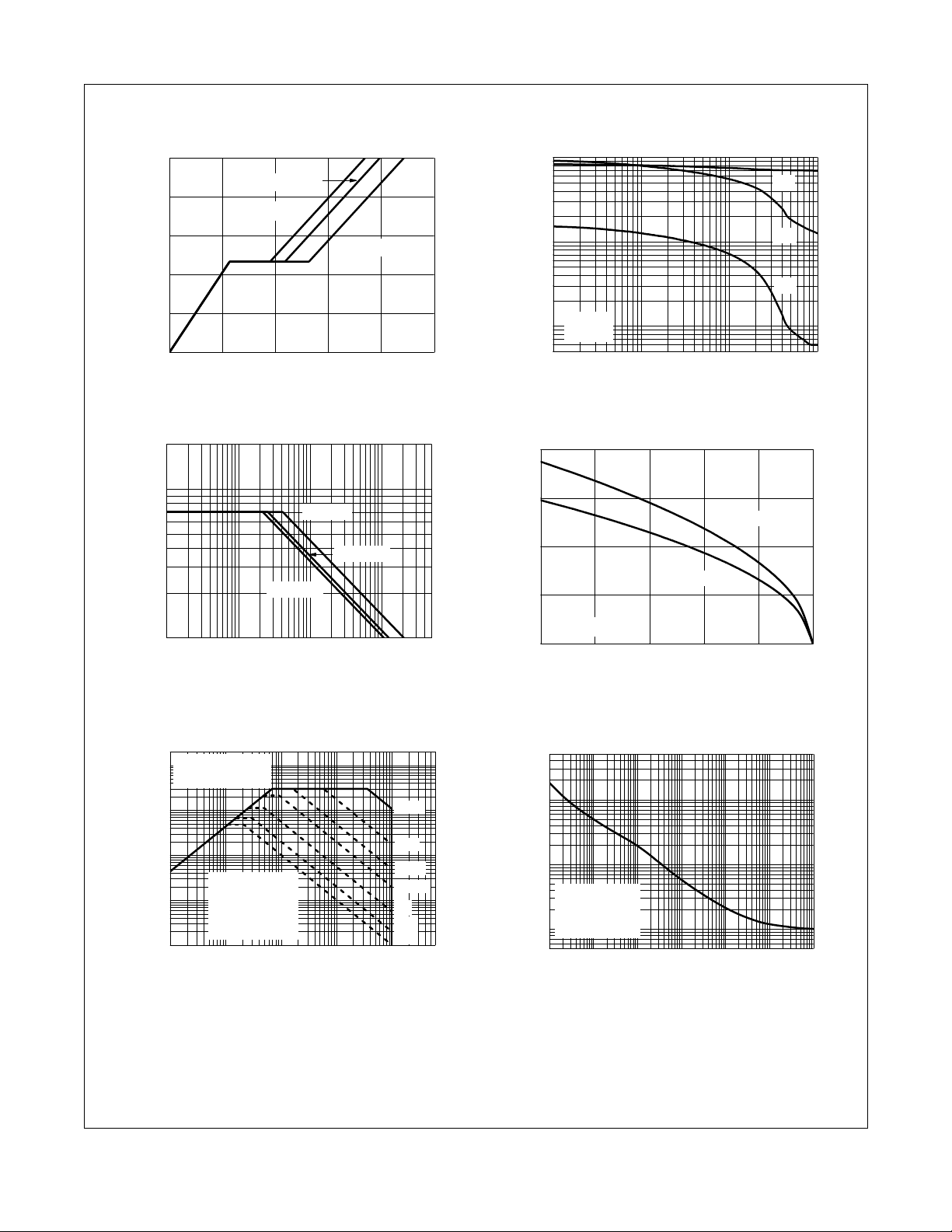
Figure 7. Gate Charge Characteristics Figure 8. Capacitance vs. Drain-to-Source Voltage
= 25 °C unless otherwise noted.
J
®
MOSFET
Figure 9. Unclamped Inductive Switching Capability Figure 10. Maximum Continuous Drain Current
© 2007 Fairchild Semiconductor Corporation
FDS86141 • Rev. C4
Figure 11. Forward Bias Safe Operating Area Figure 12. Single-Pulse Maximum Power Dissipation
vs. Ambient Temperature
4
www.fairchildsemi.com
Page 5
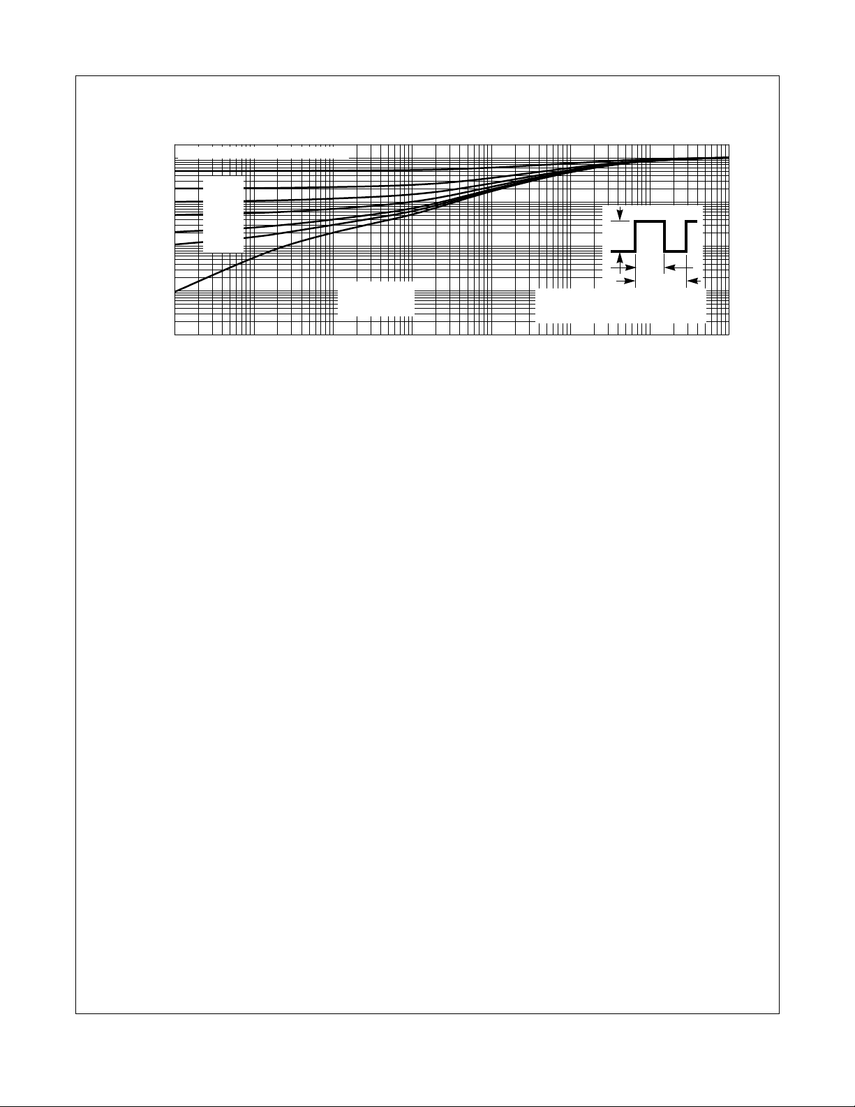
FDS86141 — N-Channel PowerTrench
10
-4
10
-3
10
-2
10
-1
110
100 1000
0.0001
0.001
0.01
0.1
1
2
SINGLE PULSE
R
JA
= 125 oC/W
DUTY CYCLE-DESCENDING ORDER
NORMALIZED THERMAL
IMPEDANCE,
Z
JA
t, RECTANGULAR PULSE DURATION (sec)
D = 0.5
0.2
0.1
0.05
0.02
0.01
P
DM
t
1
t
2
NOTES:
DUTY FACTOR: D = t
1/t2
PEAK TJ = PDM x Z
JA
x R
JA
+ T
A
Typical Characteristics T
Figure 13. Junction-to-Ambient Transient Thermal Response Curve
= 25 °C unless otherwise noted.
J
®
MOSFET
© 2007 Fairchild Semiconductor Corporation
FDS86141 • Rev. C4
5
www.fairchildsemi.com
Page 6
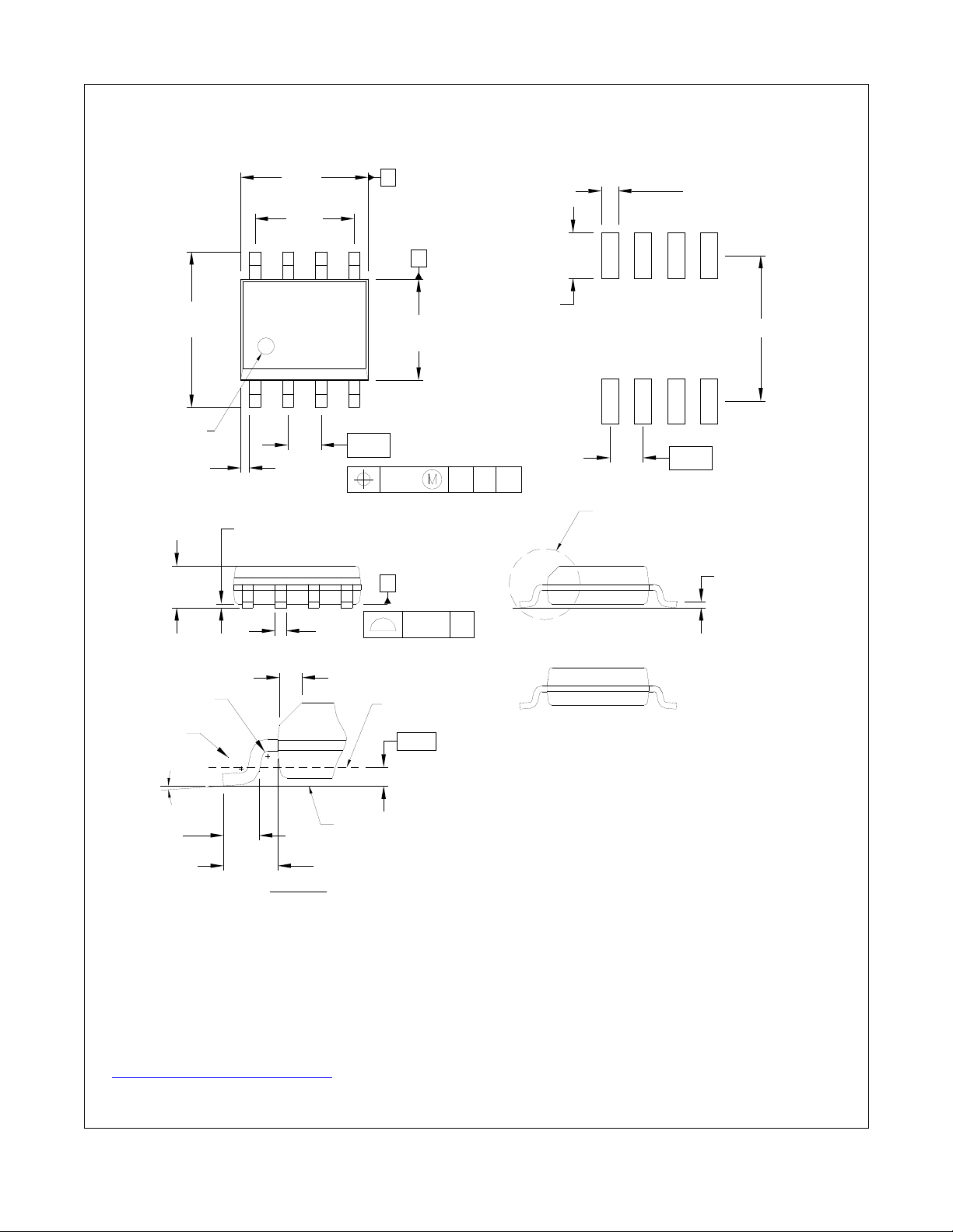
Physical Dimensions
8°
0°
SEE DETAIL A
NOTES: UNLESS OTHERWISE SPECIFIED
A) THIS PACKAGE CONFORMS TO JEDEC
MS-012, VARIATION AA, ISSUE C,
B) ALL DIMENSIONS ARE IN MILLIMETERS.
C) DIMENSIONS DO NOT INCLUDE MOLD
FLASH OR BURRS.
D) LANDPATTERN STANDARD: SOIC127P600X175-8M.
E) DRAWING FILENAME: M08AREV13
LAND PATTERN RECOMMENDATION
SEATING PLANE
C
GAGE PLANE
x 45°
DETAIL A
SCALE: 2:1
PIN ONE
INDICATOR
4
8
1
B
5
A
5.60
0.65
1.75
1.27
6.20
5.80
3.81
4.00
3.80
5.00
4.80
(0.33)
1.27
0.51
0.33
0.25
0.10
1.75 MAX
0.25
0.19
0.36
0.50
0.25
R0.10
R0.10
0.90
0.40
(1.04)
OPTION A - BEVEL EDGE
OPTION B - NO BEVEL EDGE
0.25 CBA
0.10
C
FDS86141 — N-Channel PowerTrench
®
MOSFET
© 2007 Fairchild Semiconductor Corporation
FDS86141 • Rev. C4
Figure 1. 8-Lead, Small-Outline Integrated Circuit (SOIC), JEDEC MS-012, .150" Narrow Body
Package drawings are provided as a service to customers considering Fairchild co mponents. Drawings may change in any manner
without notice. Please note the revision and/or date on the drawing and contact a Fairchild Semiconductor r epresentative to ver ify or
obtain the most recent revision. Package specifications do not expand the terms of Fairchild’s worldwide terms and conditions,
specifically the warranty therein, which covers Fairchild products.
Always visit Fairchild Semiconductor’s online packaging area for the most recent package drawings:
http://www.fairchildsemi.com/packaging/
.
6
www.fairchildsemi.com
Page 7
FDS86141 — N-Channel PowerTrench
®
MOSFET
© 2007 Fairchild Semiconductor Corporation
FDS86141 • Rev. C4
7
www.fairchildsemi.com
 Loading...