

Datasheet FAN2513S285X, FAN2513S27X, FAN2513S26X, FAN2513S25X, FAN2512SX Datasheet (Fairchild Semiconductor)
...Page 1
www.fairchildsemi.com
FAN2512, FAN2513
150 mA CMOS LDO Regulators with Fast Start Enable
Features
• Ultra Low Power Consumption
• Enable optimized for CDMA time phases
• 150 mV dropout voltage at 150 mA
• 25 µA ground current at 150 mA
• Enable/Shutdown Control
• SOT23-5 package
• Thermal limiting
• 300 mA peak current
Applications
• Cellular Phones and accessories
•PDAs
• Portable cameras and video recorders
• Laptop, notebook and palmtop computers
Description
The F AN2512/13 family of micropower lo w-dropout v oltage
regulators utilize CMOS technology to offer a new level of
cost-effective performance in GSM, TDMA, and CDMA
cellular handsets, Laptop and Notebook portable computers,
and other portable devices. Features include extremely low
power consumption and low shutdown current, low dropout
voltage, exceptional loop stability able to accommodate a
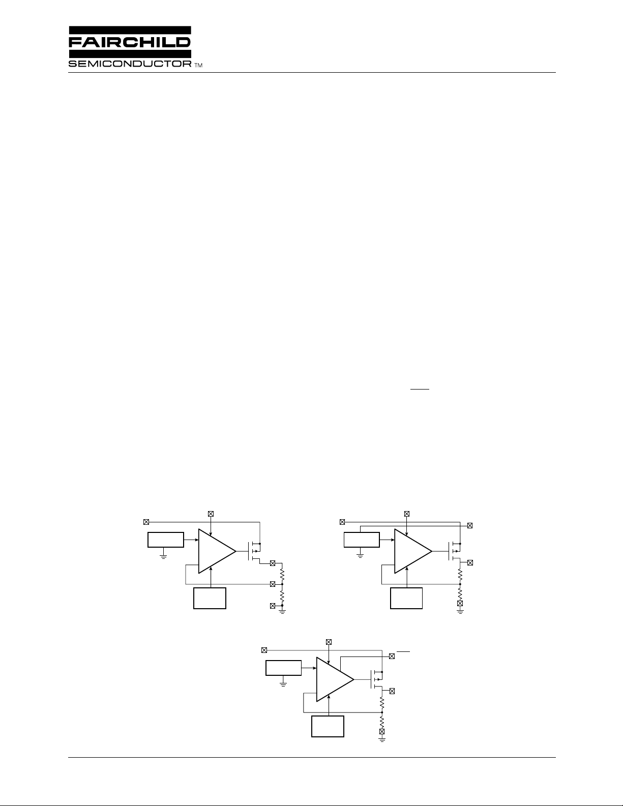
Block Diagrams
EN
V
IN
Bandgap
Error
Amplifier
p
V
OUT
ADJ
wide variety of external capacitors, and the compact SOT23-5
surface-mount package. In addition, the F AN2512/13 f amily
offer the fast power-cycle time required in CDMA handset
applications. These products offer significant improvements
over older BiCMOS designs and are pin-compatible with
many popular devices. The output is thermally protected
against overload.
The FAN2512 and FAN2513 devices are distinguished by
the assignment of pin 4:
FAN2512: pin 4 – ADJ, allowing the user to adjust the
output voltage over a wide range using an external voltage
divider.
FAN2512-XX: pin 4 – BYP, to which a bypass capacitor
may be connected for optimal noise performance. Output
voltage is fixed, indicated by the suffix XX.
FAN2513-XX: pin 4 – ERR
, a flag which indicates that the
output voltage has dropped below the specified minimum
due to a fault condition.
The standard fixed output voltages available are 2.5V, 2.6V,
2.7V, 2.8V , 2.85V, 3.0V , and 3.3V. Custom output voltage are
also available: please contact your local Fairchild Sales
Office for information.
EN
V
IN
Bandgap
Error
Amplifier
p
BYP
V
OUT
FAN2512
Thermal
Sense
GND
V
IN
Bandgap
FAN2513-XX
FAN2512-XX
EN
Error
Amplifier
Thermal
Sense
Thermal
Sense
ERR
p
V
OUT
GND
GND
REV. 1.1.7 2/14/03
Page 2
0:
1:
0:
. 1:
PRODUCT SPECIFICATION FAN2512/FAN2513
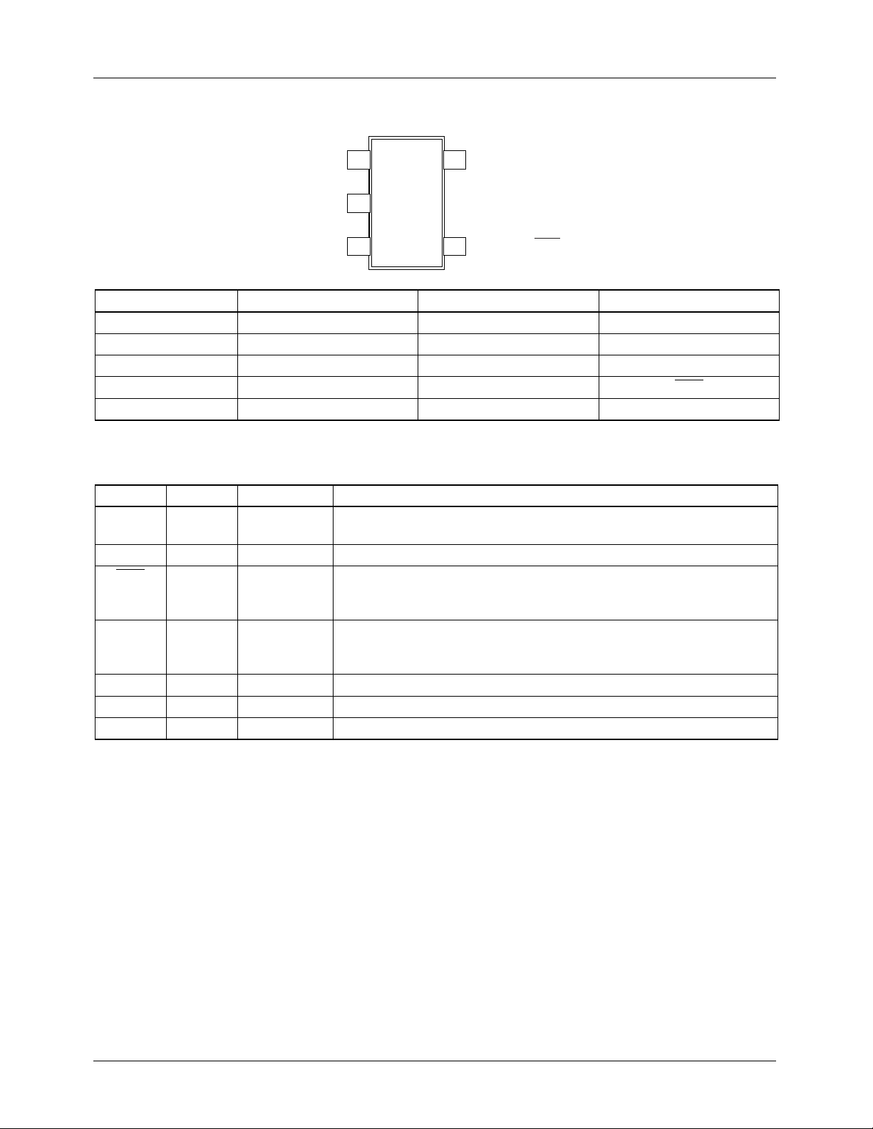
Pin Assignments
15
V
IN
V
OUT
EN
2
3
4
ADJ/BYP/ERR
GND
Pin No. FAN2512 FAN2512-XX FAN2513-XX
1. V
IN
V
IN
2. GND GND GND
3. EN EN EN
4. ADJ BYP ERR
5. V
OUT
V
OUT
Pin Descriptions
Pin Name Pin No. Type Pin Function Description
ADJ 4 Input
BYP 4 Passive
ERR 4 Open drain FAN2513-XX Error. Error flag output.
EN 3 Digital Input Enable.
V
V
IN
OUT
1 Power in
5 Power out
GND 2 Power
FAN2512 Adjust. Ratio of potential divider from VOUT to ADJ
determines output voltage.
FAN2512-XX Bypass. Connect 470 pF capacitor for noise reduction.
Output voltage < 95% of nominal.
Output voltage > 95% of nominal.
Shutdown V
Enable V
OUT
OUT
.
Voltage Input. Supply voltage input.
Voltage Output. Regulated output voltage.
Ground.
V
V
OUT
IN
Functional Description
Designed utilizing CMOS process technology, the
FAN2512/13 family of products are carefully optimized for
use in compact battery-powered devices, offering a unique
combination of low power consumption, extremely low
dropout voltages, high tolerance for a variety of output
capacitors, and the ability to disable the output to less than
1µA under user control. In the circuit, a difference amplifier
controls the current through a series-pass P-Channel
MOSFET, comparing the load voltage at the output with an
onboard low-drift bandgap reference. The series resistance
of the pass P-Channel MOSFET is approximately 1 Ω , resulting in an unusually low dropout voltage under load when
compared to older bipolar pass-transistor designs.
2
Protection circuitry is provided onboard for overload conditions. In conditions where the device reaches temperatures
exceeding the specified maximums, an onboard circuit shuts
down the output, where it remains suspended until it has
cooled before re-enabling. The user is also free to shut down
the device using the Enable control pin at any time.
Careful design of the output regulator amplifier assures loop
stability over a wide range of ESR values in the external
output capacitor. A wide range of values and types can be
accommodated, allowing the user to select a capacitor
meeting his space, cost, and performance requirements,
and enjoy reliable operation over temperature, load, and
tolerance variations.
REV. 1.1.7 2/14/03
Page 3

3
FAN2512/FAN2513 PRODUCT SPECIFICATION
An Enable pin, available on all devices, allows the user to
shut down the regulator output to conserve power, reducing
supply current to less than 1µA. The output can then be
re-Enabled within 500µSec, fulfilling the fast power-c ycling
needs of CDMA applications. Depending on the model
selected, other control and status functions are available at
pin 4 to enhance the operation of the device. The adjustablevoltage versions utilize pin 4 to connect to an external
voltage divider which feeds back to the regulator error
amplifier, thereby setting the voltage as desired. Two other
functions are available in the fixed-voltage versions: in
noise-sensitive applications, an external Bypass capacitor
connection is provided that allows the user to achieve optimal noise performance at the output, while the Error output
functions as a diagnostic flag to indicate that the output
voltage has dropped more than 5% below the nominal fixed
voltage.
Applications Information
External Capacitors – Selection
The FAN2512/13 allows the user to utilize a wide variety of
capacitors compared to other LDO products. An innovative
design approach offers significantly reduced sensitivity to
ESR (Effective Series Resistance), which de grades re gulator
loop stability in older designs. While the improvements featured in the FAN2512/13 family greatly simplify the design
task, capacitor quality still must be considered if the designer
is to achieve optimal circuit performance. In general,
ceramic capacitors offer superior ESR performance, at a
lower cost and a smaller case size than tantalums. Those with
X7R or Y5Vdielectric offer the best temperature coefficient
characteristics. The combination of tolerance and variation
over temperature in some capacitor types can result in significant variations, resulting in unstable performance over rated
conditions.
Input Capacitor
An input capacitor of 2.2µF (nominal value) or greater,
connected between the Input pin and Ground, located in
close proximity to the device, will improve transient
response and noise rejection. Higher values will offer superior input ripple rejection and transient response. An input
capacitor is recommended when the input source, either a
battery or a regulated AC voltage, is located far from the
device. Any good quality ceramic, tantalum, or metal film
capacitor will give acceptable performance, however tantalum capacitors with a surge current rating appropriate to the
application must be selected to avoid catastrophic failure.
Output Capacitor
An output capacitor is required to maintain regulator loop
stability. Unlik e many other LDO regulators, the FAN2512/13
family of products are nearly insensitive to output capacitor
ESR. Stable operation will be achieved with a wide variety
of capacitors with ESR values ranging from 10m Ω to 10 Ω or
more. Tantalum or aluminum electrolytic, or multilayer
ceramic types can all be used. A nominal value of at least
1µF is recommended.
Bypass Capacitor (FAN2512 Only)
In the fixed-voltage configuration, connecting a capacitor
between the bypass pin and ground can significantly reduce
noise on the output. Values ranging from 470pF to 10nF can
be used, depending on the sensitivity to output noise in the
application.
At the high-impedance Bypass pin, care must be taken in the
circuit layout to minimize noise pickup, and capacitors must
be selected to minimize current loading (leakage). Noise
pickup from external sources can be considerable. Leakage
currents into the Bypass pin will directly affect regulator
accuracy and should be kept as low as possible; thus, highquality ceramic and film types are recommended for their
low leakage characteristics. Cost-sensitive applications not
concerned with noise can omit this capacitor.
Control Functions
Enable Pin
Applying a voltage of 0.4V or less at the Enable pin will disable the output, reducing the quiescent output current to less
than 1µA, while a voltage of 2.0V or greater will enable the
device. If this shutdown function is not needed, the pin can
simply be connected to the V
will cause erratic operation.
Error Flag (FAN2513 Only)
To indicate conditions such as input voltage dropout
(low V
), overheating, or overloading (excessive output
IN
current), the ERR pin indicates a fault condition. It is an
open-drain output which is HIGH when the voltage at V
is greater than 95% of the nominal rated output voltage and
LOW when V
is less than 95% or the rated output volt-
OUT
age, as specified in the error trip level characteristics.
A logic pullup resistor of 100K Ω is recommended at this
output. The pin can be left disconnected if unused.
Thermal Protection
The FAN2512/13 is designed to supply high peak output
currents of up to 1A for brief periods, however this output
load will cause the device temperature to increase and
exceed maximum ratings due to power dissipation. During
output overload conditions, when the die temperature
exceeds the shutdown limit temperature of 150°C, onboard
thermal protection will disable the output until the temperature drops below this limit, at which point the output is then
re-enabled. During a thermal shutdown situation the user
may assert the power-down function at the Enable pin,
reducing power consumption to the minimum level I
pin. Allo wing this pin to float
IN
GND
OUT
.
REV. 1.1.7 2/14/03
Page 4

PRODUCT SPECIFICATION FAN2512/FAN2513
Thermal Characteristics
The FAN2512/13 is designed to supply 150mA at the specified output voltage with an operating die (junction) temperature of up to 125°C. Once the power dissipation and thermal
resistance is known, the maximum junction temperature of
the device can be calculated. While the power dissipation is
calculated from known electrical parameters, the thermal
resistance is a result of the thermal characteristics of the
compact SOT23-5 surface-mount package and the surrounding PC Board copper to which it is mounted.
The power dissipation is equal to the product of the input-tooutput voltage differential and the output current plus the
ground current multiplied by the input voltage, or:
P
VINV
D
The ground pin current I
–()I
OUT
OUTVIN
can be found in the charts
GND
provided in the Electrical Characteristics section.
The relationship describing the thermal behavior of the
package is:
T
J max()TA
-------------------------------
P
=
D max()
θ
JA
I
+=
GND
–
device to enter a thermal cycling loop, in which the circuit
enters a shutdown condition, cools, re-enables, and then
again overheats and shuts down repeatedly due to an
unmanaged fault condition.
Operation of Adjustable Version
The adjustable version of the FAN2512/13 includes an input
pin ADJ which allows the user to select an output voltage
ranging from 1.32V to near V
divider . The voltage V
ADJ
the onboard error amplifier which adjusts the output voltage
until V
is equal to the onboard bandgap reference voltage
ADJ
of 1.32V(typ). The equation is:
V
OUT
1.32V 1
The total value of the resistor chain should not exceed
250K Ω total to keep the error amplifier biased during
no-load conditions. Programming output voltages very near
V
need to allow for the magnitude and variation of the
IN
dropout voltage V
over load, supply, and temperature
DO
variations. Note that the low-leakage FET input to the
CMOS Error Amplifier induces no bias current error to the
calculation.
, using an external resistor
IN
presented to the ADJ pin is fed to
R
upper
--------------- -+×=
R
lower
where T
ture of the die, which is 125°C, and T
ing temperature. θ
board layout and can be empirically obtained. While the θ
is the maximum allowable junction tempera-
J(max)
is dependent on the surrounding PC
JA
is the ambient operat-
A
JC
(junction-to-case) of the SOT23-5 package is specified at
130°C /W, the θ
of the minimum PWB footprint will be at
JA
least 235°C /W. This can be improved upon by providing a
heat sink of surrounding copper ground on the PWB.
Depending on the size of the copper area, the resulting θ
JA
can range from approximately 180°C /W for one square inch
to nearly 130°C /W for 4 square inches. The addition of
backside copper with through-holes, stiffeners, and other
enhancements can also aid in reducing this value. The heat
contributed by the dissipation of other devices located
nearby must be included in design considerations.
Once the limiting parameters in these two relationships have
been determined, the design can be modified to ensure that
the device remains within specified operating conditions. If
overload conditions are not considered, it is possible for the
General PWB Layout Considerations
T o achieve the full performance of the device, careful circuit
layout and grounding technique must be observed. Establishing a small local ground, to which the GND pin, the output
and bypass capacitors are connected, is recommended, while
the input capacitor should be grounded to the main ground
plane. The quiet local ground is then routed back to the main
ground plane using feedthrough vias. In general, the highfrequency compensation components (input, bypass, and
output capacitors) should be located as close to the device as
possible. The proximity of the output capacitor is especially
important to achieve optimal noise compensation from the
onboard error amplifier, especially during high load conditions. A lar ge copper area in the local ground will provide the
heat sinking discussed above when high power dissipation
significantly increases the temperature of the device.
Component-side copper provides significantly better thermal
performance for this surface-mount device, compared to that
obtained when using only copper planes on the underside.
4
REV. 1.1.7 2/14/03
Page 5

FAN2512/FAN2513 PRODUCT SPECIFICATION
Absolute Maximum Ratings
(beyond which the device may be damaged)
1
Parameter Min Typ Max Unit
Power Supply Voltages
V
(Measured to GND) 0 7 V
IN
Enable Input (EN)
Applied voltage (Measured to GND)
2
07V
ERR Output
Applied voltage (Measured to GND)
2
07V
Power
Dissipation
3
Internally limited
Temperature
Junction -65 150 °C
Lead Soldering (5 seconds) 260 °C
Storage -65 150 °C
Electrostatic Discharge
Notes:
1. Functional operation under any of these conditions is NOT implied. Performance and reliability are guaranteed only
if Operating Conditions are not exceeded.
2. Applied voltage must be current limited to specified range.
3. Based upon thermally limited junction temperature:
4
4kV
T
–
J max()TA
P
-------------------------------=
D
4. Human Body Model is 4kV minimum using Mil Std. 883E, method 3015.7. Machine Model is 400V minimum using JEDEC
method A115-A.
Θ
JA
Recommended Operating Conditions
Parameter Min Nom Max Units
V
V
V
V
θ
θ
IN
EN
ERR
T
JA
JC
Input Voltage Range 2.7 6.5 V
Output Voltage Range, Adjustable Vref V
O
Enable Input Voltage 0 V
ERR
Flag Voltage V
Junction Temperature -40 +125 °C
J
–V
IN
DO
IN
IN
Thermal resistance 220 °C/W
Thermal resistance 130 °C/W
V
V
V
REV. 1.1.7 2/14/03
5
Page 6

PRODUCT SPECIFICATION FAN2512/FAN2513
Electrical Characteristics (Notes 1, 2)
Symbol Parameter Conditions Min. Typ. Max. Units
Regulator
V
DO
∆V
O
V
DO
3
∆V
O
I
GND
Protection
I
GSD
T
SH
E
TL
Enable Input
V
IL
V
IH
I
IH
I
I
Drop Out Voltage I
= 100 µA 2.5 4 mV
OUT
I
= 50 mA 50 75 mV
OUT
I
= 100 mA 100 140 mV
OUT
I
= 150 mA 150 180 mV
OUT
Output Voltage Accuracy -2 2 %
Reference Voltage Accuracy, Adjustable Mode 1.24 1.32 1.40 V
Output Voltage Accuracy, Adjustable Mode -6 6 %
Ground Pin Current I
= 150 mA 50 µA
OUT
Current Limit Thermally Protected
Shut-Down Current EN = 0V 1 µA
Thermal Protection Shutdown Temperature 150 °C
ERR Trip Level FAN2513 only 90 95 99 %
Logic Low Voltage 1.2 0.4 V
Logic High Voltage 2.0 1.4 V
Input Current High 1 µA
Input Current Low 1 µA
Switching Characteristics (Notes 1, 2)
Parameter Conditions Min. Typ. Max. Unit
Enable Input
4
Response time 500 µsec
Error Flag (FAN2513-XX)
Response time 3 msec
Performance Characteristics (Notes 1, 2)
Symbol Parameter Conditions Min. Typ. Max. Units
∆V
/∆V
OUT
∆V
OUT/VOUT
e
N
IN
PSRR Power Supply Rejection 120 Hz,
Notes:
1. Unless otherwise stated, T
2. Bold values indicate -40 ≤ T
3. The adjustable version, has a bandgap voltage range of 1.24V to 1.40V with a nominal value of 1.32V.
4. When using repeated cycling.
Line regulation VIN = (V
Load regulation I
OUT
OUT
= 0.1 to 150mA 1.0 2.0 %
Output noise 10Hz–1KHz
C
= 10µF,
OUT
= 0.01µF
C
BYP
>10KHz,
C
= 10µF,
OUT
C
= 0.01µF
BYP
= 10µF,
C
OUT
C
= 0.01µF
BYP
= 25°C, VIN = V
A
≤ 125°C.
J
OUT
+ 1V, I
= 100µA, VIH > 2.0 V.
OUT
+ 1) to 6.5V 0.3 % / V
<7
µV/
<0.01
43 dB
Hz
6 REV. 1.1.7 2/14/03
Page 7

FAN2512/FAN2513 PRODUCT SPECIFICATION
Typical Performance Characteristics
100
I
OUT
C
80
60
40
PSRR (dB)
20
0
10
100
I
OUT
C
80
60
40
PSRR (dB)
20
0
10
Power Supply Power Supply Power Supply
Rejection Ratio
= 100µA
= 1.0µF Cer.
OUT
100
PSRR (dB)
VIN = 4.0V
V
= 3.0V
OUT
1k
100
10k
100k
1M
10M
I
OUT
C
80
60
40
20
0
10
Rejection Ratio
= 10mA
= 1.0µF Cer.
OUT
VIN = 4.0V
V
OUT
1k
100
10k
= 3.0V
100k
1M
10M
100
I
OUT
C
80
OUT
60
40
PSRR (dB)
20
0
10
Rejection Ratio
= 100mA
= 1.0µF Cer.
VIN = 4.0V
V
1k
100
Frequency (Hz) Frequency (Hz) Frequency (Hz)
I
OUT
C
OUT
80
C
BYP
60
40
20
0
10
Power Supply
Rejection Ratio
= 10mA
= 10µF Cer.
= 0.01µF
1k
100
Frequency (Hz)
Power Supply Power Supply
Rejection Ratio
= 150mA
= 1.0µF Cer.
OUT
VIN = 4.0V
V
OUT
100
= 3.0V
PSRR (dB)
I
OUT
C
80
C
60
40
Rejection Ratio
= 100µA
= 10µF Cer.
OUT
= 0.01µF
BYP
20
100
1k
10k
100k
1M
10M
0
10
100
1k
Frequency (Hz) Frequency (Hz)
10k
VIN = 4.0V
V
= 3.0V
OUT
1M
100k
100
PSRR (dB)
10M
OUT
= 3.0V
10k
10k
100k
VIN = 4.0V
= 3.0V
V
OUT
100k
1M
1M
10M
10M
Power Supply
I
OUT
C
80
C
60
40
Rejection Ratio
= 100mA
= 10µF Cer.
OUT
= 0.01µF
BYP
VIN = 4.0V
V
= 3.0V
OUT
100
PSRR (dB)
20
0
10
100
1k
10k
100k
1M
10M
Frequency (Hz)
Rejection Ratio vs. Voltage Drop
Power Supply
70
60
I
= 10mA
OUT
50
40
30
PSRR (dB)
20
10
0
100µA
100mA
C
= 10µF Cer.
150mA
OUT
3.0 3.6 4.1
Voltage (V)
100
80
60
40
PSRR (dB)
20
10
0.1
0.01
Noise (µV/ Hz)
0.001
0.0001
Power Supply
Rejection Ratio
I
= 150mA
OUT
= 10µF Cer.
C
OUT
C
= 0.01µF
BYP
0
10
100
1k
Frequency (Hz)
Noise Performance
1
C
= 1.0µF
OUT
= 0.01µF
C
BYP
I
= 10µA
L
100
1k
Frequency (Hz)
10
10k
VIN = 4.0V
V
OUT
100k
VIN = 4V
V
OUT
10k
= 3.0V
= 3V
100k
1M
10M
1M
Power Supply
Rejection Ratio vs. Voltage Drop
70
60
I
= 100µA
OUT
50
10mA
40
30
PSRR (dB)
20
10
0
3.0 3.6 4.1
100mA
150mA
C
OUT
= 1.0µF Cer.
Voltage (V)
Ground Pin Current
30.00
VIN = 4V
V
= 3V
OUT
10
1
Load Current (mA)
Quiescent Current (µA)
28.00
26.00
24.00
22.00
20.00
0.1
100
REV. 1.1.7 2/14/03 7
Page 8

PRODUCT SPECIFICATION FAN2512/FAN2513
Typical Performance Characteristics (continued)
Quiescent Current (µA)
Ground Pin Current
35.00
30.00
25.00
20.00
15.00
10.00
5.00
0.00
3.0
Ground Pin Current
75
V
IN
V
OUT
I
= 150mA
L
50
25
Quiescent Current (µA)
0
-40
4.0
5.0
Input Voltage (V)
= 4V
= 3V
0
40
Temperature (°C)
V
I
OUT
OUT
= 3V
= 100µA
6.0
80
7.0
125
Ground Pin Current
35.00
30.00
25.00
20.00
15.00
10.00
Quiescent Current (µA)
5.00
0.00
3.0
4.0
Input Voltage (V)
150.00
Dropout Voltage
120.00
90.00
60.00
Dropout Voltage (mV)
30.00
0.00
25
0.1
Output Current (mA)
Ground Pin Current
75
V
= 4V
IN
V
= 3V
OUT
I
= 100µA
L
50
25
V
= 3V
5.0
I
OUT
OUT
= 150mA
6.0
7.0
Quiescent Current (µA)
0
0
-40
40
125
80
Temperature (°C)
Dropout Characteristics
3.5
3.0
V
= 3V
OUT
2.5
R
= 30KΩ
OUT
2.0
1.5
R
= 20Ω
OUT
1.0
Output Voltage (V)
0.5
50
100 125 150
75
0.0
0.0 1.0
2.0
3.0
4.0
5.0
Input Voltage (V)
Dropout Voltage
8
6
4
I
= 100µA
2
Dropout Voltage (mV)
0
-40
L
0
40
125
80
Temperature (°C)
Functional Characteristics
Enable Pin Delay
Enable
(1V/div)
Enable Voltage
(1V/div)
Output Voltage
V
OUT
Time (20µs/div)
Dropout Voltage
200
150
100
50
Dropout Voltage (mV)
0
0
-40
Temperature (°C)
I
= 150mA
L
40
125
80
(1V/div)
Disable Voltage
(1V/div)
Output Voltage
Disable
V
OUT
Output Voltage
2.95
2.9
2.85
3
-40
vs. Temperature
0
Temperature (°C)
3.05
Output Voltage (V)
Shutdown Delay
Time (20µs/div)
V
= 4V
IN
Typical 3V device
I
= 100µA
L
40
80
125
8 REV. 1.1.7 2/14/03
Page 9

FAN2512/FAN2513 PRODUCT SPECIFICATION
Mechanical Dimensions
5-Lead SOT-23-5 (S) Package
Symbol
A .035 .057
A1 .000 .006
B .008
c .003 .010
D .106 .122
E .059 .071
e
e1
H .087 .126
L
α
B
Inches
Min. Max. Min. Max.
.020
.037 BSC
.075 BSC
.004 .024 .10 .60
0° 10°
e
Millimeters
.90 1.45
.00 .15
.20
.08 .25
2.70 3.10
1.50 1.80
2.20 3.20
0° 10°
E
.50
.95 BSC
1.90 BSC
H
Notes
Notes:
1.
Package outline exclusive of mold flash & metal burr.
2.
Package outline exclusive of solder plating.
3.
EIAJ Ref Number SC-74A.
L
e1
D
A
A1
c
REV. 1.1.7 2/14/03 9
Page 10

PRODUCT SPECIFICATION FAN2512/FAN2513
Ordering Information
Product Number V
OUT
Pin 4 Function Package Marking
FAN2512SX Adj. Adjust AJA
FAN2512S25X 2.5 Bypass AJE
FAN2512S26X 2.6 Bypass AJG
FAN2512S27X 2.7 Bypass AJJ
FAN2512S28X 2.8 Bypass AJM
FAN2512S285X 2.85 Bypass AJN
FAN2512S30X 3.0 Bypass AJW
FAN2512S33X 3.3 Bypass AJ3
FAN2513S25X 2.5 Error output AKE
FAN2513S26X 2.6 Error output AKG
FAN2513S27X 2.7 Error output AKJ
FAN2513S28X 2.8 Error output AKM
FAN2513S285X 2.85 Error output AKN
FAN2513S30X 3.0 Error output AKW
FAN2513S33X 3.3 Error output AK3
Tape and Reel Information
Quantity Reel Size Width
3000 7" 8mm
DISCLAIMER
FAIRCHILD SEMICONDUCTOR RESERVES THE RIGHT TO MAKE CHANGES WITHOUT FURTHER NOTICE TO
ANY PRODUCTS HEREIN TO IMPROVE RELIABILITY, FUNCTION OR DESIGN. FAIRCHILD DOES NOT ASSUME
ANY LIABILITY ARISING OUT OF THE APPLICATION OR USE OF ANY PRODUCT OR CIRCUIT DESCRIBED HEREIN;
NEITHER DOES IT CONVEY ANY LICENSE UNDER ITS PATENT RIGHTS, NOR THE RIGHTS OF OTHERS.
LIFE SUPPORT POLICY
FAIRCHILD’S PRODUCTS ARE NOT AUTHORIZED FOR USE AS CRITICAL COMPONENTS IN LIFE SUPPORT DEVICES
OR SYSTEMS WITHOUT THE EXPRESS WRITTEN APPROVAL OF THE PRESIDENT OF FAIRCHILD SEMICONDUCTOR
CORPORATION. As used herein:
1. Life support devices or systems are devices or systems
which, (a) are intended for surgical implant into the body,
or (b) support or sustain life, and (c) whose failure to
perform when properly used in accordance with
instructions for use provided in the labeling, can be
reasonably expected to result in a significant injury of the
user.
2. A critical component in any component of a life support
device or system whose failure to perform can be
reasonably expected to cause the failure of the life support
device or system, or to affect its safety or effectiveness.
www.fairchildsemi.com
2/14/03 0.0m 005
2000 Fairchild Semiconductor Corporation
Stock#DS30002512
 Loading...