

Page 1
■
■
■
■
■
■
■
■
■
■
■ 25 µ
■
■
■
■
■
■
■
■
■
■
■
FAN2001/FAN2002 1A High-Efficiency Step-Down DC-DC Converter
April 2005
FAN2001/FAN2002
1A High-Efficiency Step-Down DC-DC Converter
Features
96% Efficiency, Synchronous Operation
Adjustable Output Voltage Options from 0.8V to V
2.5V to 5.5V Input Voltage Range
Up to 1A Output Current
Fixed Frequency 1.3MHz PWM Operation
High Efficiency Power Save Mode
100% Duty Cycle Low Dropout Operation
Soft Start
Output Over-Voltage Protection
Dynamic Output Voltage Positioning
A Quiescent Current
Thermal Shutdown and Short Circuit Protection
Pb-Free 3x3mm 6-Lead MLP Package
Applications
Pocket PCs, PDAs
Cell Phones
Battery-Powered Portable Devices
Digital Cameras
Hard Disk Drives
Set-Top-Boxes
Point-of-Load Power
Notebook Computers
Communications Equipment
Description
Designed for use in battery-powered applications, the FAN2001/
IN
FAN2002 is a high-efficiency, low-noise synchronous PWM current mode and Pulse Skip (Power Save) mode DC-DC converter. It can provide up to 1A of output current over a wide input
range from 2.5V to 5.5V. The output voltage can be externally
adjusted over a wide range of 0.8V to 5.5V by means of an
external voltage divider.
At moderate and light loads, pulse skipping modulation is used.
Dynamic voltage positioning is applied, and the output voltage is
shifted 0.8% above nominal value for increased headroom during load transients. At higher loads the system automatically
switches over to current mode PWM control, operating at 1.3
MHz. A current mode control loop with fast transient response
ensures excellent line and load regulation. To achieve high efficiency and ensure long battery life, the quiescent current is
reduced to 25µA in Power Save mode, and the supply current
drops below 1µA in shut-down mode. The FAN2001/FAN2002 is
available in a 3x3mm 6-lead MLP package.
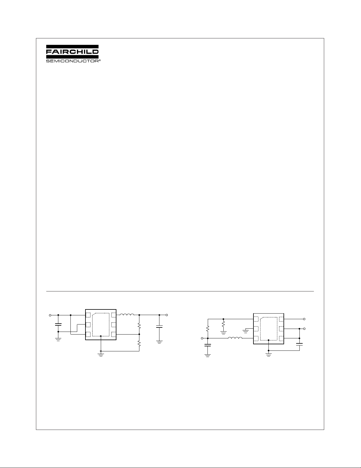
Typical Application
V
IN
C
IN
10µF
FAN2001/FAN2002 Rev. 1.0.2
©2005 Fairchild Semiconductor Corporation
PGND
EN
1
P1
2
GND)
(A
3
FAN2001
SW
6
3.3µH
5
NC
FB
4
R1
R2
5KΩ
10KΩ
V
OUT
1.2V (1A)
C
OUT
2 x 10µF
V
OUT
1.2V (1A)
R1
R2
5K
Ω
2 x 10µF
10K
Ω
L1
3.3µH
FB
PGND
SW
1
P1
2
(A
GND)
3
EN
6
V
IN
5
PV
IN
4
10µF
FAN2002
Figure 1. Typical Application
1
www.fairchildsemi.com
Page 2
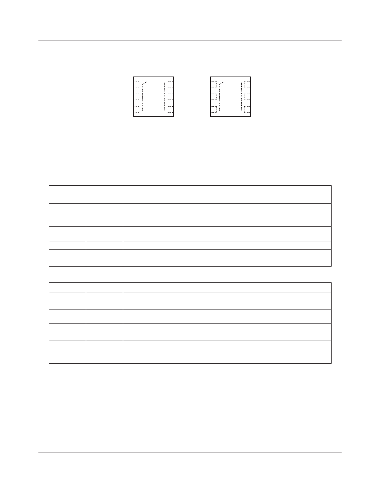
Pin Assignment
FAN2001/FAN2002 1A High-Efficiency Step-Down DC-DC Converter
Top View
V
1
IN
P1
PGND
2
(AGND)
3
EN FB
SW
6
5
NC
4
FB
1
P1
PGND
2
(AGND)
3
SW PV
EN
6
5
V
IN
4
IN
FAN2001 FAN2002
3x3mm 6-Lead MLP
Figure 2. Pin Assignment
Pin Description
FAN2001 (3x3mm 6-Lead MLP)
Pin No. Pin Name Pin Description
P1 AGND Analog Ground. P1 must be soldered to the PCB ground.
1V
2 PGND Power Ground. This pin is connected to the internal MOSFET switches. This pin must be
3ENEnable Input. Logic high enables the chip and logic low disables the chip, reducing the supply
4 FB Feedback Input. Adjustable voltage option, connect this pin to the resistor divider.
5NCNo Connection Pin.
6SWSwitching Node. This pin is connected to the internal MOSFET switches.
IN
Supply Voltage Input.
externally connected to AGND.
current to less than 1µA. Do not float this pin.
FAN2002 (3x3mm 6-Lead MLP)
Pin No. Pin Name Pin Description
P1 AGND Analog Ground. P1 must be soldered to the PCB ground.
1FBFeedback Input. Adjustable voltage option, connect this pin to the resistor divider.
2 PGND Power Ground. This pin is connected to the internal MOSFET switches. This pin must be exter-
3SWSwitching Node. This pin is connected to the internal MOSFET switches.
4 PV
5V
6ENEnable Input. Logic high enables the chip and logic low disables the chip, reducing the supply
IN
nally connected to AGND.
Supply Voltage Input. This pin is connected to the internal MOSFET switches.
IN
Supply Voltage Input.
current to less than 1µA. Do not float this pin.
FAN2001/FAN2002 Rev. 1.0.2
2
www.fairchildsemi.com
Page 3

(
µ
FAN2001/FAN2002 1A High-Efficiency Step-Down DC-DC Converter
Absolute Maximum Ratings
(Note1)
Parameter Min Max Unit
V
, PV
IN
IN
Voltage On Any Other Pin -0.3 V
Lead Soldering Temperature (10 seconds) 260 °C
Junction Temperature 150 °C
Storage Temperature -65 150 °C
Thermal Resistance-Junction to Tab
Electrostatic Discharge Protection (ESD) Level (Note 3) HBM 4 kV
,
θ
)
3x3mm 6-lead MLP (Note 2)
JC
CDM 1
-0.3 7 V
IN
8 °C/W
V
Recommended Operating Conditions
Parameter Min Typ Max Unit
Supply Voltage Range 2.5 5.5 V
Output Voltage Range, Adjustable Version 0.8 V
Output Current 1A
Inductor (Note 4) 3.3
Input Capacitor (Note 4) 10 µF
Output Capacitor (Note 4) 2 x 10 µF
Operating Ambient Temperature Range -40 +85 °C
Operating Junction Temperature Range -40 +125 °C
IN
V
H
Notes:
1. Stresses above those listed under “Absolute Maximum Ratings” may cause permanent damage to the device. This is a stress rating only and functional
operation of the device at these or any other conditions above those indicated in the operational section of this specification is not implied. Exposure
to absolute maximum rating conditions for extended periods may affect device reliability. Absolute maximum ratings apply individually only, not in
combination. Unless otherwise specified, all other voltages are referenced to AGND.
2. Junction to ambient thermal resistance, θ
via used, diameter of via used, available copper surface, and attached heat sink characteristics.
3. Using Mil Std. 883E, method 3015.7(Human Body Model) and EIA/JESD22C101-A (Charge Device Model).
4. Refer to the applications section for further details.
, is a strong function of PCB material, board thickness, thickness and number of copper planes, number of
JA
FAN2001/FAN2002 Rev. 1.0.2
3
www.fairchildsemi.com
Page 4
≤
≤
Electrical Characteristics
V
= V
IN
Unless otherwise noted. Typical values are at T
Symbol Parameter Conditions Min. Typ. Max. Units
V
IN
I
Q
V
ENH
V
ENL
I
EN
R
DS-ON
I
LIM
I
lkg_(N)
I
lkg_(P)
Vref Reference Voltage 0.8 V
Notes:
5. Refer to the application section for further details.
6. For output voltages ≤ 1.2V a 40 µ F output capacitor value is required to achieve a maximum output accuracy of 3% while operating in power save
mode (PFM mode).
+ 0.6V(min. 2.5V) to 5.5V, I
OUT
Input Voltage 0 mA ≤ I
0 mA ≤ I
Quiescent Current I
OUT
I
OUT
switching (Note 5)
= 350mA, V
OUT
= 25°C.
A
600 mA 2.5 5.5 V
OUT
1000 mA 2.7 5.5 V
OUT
=1.2V, EN = V
OUT
, T
= -40°C to +85°C,
IN
A
= 0mA, Device is not switching 20 35
= 0mA, Device is
R2 =10K Ω
R2 =100K Ω
50
25
Shutdown Supply Current EN = GND 0.1 1
Undervoltage Lockout
Threshold
V
Rising 1.9 2.1 2.3 V
IN
Hysteresis 150 mV
Enable High Input Voltage 1.3 V
Enable Low Input Voltage 0.4 V
EN input bias current EN = V
PMOS On Resistance V
V
NMOS On Resistance V
V
P-channel current limit 2.5V < V
or GND 0.01 0.1
IN
= V
= 5.5V 250 350 m Ω
IN
GS
= V
= 2.5V 300 400
IN
GS
= V
= 5.5V 200 300 m Ω
IN
GS
= V
= 2.5V 250 350
IN
GS
< 5.5V 1300 1500 2000 mA
IN
Oscillator frequency 1000 1300 1500 KHz
N-channel leakage current V
P-channel leakage current V
Line regulation I
Load regulation 350 mA ≤ I
Output DC Voltage Accuracy
(Note 6)
Over-Temperature Protection PWM Mode Only
= 5.5V 0.1 1
DS
= 5.5V 0.1 1
DS
10 mA 0.16 %/V
OUT
1000 mA 0.15 %
OUT
0 mA ≤ I
350 mA ≤ I
1000 mA -3 +3 %
OUT
OUT
1000 mA
Rising
Temperature
150 °C
Hysteresis 20 °C
Start-Up Time I
= 1000 mA, C
OUT
= 20 µF 800 µS
OUT
µ
A
µ
A
µ
A
µ
A
µ
A
µ
A
µ
A
≤
≤
≤
≤
FAN2001/FAN2002 1A High-Efficiency Step-Down DC-DC Converter
FAN2001/FAN2002 Rev. 1.0.2
4
www.fairchildsemi.com
Page 5
Typical Performance Characteristics
T
= 25°C, C
A
100
95
90
85
80
75
Efficiency (%)
70
65
60
1101001000
= 10µF, C
IN
= 20µF, L = 3.3µH, R2 = 10KΩ, unless otherwise noted.
OUT
Efficiency vs. Load Current Efficiency vs. Load Current
VIN = 5V
V
VIN = 3.6 V
V
= 3V
OUT
= 3.3V
OUT
VIN = 3.6V
V
= 1.2V
OUT
Load Current (mA) Load Current (mA)
100
95
90
85
80
75
70
65
60
VIN = 5.5V
55
Efficiency (%)
50
45
40
35
0.1 1 10 100 1000
VIN = 3.9V
V
= 3.3V
OUT
R2 = 100KΩ
FAN2001/FAN2002 1A High-Efficiency Step-Down DC-DC Converter
Efficiency vs. Load Current
100
V
= 1.2V
OUT
90
R2 = 100KΩ
80
70
60
50
Efficiency (%)
VIN = 3.6 V
40
30
0.1 1 10 100 1000
VIN = 2.5V
VIN = 5.5V
Load Current (mA) Load Current (mA)
Quiescent Current vs. Input Voltage
80
V
= 1.2 V
OUT
70
60
50
40
R2 = 10KΩ
30
20
Quiescent Current (µA)
10
0
2.5 3.0 3.5 4.0 4.5 5.0 5.5
Input Voltage (V)
R2 = 100KΩ
Output Voltage vs. Load Current
1.214
1.212
1.210
1.208
1.206
1.204
1.202
1.200
1.198
Output Voltage (V)
1.196
1.194
1.192
VIN = 5V
0200 400 600 800 1000
Frequency vs. Temperature
1400
1380
1360
1340
1320
1300
1280
1260
1240
Oscillator Frequency (kHz)
1220
1200
-40 -20 0 20 40 60 80 100
VIN = 5.5V
VIN = 3.6V
VIN = 2.5V
Temperature (°C)
FAN2001/FAN2002 Rev. 1.0.2
5
www.fairchildsemi.com
Page 6
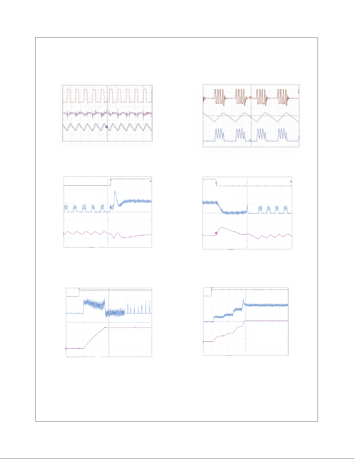
Typical Performance Characteristics (Contd.)
TA = 25°C, CIN = 10µF, C
PWM Mode Power Save Mode
Vol tage
(2V/div)
SW Node
Output
Vol tage
(5mV/div)
Inductor
Current
(200mA/div)
= 20µF, L = 3.3µH, R2 = 10KΩ, unless otherwise noted.
OUT
Time (1µs/div)
Vol tage
SW Node
Output
Vol tage
(20mV/div)
Inductor
Current
FAN2001/FAN2002 1A High-Efficiency Step-Down DC-DC Converter
(2V/div)
(200mA/div)
Time (5µs/div)
Load Current
Inductor
Output
Vol tag e at
Inductor
Output
Step
Current
(500mA/div)
Vol tag e
(50mV/div)
(5V/Div)
Enable Pin
Current
(200mA/div)
Vol tag e
(500mV/div)
Load Transient Response
100mA
V
= 1.2V
OUT
Time (10µs/div)
Start-Up Response
V
OUT
I
OUT
Time (100µs/div)
600mA
= 1.2V
= 10mA
Step
Load Current
Inductor
Current
Output
Vol tage
(5V/Div)
Vol tag e at
Enable Pin
Inductor
Current
Output
Vol tage
Load Transient Response
600mA
V
= 1.2V
OUT
(500mA/div)
(50mV/div)
Time (10µs/div)
Start-Up Response
(500mA/div)
(500mV/div)
Time (20 0µs/div)
100mA
V
I
OUT
OUT
= 1.2V
= 1000mA
FAN2001/FAN2002 Rev. 1.0.2
6 www.fairchildsemi.com
Page 7
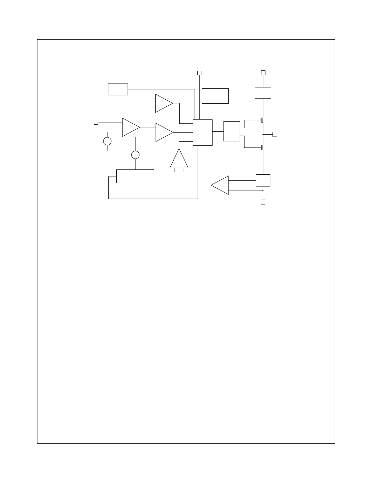
Block Diagram
FB
DIGITAL
SOFT START
0.8V
ERROR
AMP
IS
REF
PFM
COMP
COMP
EN
UNDER-VOLTAGE
LOCKOUT
LOGIC
CONTROL
MOSFET
DRIVER
IS
V
IN
CURRENT
SENSE
FAN2001/FAN2002 1A High-Efficiency Step-Down DC-DC Converter
SW
GND
IS
OSC
SLOPE COMPENSATION
OVER
VOLTAGE
COMP
REF FB
Figure 3. Block Diagram
Detailed Operation Description
The FAN2001/FAN2002 is a step-down converter operating in a
current-mode PFM/PWM architecture with a typical switching
frequency of 1.3MHz. At moderate to heavy loads, the converter
operates in pulse-width-modulation (PWM) mode. At light loads
the converter enters a power-save mode (PFM pulse skipping)
to keep the efficiency high.
PWM Mode
In PWM mode, the device operates at a fixed frequency of
1.3MHz. At the beginning of each clock cycle, the P-channel
transistor is turned on. The inductor current ramps up and is
monitored via an internal circuit. The P-channel switch is turned
off when the sensed current causes the PWM comparator to trip
when the output voltage is in regulation or when the inductor
current reaches the current limit (set internally to typically
1500mA). After a minimum dead time the N-channel transistor
is turned on and the inductor current ramps down. As the clock
cycle is completed, the N-channel switch is turned off and the
next clock cycle starts.
PFM (Power Save) Mode
As the load current decreases and the inductor current reaches
negative value, the converter enters pulse-frequency-modulation (PFM) mode. The transition point for the PFM mode is given
by the equation:
1V
I
OUTVOUT
------------------------------------------
×=
The typical output current when the device enters PFM mode is
150mA for input voltage of 3.6V and output voltage of 1.2V. In
OUTVIN
2Lf××
⁄()–
NEG.
NEG.
LIMIT
COMP
LIMIT
SENSE
GND
PFM mode the device operates with a variable frequency and
constant peak current, thus reducing the quiescent current to
minimum. Consequently, the high efficiency is maintained at
light loads. As soon as the output voltage falls below a threshold, set at 0.8% above the nominal value, the P-channel transistor is turned on and the inductor current ramps up. The Pchannel switch turns off and the N-channel turns on as the peak
inductor current is reached (typical 450mA).
The N-channel transistor is turned off before the inductor current becomes negative. At this time the P-channel is switched
on again starting the next pulse. The converter continues these
pulses until the high threshold (typical 1.6% above nominal
value) is reached. A higher output voltage in PFM mode gives
additional headroom for the voltage drop during a load transient
from light to full load. The voltage overshoot during this load
transient is also minimized due to active regulation during turn
on of the N-channel rectifier switch. The device stays in sleep
mode until the output voltage falls below the low threshold. The
FAN2001/FAN2002 enters the PWM mode as soon as the output voltage can no longer be regulated in PFM with constant
peak current.
100% Duty Cycle Operation
As the input voltage approaches the output voltage and the duty
cycle exceeds the typical 95%, the converter turns the P-channel transistor continuously on. In this mode the output voltage is
equal to the input voltage minus the voltage drop across the Pchannel transistor:
V
= VIN – I
OUT
R
= P-channel switch ON resistance
dsON
I
= Output current
LOAD
RL = Inductor DC resistance
LOAD
× (R
+ RL), where
dsON
FAN2001/FAN2002 Rev. 1.0.2
7 www.fairchildsemi.com
Page 8
FAN2001/FAN2002 1A High-Efficiency Step-Down DC-DC Converter
UVLO and Soft Start
The reference and the circuit remain reset until the VIN crosses
its UVLO threshold.
The FAN2001/FAN2002 has an internal soft-start circuit that
limits the in-rush current during start-up. This prevents possible
voltage drops of the input voltage and eliminates the output voltage overshoot. The soft-start is implemented as a digital circuit
increasing the switch current in four steps to the P-channel current limit (1500mA). Typical start-up time for a 20µF output
capacitor and a load current of 1000mA is 800µs.
Short Circuit Protection
The switch peak current is limited cycle-by-cycle to a typical
value of 1500mA. In the event of an output voltage short circuit,
the device operates with a frequency of 400kHz and minimum
duty cycle, therefore the average input current is typically
200mA.
Thermal Shutdown
When the die temperature exceeds 150°C, a reset occurs and
will remain in effect until the die cools to 130°C, at that time the
circuit will be allowed to restart.
Applications Information
Setting the Output Voltage
The internal reference is 0.8V (Typical). The output voltage is
divided by a resistor divider, R1 and R2 to the FB pin. The output voltage is given by:
R
1
=
SW
6
5
NC
FB
4
1
-------+
R
2
3.3µH
C
50KΩ
R1
100KΩ
R2
V
OUT
f
1.2V (1A)
C
OUT
2 x 10µF
V
OUTVREF
Where R
+ R2 < 800KΩ.
1
According to this equation, and assuming desired output voltage of 1.5096V, and given R2 = 10KΩ, the calculated value of
R1 is 8.87KΩ. If quiescent current is a key design parameter a
higher value feedback resistor can be used (e.g. R2 = 100KΩ)
and a small bypass capacitor of 10pF is required in parallel with
the upper resistor as shown in Figure 4.
V
IN
10µF
C
IN
PGND
1
P1
2
(AGND)
EN
3
This is calculated as follows:
∆ILV
1V
×=
-----------------------------------------
OUT
⁄()–
OUTVIN
Lf×
where:
∆IL = Inductor Ripple Current
f = Switching Frequency
L = Inductor Value
Some recommended inductors are suggested in the table
below:
Inductor Value Vendor Part Number
3.3µH Panasonic ELL6PM3R3N
3.3µH Murata LQS66C3R3M04
Table 1: Recommended Inductors
Capacitors Selection
For best performances, a low ESR input capacitor is required. A
ceramic capacitor of at least 10µF, placed as close to the V
and AGND pins of the device is recommended. The output
capacitor determines the output ripple and the transient
response.
Capacitor
Vendor Part Number
Value
10µF Taiyo Yuden JMK212BJ106MG
JMK316BJ106KL
TDK C2012X5ROJ106K
C3216X5ROJ106M
Murata GRM32ER61C106K
Table 2: Recommended Capacitors
PCB Layout Recommendations
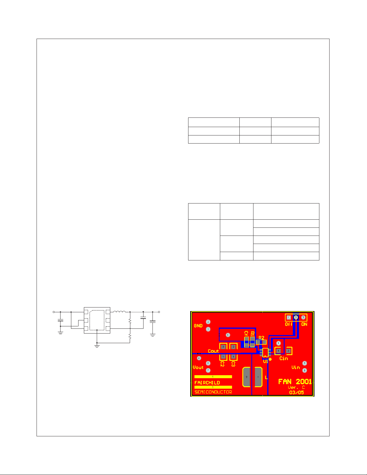
The recommended PCB layout is shown in Figures 5 and 6. The
inherently high peak currents and switching frequency of power
supplies require a careful PCB layout design.
IN
Figure 4. Setting the Output Voltage
Inductor Selection
The inductor parameters directly related to the device’s performances are saturation current and dc resistance. The FAN2001/
FAN2002 operates with a typical inductor value of 3.3µH. The
lower the dc resistance, the higher the efficiency. For saturation
current, the inductor should be rated higher than the maximum
load current plus half of the inductor ripple current.
FAN2001/FAN2002 Rev. 1.0.2
Figure 5. Recommended PCB Layout (FAN2001)
8 www.fairchildsemi.com
Page 9
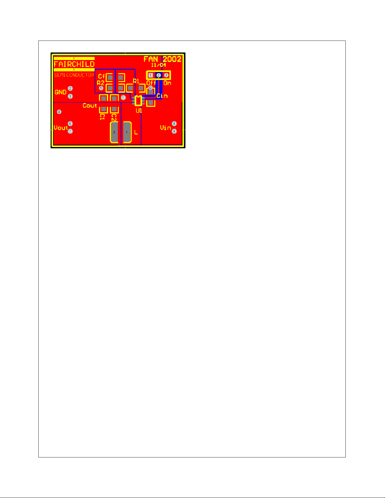
Figure 6. Recommended PCB Layout (FAN2002)
FAN2001/FAN2002 1A High-Efficiency Step-Down DC-DC Converter
Therefore, use wide traces for high current paths and place the
input capacitor, the inductor, and the output capacitor as close
as possible to the integrated circuit terminals. In order to minimize voltage stress to the device resulting from ever present
switching spikes, use an input bypass capacitor with low ESR.
Note that the peak amplitude of the switching spikes depends
upon the load current; the higher the load current, the higher the
switching spikes. The resistor divider that sets the output voltage should be routed away from the inductor to avoid RF coupling. The ground plane at the bottom side of the PCB acts as
an electromagnetic shield to reduce EMI.
For more board layout recommendations download the application note “PCB Grounding System and FAN2001/FAN2011 High
Performance DC-DC Converters” (AN-42036).
FAN2001/FAN2002 Rev. 1.0.2
9 www.fairchildsemi.com
Page 10
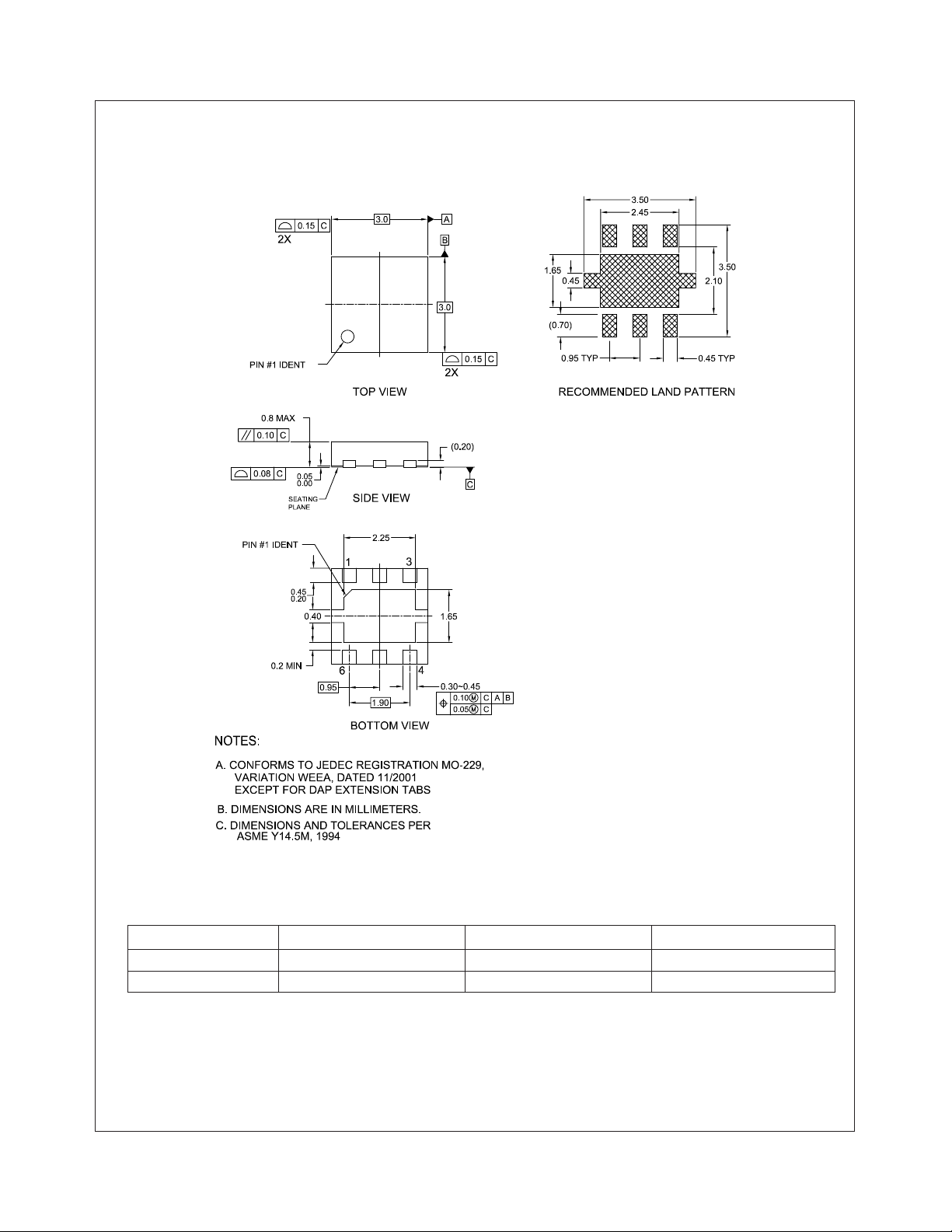
Mechanical Dimensions
3x3mm 6-Lead MLP
FAN2001/FAN2002 1A High-Efficiency Step-Down DC-DC Converter
Ordering Information
Product Number Output Voltage Package Type Order Code
FAN2001 Adjustable 3x3mm 6-Lead MLP FAN2001MPX
FAN2002 Adjustable 3x3mm 6-Lead MLP FAN2002MPX
FAN2001/FAN2002 Rev. 1.0.2
10 www.fairchildsemi.com
Page 11

TRADEMARKS
The following are registered and unregistered trademarks Fairchild Semiconductor owns or is authorized to use and is
not intended to be an exhaustive list of all such trademarks.
ACEx™
ActiveArray™
Bottomless™
FPS™
CoolFET™
CROSSVOL T™
DOME™
EcoSPARK™
2
CMOS™
E
EnSigna™
FACT™
FACT Quiet Series™
Across the board. Around the world.™
The Power Franchise
Programmable Active Droop™
DISCLAIMER
FAIRCHILD SEMICONDUCTOR RESERVES THE RIGHT TO MAKE CHANGES WITHOUT FURTHER NOTICE TO ANY
PRODUCTS HEREIN TO IMPROVE RELIABILITY, FUNCTION OR DESIGN. FAIRCHILD DOES NOT ASSUME ANY LIABILITY
ARISING OUT OF THE APPLICATION OR USE OF ANY PRODUCT OR CIRCUIT DESCRIBED HEREIN; NEITHER DOES IT
CONVEY ANY LICENSE UNDER ITS PATENT RIGHTS, NOR THE RIGHTS OF OTHERS.
LIFE SUPPORT POLICY
FAST
FASTr™
LittleFET™
FRFET™
GlobalOptoisolator™
GTO™
HiSeC™
2
C™
I
i-Lo™
ImpliedDisconnect™
IntelliMAX™
ISOPLANAR™
MICROCOUPLER™
MicroFET™
MicroPak™
MICROWIRE™
MSX™
MSXPro™
OCX™
OCXPro™
OPTOLOGIC
OPTOPLANAR™
PACMAN™
POP™
Power247™
PowerEdge™
PowerSaver™
PowerTrench
QFET
QS™
QT Optoelectronics™
Quiet Series™
RapidConfigure™
RapidConnect™
µSerDes™
SILENT SWITCHER
SMART START™
SPM™
Stealth™
SuperFET™
SuperSOT™-3
SuperSOT™-6
SuperSOT™-8
SyncFET™
TinyLogic
TINYOPTO™
TruTranslation™
UHC™
UltraFET
UniFET™
VCX™
FAN2001/FAN2002 1A High-Efficiency Step-Down DC-DC Converter
FAIRCHILD’S PRODUCTS ARE NOT AUTHORIZED FOR USE AS CRITICAL COMPONENTS IN LIFE SUPPORT
DEVICES OR SYSTEMS WITHOUT THE EXPRESS WRITTEN APPROVAL OF FAIRCHILD SEMICONDUCTOR CORPORATION.
As used herein:
1. Life support devices or systems are devices or
systems which, (a) are intended for surgical implant into
the body, or (b) support or sustain life, or (c) whose
failure to perform when properly used in accordance
with instructions for use provided in the labeling, can be
reasonably expected to result in significant injury to the
user.
PRODUCT STATUS DEFINITIONS
Definition of Terms
Datasheet Identification Product Status Definition
Advance Information
Preliminary
No Identification Needed
Formative or
In Design
First Production
Full Production
2. A critical component is any component of a life
support device or system whose failure to perform can
be reasonably expected to cause the failure of the life
support device or system, or to affect its safety or
effectiveness.
This datasheet contains the design specifications for
product development. Specifications may change in
any manner without notice.
This datasheet contains preliminary data, and
supplementary data will be published at a later date.
Fairchild Semiconductor reserves the right to make
changes at any time without notice in order to improve
design.
This datasheet contains final specifications. Fairchild
Semiconductor reserves the right to make changes at
any time without notice in order to improve design.
Obsolete
FAN2001/FAN2002 Rev. 1.0.2
Not In Production
This datasheet contains specifications on a product
that has been discontinued by Fairchild semiconductor.
The datasheet is printed for reference information only.
Rev. I15
11 www.fairchildsemi.com
 Loading...