

Page 1
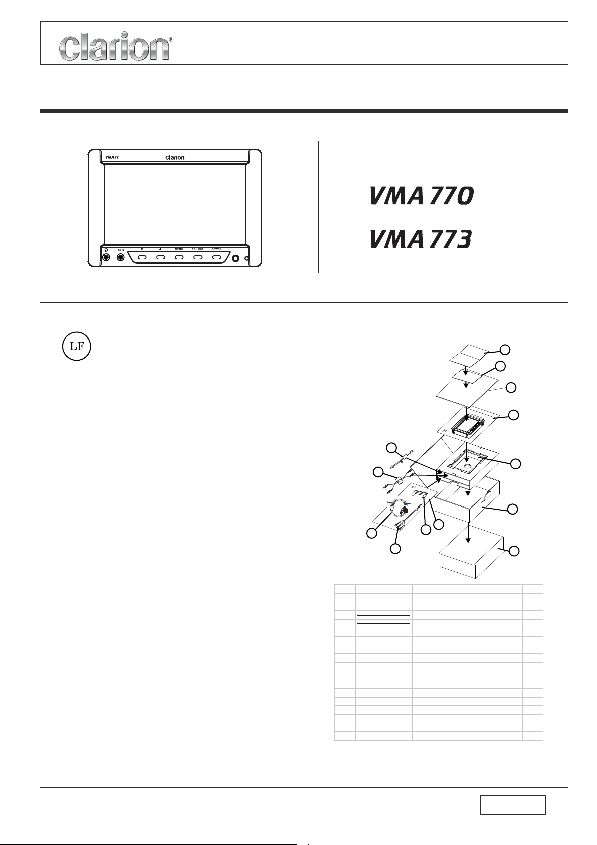
REF PART No. DESCRIPTION Q'TY
1 MA2A-704002-1R User’s Manual (VMA770) 1
1 MA2A-704003-1R User’s Manual (VMA773) 1
2 Warranty card USA (VMA770) 1
2 Warranty card EUROPE(VMA773) 1
3 PA2B612002-1R E PEspacer 1
4 PA2P701002-1R P Ebag 180*270*0.5 mm 1
5 BX20612002-1R Inner corrugated box 1
6 CL-4216-02-1R P OWERFILTER 1
7 CL-2292-01-1R AUDIO FILTER 1
8 CL-8872-01-1R RCA AV CABLE 1
9 CL-1312-01-1R RCA cable 1
10 PA2B612005-1R METAL IN SERT CARD(VM A773) 1
10 PA2B707005-1R PLATICINSERTCARD(VMA770) 1
11 PA2B707005-1R PEbag 163*342*0.2 mm 1
12 BX20612001-1R Inner white box 1
13 BX20705005-1R Gift box (VMA770) 1
13 BX20705004-1R Gift box (VMA773) 1
Reedition: 2008.01.29
Clarion Co., Ltd.
7-2,Shintoshin, Chuo-ku, Saitama-shi,Saitama 330-0081 Japan
ServiceDept.: 7-2,Shintoshin, Chuo-ku,Saitama-shi,Saitama 330-0081Japan
Tel:+81-48-601-3705 FAX:+81-48-601-3804
Published by Service Dept.
298-6491-00
Printed in Taiwan R.O.C
Jan.2008
Service Manual
0
7” Wide Screen Color LCD Monitor
Model
(ZM-5003B-A)
Model
(ZM-5002E-A)
This product is a lead free model.
Lead free solder is used in PWB stamped LF mark.
Please keep the following conditions when you repair.
1. Use lead free solder.
2. Use a nitrogen solder system.
3. Do not use "General solder" and "lead free
solder" together.
SPECIFICATIONS
Display Unit
Display type: Color TFT Active Matrix
LCD Screen size: 7”
Pixels: 480 RGB (H) x 234 (V)
Screen resolution: 336,960 dots
Video input lever(RCA):
1.0 volts peak to peak
Video format: NTSC, PAL
Power requirement: 12V DC (10.8V-15.6V)
Power consumption: 7 watts,power on - typical0.6amps
(600mA) - typical
Dimensions(mm): 192.7(W)x133.5(H)x32.5(D)(with
Bezel)
Weight: 400g
COMPONENTS
6
TER
DCFIL
GND
+12V
7
04
-
8
10
9
11
1
2
3
4
04
-
5
12
13
NOTES
* The technical dataand the design ofthe equipment may
change for the sake of technical improvement without
prior notice.
-1-
VMA770
VMA773
Page 2
Toengineersinchargeof
Repair or Inspection of our
products:
Before repair orinspection, make sureto
follow the instructionsso that customersand
Engineers in chargeof repair orinspection
can avoid sufferingAny riskorinjury.
1. Use specified parts.
The system uses partswithspecialsafetyfeatures
against Fire and voltage.Useonlypartswithequivalent
characteristics when replacing hem. The use of
unspecified parts shall beregardedasremodelingfor
which we shall notbeliable. The onus of product
liability (PL) shall notbeourresponsibilityincases
where an accident orfailureisasaresultofunspecified
parts being used.
2. Place the partsandwiringbackintheiroriginal
positions after replacement orre-wiring.
For proper circuit construction,useofinsulationtubes,
bonding, gaps to PWB,etc,isinvolved.Thewiring
connection and routing tothePWBarespecially
planned using clamps tokeepawayfromheatedand
high voltage parts. Ensurethattheyareplacedbackin
their original positions afterrepairorinspection.
If extended damage iscausedduetonegligenceduring
repair, the legal responsibilityshallbewiththerepairing
company.
3. Check for safetyafterrepair.
Check that the screws,partsandwiresareputback
securely in their originalpositionafterrepair.Ensurefor
safety reasons there isnopossibilityofsecondary
p oblems around therepairedspots. If extended
r
damage is caused duetonegligenceofrepair,thelegal
responsibility shall be withtherepairingcompany.
4. Caution in removalandmakingwiringconnectiontothe
parts for the automobile.
Disconnect the battery terminalafterturningtheignition
key off. If wrongwiringconnectionsaremadewiththe
battery connected, a shortcircuitand/orfiremayoccur.
If extensive damage iscausedduetonegligenceof
repair, the legal responsibilityshallbewiththerepairing
company.
5. Cautions in soldering
Please do not spreadliquidfluxinsoldering.
Please do not washthesolderingpointaftersoldering.
6. Cautions in solderingforchipcapacitors
Please solder the chipcapacitorsafterpre-heatingfor
replacement because they areveryweaktoheat.
Please do not heatthechipcapacitorswithasoldering
iron
directly.
7. Cautions in handlingforchipparts.
Do not reuse removedchipsevenwhennoabnormality
is observed in theirappearance.Alwaysreplacethem
with new ones. (Thechippartsincluderesistors,
capacitors, diodes, transistors,etc).
Please make an operationtestafterreplacement.
8. Cautions in handlingflexiblePWB
Before working with asolderingiron,makesurethatthe
iron tip temperature isaround270.Takecarenotto
apply the iron tiprepeatedly(morethanthreetimes)to
the same patterns. Also
take care not toapplythetipwithforce.
9. Turn the unitOFFduringdisassemblyandparts
replacement.
Recheck all work beforeyouapplypowertotheunit.
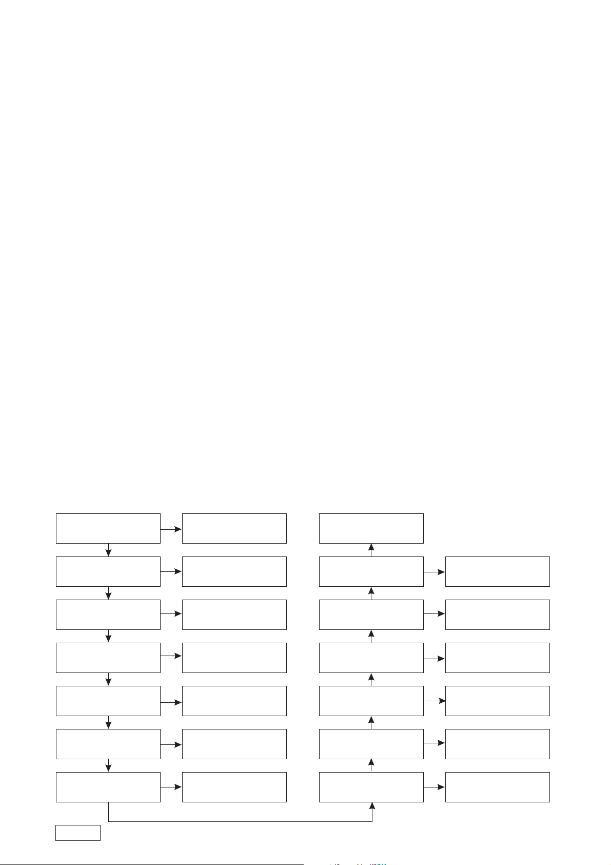
TROUBLESHOOTING
1. The image is unusual & No image
Normal signal is
obtained at each
terminal of J1?
YES YES
Circuit current flows
normally?
YES YES
Av1 video signal is
obtained at L12?
YES YES
Av2 video signal is
obtained at L9?
YES YES
VCC3(3.3V) is obtained
at Pin-2 of U16?
YES YES
AVCC3(3.3V) is
obtained at Pin-2 of
U18?
YES YES
VCC18(1.8V) is
obtained at Pin-2 of
U19?
Check the J1, Input
connection flexible
NO
cables and its
Go to item (3)NoPower
NO
Check the J1, Input
connection flexible
NO NO
cables and its
Check the J3 andJ7
Input connection
NO
flexible cables and their
Go to item (3)NoPower
NO
Go to item (3)NoPower
NO NO
Go to item (3)NoPower
NO
Replace LCD panel
Normal signal is
obtained at each
terminal of J4?
Panel-VCC(5V) is
obtained at L22?
VCC12V is obtained at
L30?
RGB signal for LCDis
obtained at Pin-22 to
Pin-24 of J4?
Normal Vcom signal is
obtained at Tp3?
Check the Y2 at27
Mhz?
Check the J4, Input
connection flexible
NO
cables and its
Go to item (3)NoPower
Go to item (3)NoPower
NO
Check the Q6 toQ8and
its periphery.
NO
Check the L32 andits
periphery.
Check the Y2 andits
periphery.
NO
VMA770
VMA773
YES
- 2-
Page 3
2. No sound
AV1 Audio-L signal is
obtained at L3?
YES YES
AV1 Audio-R signal is
obtained at L4?
YES YES
AV2 Audio-L signal is
obtained at L7?
YES YES
AV2 Audio R signal is
obtained at L8?
Audio L signal is
obtained at C93?
-
YES YES
END
Check the J1, Input
connection flexible
NO
cables and its
Check the J1, Input
connection flexible
NO NO
cables and its
Check the J3 andJ7
Input connection
NO
flexible cables and their
Check the J3 andJ7
Input connection
flexible cables and their
NO
Check the U11 andtheir
periphery.
NO
IR_Aurio-R signal are
YES
obtained at Pin-1 &Pin-
Check the TP2 at3.8
Mhz of IR_CHB_AudioR?
Check the TP1 at3.2
Mhz of IR_CHB_AudioL?
Check the TP2 at2.8
Mhz of IR_CHA_AudioR?
Check the TP1 at2.3
Mhz of IR_CHA_AudioL?
VA5_IR is obtained at
L26?
NO
YES
NO
NO
NO
NO
IR_Audio-R and
Check U13, U14 and
their periphery.
Check U12, U14 and
their periphery.
Check U12, U14 and
their periphery.
Check U12, U14 and
their periphery.
Check U12, U14 and
their periphery.
Go to item (3)NoPower
YES
Audio R signal is
obtained at C89?
YES
VA5 is obtained atL23?
3. No Power
F1(fuse) is broken out?
YES YES
DC12V is obtained at
L1?
YES YES
VCC12 is obtained at
L27
YES YES
YES
Check the U8 andtheir
periphery.
NO
Go to item (3)NoPower
NO
YES
Replace F1.
NO
Check the F1, input
flexible cables and their
NO
periphery.
Check Q1, Q2 andtheir
periphery.
NO NO
Audio_R OUT signal is
obtained at L5?
YES
Audio_L OUT signal is
obtained at L6?
END
VCC12V is obtained at
L25 (For IR_LED)?
VCC12V is obtained at
L30 (For U17 Inverter
control IC)?
NO
NO
NO
Check the U9, U10,J3,
J6 Input connectiog
flexible cables and their
Check the U9, U10,J3,
J6 Input connectiog
flexible cables and their
Check Q20, Q21, Q23
and their periphery.
Check Q10, Q11, Q12
and their periphery.
5VSTB is obtained at
L29?
YES YES
VCC5 is obtained at
L28?
YES YES
VCC3(3.3V) is obtained
at Pin-2 of U16?
YES YES
AVCC3(3.3V) is
obtained at Pin-2 of
U18?
Check U15, Q15, Q16
NO
and their periphery.
Check Q17, Q18, Q19
and their periphery.
NO
Check U16 and their
periphery.
NO NO
Check U18 and their
periphery.
NO
YES
VA5_IR is obtained at
L26?
VA5 is obtained atL23?
PANEL-VCC is
obtained at L22?
VCC18(1.8V) is
obtained at Pin-2 of
U19?
NO
NO
NO
- 3-
Check L26 and their
periphery.
Check L23 and their
periphery.
Check Q3, Q4, Q5and
their periphery.
Check the U19 andtheir
periphery.
VMA770
VMA773
Page 4
EXPLANATION OF IC
Pin# NAME DESCRIPTION
1 OUT Open collector transistor output
2 VCC IC power supply
3 COMP Error Amplifier feedback output
4 FB error amplifier inverting input
5 SCP short circuit protection input
6 DTC dead-time control input
7 RT A resistance of Oscillator
8 GND IC Ground
Pin# NAME DESCRIPTION
1 IA0 DATA INPUTS
2 IA1 DATA INPUTS
3 IA2 DATA INPUTS
4 GND GROUND
5 YA DATA INPUTS
6 S0 SELECT INPUT
7 S1 SELECT INPUT
8VCCPOWER
Pin# NAME DESCRIPTION
1 Vcc1 Power supply
2 Modu1 FM. Modulation in
3 Fadj1 Frequency adjust
4Vss1GND
5 Modu2 FM. Modulation in
6 Fadj2 Frequency adjust
7Vss2GND
8 Fo2 Frequency out
9 Tc Off timecontrol
10 Tr2 Trigger on
11 Vcc2 Power supply
12 Fo1 Frequency out
13 No
14 Tr1 Trigger on
Pin# NAME DESCRIPTION
1 P4.2 Bit2 of port 4
2 P1.0/T2 Bit0 of port 1& timer 2 clock out
3 P1.1/T2EX Bit1 of port 1& timer 2 control
4 P1.2 Bit2 of port 1
5 P1.3 Bit3 of port1& SPWM channel 0
6 P1.4 Bit4 of port1& SPWM channel 1
7 P1.5 Bit5 of port1& SPWM channel 2
8 P1.6 Bit6 of port1& SPWM channel 3
9 P1.7 Bit7 of port1& SPWM channel 4
10 RST REST
11 P3.0/RXD Bit0 of port3& Receiver data
12 P4.0 Bit0 of port 4
12 P4.3 Bit3 of port 4
13 P4.3/INT2 Bit1 of port3& Transmit data
14 P3.1/INT0 Bit 2 of port 3&low true interrupt 0
15 P3.3/INT1 Bit 3 of port 3&low true interrupt 1
16 P3.4/T0 Bit4 of port 3 & Timer 0
17 P3.5/T1 Bit5 of port 3 & Timer 1
18 P3.5/T1P3.6/WR Bit6 of port 3 & ext. memory write
19 P3.7/RD Bit7 of port 3& ext. memory read
20 XTAL2 Crystal out
21 XTAL1 Crystal in
22 GND Sink Voltage, Ground
24 P2.0/A8 Bit0 of port 2 & bit8 of ext.memory add.
25 P2.1/A9 Bit1 of port 2 & bit9 of ext.memory add.
26 P2.2/A1.0 Bit2 of port 2 & bit10 of ext.memory add.
27 P2.3/A11 Bit3 of port 2 & bit11 of ext.memory add.
28 P2.4/A12 Bit4 of port 2 & bit12 of ext.memory add.
29 A13/P2.5 Bit5 of port 2 & bit13 of ext.memory add.
30 A14/P2.6 Bit6 of port 2 & bit14 of ext.memory add.
31 A15/P2.7 Bit7 of port 2 & bit15 of ext.memory add.
32 PSEN Progr a mstorag eenable
33 ALE add. latch enable
34 P4.1 Bit1 of port 4
35 EA External access
36 AD7/P0.7 Bit7 of port 0 & data/add. bit 7of ext. memory
37 AD6/P0.6 Bit6 of port 0 & data/add. bit 6of ext. memory
38 AD5/P0.5 Bit5 of port 0 & data/add. bit 5of ext. memory
39 AD4/P0.4 Bit4 of port 0 & data/add. bit 4of ext. memory
40 AD3/P0.3 Bit3 of port 0 & data/add. bit 3of ext. memory
41 AD2/P0.2 Bit2 of port 0 & data/add. bit 2of ext. memory
42 AD1/P0.1 Bit1 of port 0 & data/add. bit 1of ext. memory
43 AD0/P0.0 Bit0 of port 0 & data/add. bit 0of ext. memory
44 VDD Driver Voltage
Pin# NAME DESCRIPTION
1 BR Analog Dimming
2 IL Lamp Current Feedback Sense Input
3 BOS Burst Oscillator Timing
4 T/B Test/Burst ModeDimming
5 EN Chip Enable. Do not float this pin.
6 DR Internally Generated MOSFET Gate Driver Supply Voltage (6V)
7 IN Power Supply I nput
8 OUTL Output to Load (tank circuit)
9 PGND Power Ground
10 BSTL Regulated Output Voltage for Bootstrap Capacitor on Phase L
11 BSTR Regulated Output Voltage for Bootstrap Capacitor on Phase R
12 PGND Power Ground
13 OUTR Output to Load (tank circuit)
14 IN Power Supply Input
15 REF Internally Generated Reference Voltage Output (5V)
16 COMP Loop Compensation Capacitor
17 FT Fault Timer
18 OL Open Lamp Detect(Lamp Voltage Feedback.)
19 FB Shorted Lamp Detect (Secondary Current Feedback)
20 AGND Small Signal Ground
(For the MP1010BEF,connect the exposed paddleto
AGND(Pin20))
SM5964
7
P1.5
8
P1.6
9
P1.7
10
RST
11
P3.0 / RXD
12
P4.3 / INT2
13
P3.1 / TX D
14
P3.2 / INT0
15
P3.3 / INT1
16
P3.4 / T0
17
P3.5 / T1
4
6
5
3
P1.2
P1.4
P1.3
T2EX/P1.1
XTAL2
XTAL1
P3.7 / RD
P3.6 / WR
20
21
19
18
42
43
44
41
1
2
VCC
T2/P1.0
AD1/P0.1
AD0/P0.0
INT3/P4.2
GND
P2.2 / A10
P2.0 / A8
P2.1 / A9
P4.0
24
23
25
22
26
27
AD2/P0.2
P2.3 / A11
40
28
AD3/P0.3
P2.4 / A12
AD4 / P0.4
AD5 / P0.5
AD6 / P0.6
AD7 / P0.7
EA
P4.1
ALE
PSEN
A15 / P2.7
A14 / P2.6
A13 / P2.5
MP1010B
BR 1
IL 2
BOS 3
T/B 4
EN 5
DR 6
IN 7
OUTL 8
PGND 9
39
38
37
36
35
34
33
32
31
30
29
BSTL 10
20 AGND
19 FB
18 OL
17 FT
16 COMP
15 REF
14 IN
13 OUTR
12 PGND
11 BSTR
VMA770
VMA773
- 4-
FP5001
1
2
3
4
FP5001
PI5C3309
8-Pin
L, U
8Vcc
7S1
6S0
5YA
IA0 1
IA1 2
IA2 3
GND 4
HS2K219
1
VDD
2
L/I
3
L_ADJ
4
GND
5
R/I
6
R_ADJ
7
GND
TRI
NC
L/D
VDD
TRI
DTC
R/D
8
7
6
5
14
13
12
11
10
9
8
Page 5
38 TCCLK/FPCLK TCON Column Driver Clock Flat Panel Clock O utput
26 TCLRL/GPIO1 Left Right selection (Left:hight,Right low) GPIO1
41 TCSPL/FPHS TCON Column Driver Start Pulse (Left to right scan)
Horizontal sync output for flat panel
37 TCLP Column Driver Load Pulse
35 TCPOLP Co lumnDriverPola rity(Po sitiv e)
36 TCPOLN Column Driver Polarity(Negative)
34 TCINV/TCREV TCONColumn Driver Inversion
TCON Column Dri ver Reverse
44-47
50-53
FPR[0:7] Red Flat Panel O utput bits
*44=CP0+:Charge Pump 0+
*45=CP0-:Charg Pump 0-
55-58
60-63
FPG[0:7] green Flat Panel Output bits
*55=CP1+:Charge Pump 1+
*56=CP0-:Charg Pump 1-
65-68
70-73
FPB[0:7] Blue Flat Panel Output bits
*65=TCSPR:TCONColumn Driver Start Pulse (right to left scan)
*66=TRSPB: RowDriver Starting Pulse (Bottomstart)
29 FPBIAS Power on/off control for panel backlight bias
30 FPPWC Power on/off control for flat panel display
31 FPPWM PWMcontrol for panel backlight
117 AVDD SS-PLL Analog +3.3V
118 AVSS SS-PLL Analog ground
15 AVDD ADCAnalog +3.3V
16 AVDD ADCAnalog +3.3V
17 ROUT DACAnalog Red data output
18 GOUT DACAnalog Green data output
29 BOUT DAC Analog Blue data output
20 VSUB DAC Sub. (Analog ground)
21 AVSS DAC Analog ground
27 VDD18 1.8V Digital core Power
28 VSS18 1.8V Digital core Return
39 CSS33 3.3V Digital I/O Return
43 VDD33 3.3V Digital I/O Power
48 VSS18 1.8V Digital core Return
49 VDD18 1.8V Digital core Power
54 CSS33 3.3V Digital I/O Return
59 VDD33 3.3V Digital I/O Power
64 CSS33 3.3V Digital I/O Return
69 VDD33 3.3V Digital I/O Power
74 CSS33 3.3V Digital I/O Return
82 VDD18 1.8V Digital core Power
83 VSS18 1.8V Digital core Return
103 VDD33 3.3V Digital I/O Power
104 CSS33 3.3V Digital I/O Return
110 VDD18 1.8V Digital core Power
111 VSS18 1.8V Digital core Return
Power
22 SEN0 Analog sensing 0 Input
23 SEN1 Analog sensing 1 Input
24 COM_OUT Analog VCOM Output
32 TR CLK RowDr iver Shift Clock
33 TRUDL/GPIO2 Up Down selection(Up:hight ,Down low)
GPIO2
40 TRSPT/FPVS R owDriver Starting Pulse(Top Start)
Vertical sync output for flat panel
42 TROE/FPDE RowDriver Output Enable
Datavalidforflat p ane l
Pin# NAME DESCRIPTION
1 YUOT Y output(Y out or Y + C out)
2 SOYIN Sync On Y(or Green) input
3 YIN3 Analog composite or luma input 3
4 YIN2 Analog composite or luma input 2
5 YIN1 Analog composite or luma input 1
6 YIN0 Analog composite or luma input 0
7 YGND Y input ground
8 AGND1 Analog ground
9 ACDD1 Analog VDD +3.3V
10 CIN2 Analog component C input 2
11 CIN1 Analog component C input 1
12 CIN0 Analog component C input 0
13 VIN1 Analog component V input 1
14 VIN0 Analog component V input 0
119 DVD D Analog Digital Power +1.8V
120 VSS Digital ground
121 AGND 3 Analog ground
122 AVDD3 Analog VDD+3.3V
123 AVDD2 Analog VDD+3.3V
124 AGND 2 Analog ground
125 PVDD PLL(Intemal Analog) VDD
126 FILT Filter Input
127 PGND PLL(Intemal Analog) ground
128 HSYNC Digital HSYNCINPUT
84-102
105-109
DTVD[0:23] Digital input
112 DTVCLK Clock input for DTV interface
113 DTVE/DTVRHS Data valid for DTV interface or raw HSYNC for DTV interface
(Set by register 0xF6 bit=1)
114 DTVHS Horizontal sync for DTV interface
115 DTVVS Vertical sync for DTV interface
25 GPIO[0] General Purpose Input/Output
75 PWR_DN Power Down pin
76 XTAL270 Crystal terminal(if crystal is used)
77 XTAL271 Crystal terminal(if crystal is used)or oscillatorinput
78 RESET# Reset pin
79 TEST1 Production test pin
80 SDAT 2-wire microprocessor interface data pin
81 SCLK 2-wire microprocessor interface clock pin
116 EXT_CK/VSYNC Extermal Clock
TW8806
1
YOUT
2
SOYIN
3
YIN3
4
YIN2
5
YIN1
6
YIN0
7
YGND
8
AGND1
9
AVDD1
10
CIN2
11
CIN1
12
CIN0
13
VIN1
14
VIN0
15
AVDD
16
AVDD
17
ROUT
18
GOUT
19
BOUT
20
VSUB
21
AVSS
22
SEN0
23
SEN1
24
COM_OUT
25
GPIO0
26
GPIO1/TCLRL
27
VDD18
28
VSS18
29
FPBIAS
30
FPPWC
31
FPPWM
32
TRCLK
33
GPIO2/TRUDL
34
TCINV/TCREV
35
TCPOLP
36
TCPOLN
37
TCLP
38
FPCLK/TCCLK
ADC I/F signals
128
HSYNC
VSS33
39
126
125
127
123
124
FILT
PVDD
PGND
AGND2
VDD33
FPHS/TCSPL
FPDE/TROE
FPVS/TRSPT
40
42
41
44
43
117
116
120
118
119
122
121
AVDD3
AVDD2
FPR0/CP0+
FPR1/CP0-
46
45
115
114
113
VSS
AVSS
AVDD
DVDD
DTVVS
VSS18
48
DTVHS
EXT_CK/VSYNC
FPR4
VDD18
FPR6
FPR7
FPR5
50
54
49
53
51
52
AGND3
FPR2
FPR3
47
112
DTVDE
VSS33
55
DTVCLK
FPG0/CP1+
111
VSS18
FPG1/CP1-
56
107
103
108
105
110
109
106
104
VSS33
VDD33
DTV22
DTV19
DTV21
VDD18
DTV23
DTV20
FPB1/TRSPB
FPB0/TCSPR
FPG7
FPG4
FPG3
FPG6
FPG2
58
57
VSS33
VDD33
FPG5
60
62
64
61
63
59
DTV18
DTV17
DTV16
DTV15
DTV14
DTV13
DTV12
DTV11
DTV10
DTV9
DTV8
DTV7
DTV6
DTV5
DTV4
DTV3
DTV2
DTV1
DTV0
VSS18
VDD18
SCLK
TEST1
RESET#
XTAL27I
XTAL27O
PWR_DN
VSS33
FPB7
FPB6
FPB5
FPB4
VDD33
FPB3
FPB2
SDA
102
101
100
99
98
97
96
95
94
93
92
91
90
89
88
87
86
85
84
83
82
81
80
79
78
77
76
75
74
73
72
71
70
69
68
67
66
65
Row (Gate) driver signals
Column (Source) Driver signals
DAC I/F signals
Charge Pump and VCOM I/Fsignals
Other I/F Signals
- 5-
LCD
DTV I/F Signals
PLL Powers
PT2259
LIN 1
LOUT 2
VSS 3
SDA 4
PT2259
8RIN
7ROUR
6VDD
5SCL
TS488IST-MINISO-8
OUT(1) 1
VIN(1) 2
BYPASS 3
GND 4
8VCC
7OUT(2)
6VIN(2)
5 SHUTDOWN
VMA770
VMA773
Page 6

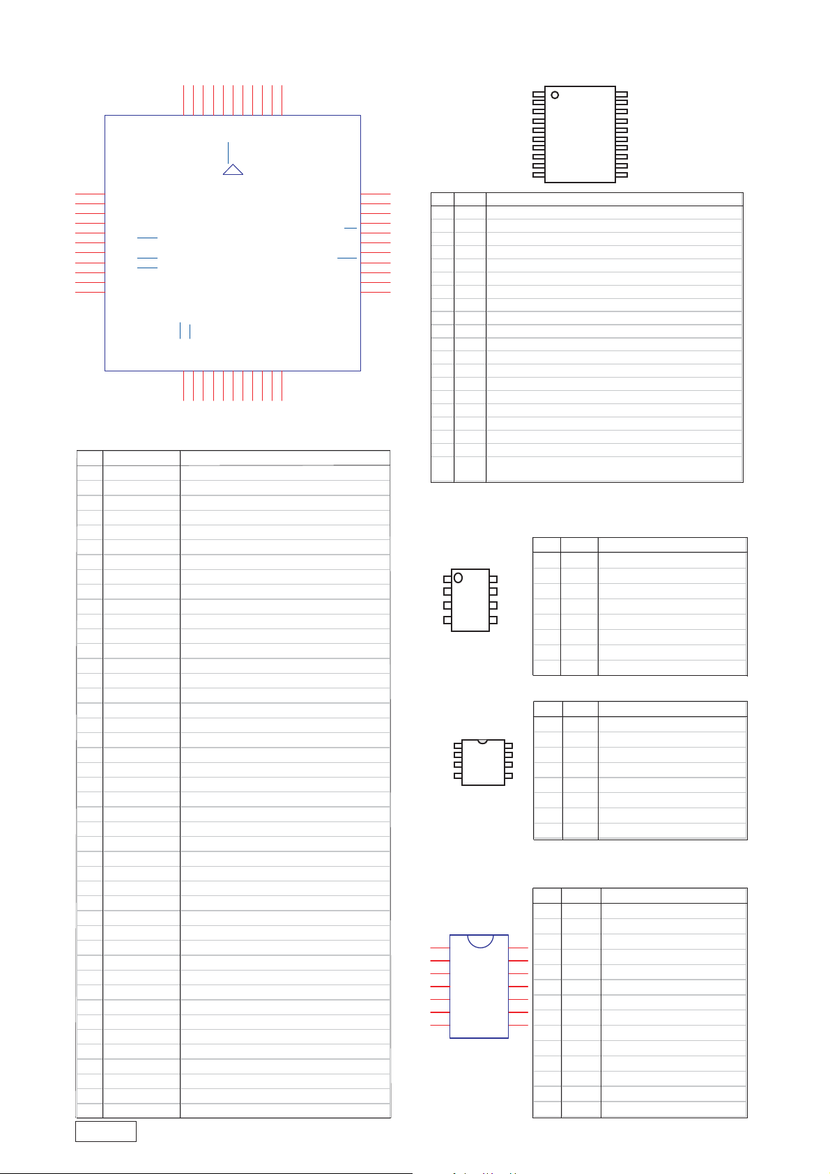
■ELECTRICAL PART LIST
MAIN BOARDASS'YSection
VMA770
VMA773
- 6-
Page 7

- 7-
VMA770
VMA773
Page 8

VMA770
VMA773
- 8-
Page 9

PHONE BOARDASS'Y Section(PC06119-32A-1R)
- 9-
VMA770
VMA773
Page 10

EXPLODED VIEW / PARTSLIST
REF PART No DESCRIPTION Q'TY
1 PL-1005-0102A-1R IR Cover HLM-0561/0706 1
2 PL-1001-0047-1R Front cover HLM-0706(VMA770) 1
2 PL-1001-0041-1R Front cover HLM-0706(VMA773) 1
3 PL-1001-0075A-1R IR Lens HLM-0561/0706 1
4 QM-01-2002 Screw M2.0*2.0 1
5 PL-1007-0076-1R Power Li ghtHLM-0561/0706 1
6 PL-1006-0092-1R Control key 1part HLM-0706 1
7 PL-1006-0093-1R Control key 2part HLM-0706 2
8 QM-01-2504 Screw M2.5x4 2
9 LD-0701-03A-1R LCD PanelA070FW03 1
10 MZ-0003-06-1R Insulator 20x20x0.5 HLM-0706 1
11 PA2B612003-1R Cushion 14x8x2.5 2
12 HD-0500-08-1R Insulator HLM-0706 1
13 MS-0706-04-1R Left-BKT HLM-0706 1
14 QM2A603-82-1R Screw M2.6x3 2
15 Main / Phone Bord Ass'y 1
16 QT-21-2606A Screw TP2.6x6 6
17 MS-0561-04-1R Cabele BKT HLM-0561/0706 1
18 PL-1002-0028-1R Rear Cover HLM-0706 1
19 QM2A605-86-1R Screw M2.6*5 black 1
20 QT2A606-16 Screw M2.6*L6 black 1
21 MS-0706-05-1R Stand BKT HLM-0706 3
22 PA2B617005-1R Insert Card HLM-0706(VMA770) 1
22 PA2B612005-1R Insert Card HLM-0706(VMA773) 1
23 QT-0206-26-1R Screw TP2.0x6 black 6
24 PL-1007-0074-1R Bucket Monitor HLM-0706 1
BLOCK DIAGRAM
I/O
AUX CVBS
AUX IN
AUX CVBS
AUXAUDIO
AV IN
AV CVBS
AV AUDIO
HEADPHONE
EARAUDIO OUT
IR LED
IRAUDIO OUT
DC JACK
DC12V
VMA770
VMA773
AV CVBS
IR
KEY
AUXAUDIO
AV AUDIO
MCU
EEPROM
24C16
VIDEO
SCALER
TW8806
MCU
IC5964
AUDIO
AUDIO
SWITCH
PI5C3309
VCOM
VGH
VGL
AUDIO
VOLUME
CONTROL
PT2259
AUDIO
OPAMP
BA4558
- 10 -
BA4558
74HC14
74HC14
AUDIO
OPAMP
TS488
IR TRANS
HS2K219
LCD Panel
7" AU A070FW03
EARAUDIO OUT
IRAUDIO OUT
DC12V
5V STB
INVERTER
INVERTER
MP1010B
SWITCHING
REGULATOR
FP5001
XN4601
ST4435
LINEAR
REGULATOR
LD117A
LINEAR
REGULATOR
LD117A
POWER
LCD Panel
7" AU A070FW03
5V STB
3.3V
1.8V
Page 11

J
I
H
G
F
E
D
BC
A
CIRCUIT DIAGRAM
7
MAIN VIDEO section
to P.1 4
to P.1 4
VSS
FILT
PGND
HSYNC
AVSS
PVDD
AGND2
AVDD
DVDD
AVDD2
AVDD3
AGND3
DTV23
DTV22
DTV21
DTV20
DTV19
VSS33
VSS18
DTVVS
DTVHS
DTVDE
DTVC
EXT_CK/VSYNC
V
V
6
to LCD
to P.1 2P.14
SDAT
to P.1 2P.14
to P.1 3P.14
TW_R EST
to P14
5
8
3
G2
G3
G4G5G6
R2
R3
R4R5R6
R7
DD18
G0/CP1+
R0/CP0+
R1/CP0-
VSS3
DD33
PVS/TRSPT
PDE/TROE
PHS/TCSPL
G7
G1/CP1-
DD33
7
6
5
4
3
to P.1 4
2
4
3
2
1
J
I
H
- 11 -
VMA770
VMA773
E
DG
BC
A
1
Page 12

A
MAIN AUDIO section
7
6
to P. 14
to P. 14
B C
AUDI O_SET
to P. 14
D
E
F
G
H
I
J
7
to P. 11P.1 4
EO_L
to P. 14
6
AUDIO _SET
to P. 14
to P. 14
to P. 14
AUDI O_SET
to P. 14
5
to P. 11P.1 4
4
IR_S EL1
IR_S EL2
3
to P. 14
to P. 14
to P. 14
AUDIO _SET
to P. 14
EO_R
5
to P. 14
4
3
2
1
A
B C
- 12 -
VMA770
VMA773
E
F
G
H
I
2
1
J
Page 13

J
MAIN POWER section
7
to P. 14
to P. 14
6
I
H
G
F
E
D
BC
A
7
EO_L
to P. 14
AUD IO_SEL
to P. 14
AUDI O_SCL
to P. 14
6
to P. 14
to P. 14
AUD IO_SEL
to P. 14
to P. 11P.1 4
5
4
IR_S EL1
IR_S EL2
to P. 14
3
to P. 14
to P. 14
AUDI O_SDA
to P. 14
EO_R
to P. 14
5
4
3
2
1
J
I
H
- 13 -
VMA770
VMA773
E
DG
BC
A
2
1
Page 14

A
MAIN MCU & IO section
7
Pigtail Cable
P2
6
5
2
5
8
7
P2
No
Description Function
1
AUDIO L Audio left channel Input
2
AUDIO GND Audio Ground
AUDIO R Audio right channel Input
3
AUDIO GND Video input port Ground
4
5
VIDEO Video input port
GND Power Ground
6
IR IR data output
7
8
ACC +12V ACC + 12V Power Input
GND Power Ground
9
ZD7
NC
5VSTB
to P14
to P14
IR_IN
IR
SCL
SDA
F
U1
AP1702
1
5VSTB
G
H
I
J
7
SCL
to P14
SDA
TW_RESET
PDN_XTAL
to P12
to P12
to P12
to P12
10
11
12
13
14
15
16
17
7
8
9
U2
P1.5
P1.6
P1.7
RST
P3.0 / RXD
P4.3 / INT2
P3.1 / TXD
P3.2 / INT0
P3.3 / INT1
P3.4 / T0
P3.5 / T1
to P12
to P12
C8
22pF
Y1
27MHz
5VSTB
12345
6
P1.2
P1.3
P1.4
VCC
T2/P1.0
AD1/P0.1
AD0/P0.0
INT3/P4.2
T2EX/P1.1
SM5964
P3.6 / WR
P3.7 / RD
XTAL2
XTAL1
GND
P4.0
P2.0 / A8
P2.1 / A9
C9
22pF
P2.2 / A10
1819202122232425262728
PWR
to P13
INV_EN
to P13
PANEL_EN
to P11
4041424344
AD3/P0.3
AD2/P0.2
39
AD4 / P0.4
38
AD5 / P0.5
37
AD6 / P0.6
36
AD7 / P0.7
35
EA
34
P4.1
33
ALE
32
PSEN
31
A15 / P2.7
30
A14 / P2.6
29
A13 / P2.5
P2.3 / A11
P2.4 / A12
SW1 TACT_SW
SOURCE
SW2 TACT_SW
DOWN
SW3 TACT_SW
UP
SW4 TACT_SW
MENU
SW5 TACT_SW
POWER
SCLK
SDAT
AUDIO_SCL
AUDIO_SDA
23
OUTVCC
GND
TC1
NC
R7
NC
to P14
MUTE
AUDIO_SEL
RST
RX
TX
IR_IN
to P14
INV_RESET
to P11
to P11
R211 NC
R6 4K7
INV_SW
IR_SEL1
IR_SEL2
IR_EN
5VSTB
5VSTB
to P13
to P12
to P12
to P12
SOURCE
DOWN
UP
MENU
POWER
PDN_XTAL
TW_RESET
TX
RX
SDA
MUTE
AUDIO_SEL
SCL
AUDIO_SDA
AUDIO_SCL
SDAT
SCLK
PWR
INV_EN
PANEL_EN
INV_SW
IR_SEL1
IR_SEL2
IR_EN
6
7
8
6
7
8
8
7
6
8
7
6
8
7
6
8
7
6
RN1
4K7 X 4
RN2
4K7 X 4
RN3
4K7 X 4
RN4
4K7 X 4
RN5
4K7 X 4
RN6
4K7 X 4
5VSTB
PWR
45
3
2
1
45
3
2
1
1
2
3
45
1
2
3
45
1
2
3
45
6
5
1
2
3
45
DC12V
A K
to P14
INV_RESET
D2
SK34
D
IR
R1
4K7
ZD1
5V1_ZENER
R5
10K
B
R8
3K3
AUX_V
to P11
CE
C4
0.1uF
Q2
2N3904
R2
22K
C3 0.1uF
U3
1
S0
2
S1
3
S2
4 5
GND SDA
24C16
B C
P1
1
J1
+12V
GND
GND
IR
AUX_V
AUX_L
AUX_R
GND
JST-8PIN-2.0P
1
2
3
4
5
6
7
8
3AF1
A
L33
FB601_3A
D12
D11
NC/LDP24A
NC/LDP24A
VCC12 5VSTB
4
3
+
EC12
NC
L1
FB601_3A
C1
0.1uF
R104
4K7
ZD2
6V8_ZENER
R198
4K7
6
R199
9
5K6
L2 FB080
C5
100pF
D1
SK34
A K
C2
0.1uF
R105
4K7
CE
B
Q21
2N3904
D3 SK34
A K
C6
100pF
Q1
1
S
2
S
3
SGD
4
SI4435DY
VCC
WC
SCL
D
D
D
8
7
6
E
VCC12
8
7
6
5
2.0mm_4PIN
5VSTB
R3 33
R4 33
IR1
IRM-4838F4
VCC
GND
OUT
5VSTB
J2
1
TX
2
RX
3
4
to P12
SCLK
R204
0
R201 NC
R202 NC
R203
0
SDAT
to P12
5VSTB
R10
R9
4K7
100
3
2
1
C7
0.1uF
R11 33
R12 33
L3 FB601
4
J3
1
R1_OUT
2
L1_OUT
3
3
Headphone Jack
AV IN Jack
GND1
GND1
AUX_L
AUX_V
GND2
GND3
AUX_R
9PIN_2.0p_DIP
4
5
6
7
8
9
ZD8
NC
ZD9
NC
A
R13
4K7
A
R15
4K7
A
R17
NC
C10
100pF
L4 FB601
C12
100pF
L5 FB601
C14
2200pF
L6 FB601
Headphone Jack
C16
R21
4K7
A
R19
NC
R23
4K7
2200pF
L7 FB601
C18
100pF
L8 FB601
C20
100pF
Symbol Function
L1_OU T Au di o left ch an ne l input
R1_OU T Au di o right c ha nn el i npu t
GND GRO UN D
2
1
AV IN Jack
Symbol Function
AUX_L A ud io l eft cha nn el i np ut
AUX_R A ud io r ight ch an ne l in put
GND GRO UN D
AUX_V V id eo c hanne l In pu t
ZD6
ESD
ZD3
ESD
ZD4
NC
ZD5
NC
R235 0
R236 0
C15
100pF
C17
100pF
R233 1K
R234 1K
R18
NC
R20
NC
C11
100pF
C13
100pF
C19
100pF
C21
100pF
AV_V
EO_R
EO_L
R22
NC
R24
NC
R14
NC
R16
NC
to P11
to P12
to P12
AV_R
AV_L
AUX_L
AUX_R
to P12
to P12
to P12
R223 0
R224 0
to P12
R225 0
R226 0
R227 0
Bottom Link
STEP 1
a. Set DC Vo lt ag e as 1 3. 2V a nd turn on th e po we r sw it ch o f the power s up pl ie r.
b. HLM-05 61 w il l po we r on a utomati ca ll y an d in O SD m ode, disp la y wh it e “AV1”w or d
and blue ba ck gr ou nd .
STEP 2.
Adjustm en t th e Vp -p v ol tage of Vco m as 5 .0 V.
STEP 3.
Adjustm en t th e VD C vo lt age of Vc om a s 1. 8V:
STEP 4.
Continu al ly p re ss “ SW 4” butt on t o di sp la y IR O FF mode, an d pr es s “S W2 ” or “ SW3”t o
display :
IR A:
L: the fr eq ue nc y of c ha nn el is 2.3 ±0 .0 08 MH z.
R: the fr eq ue nc y of c ha nn el is 2.8 ±0 .0 08 MH z.
IR B:
L: the fr eq ue nc y of c ha nn el 3.2± 0. 00 8M Hz .
R: the fr eq ue nc y of c ha nn el 3.8± 0. 00 8M Hz .
STEP 5.
a. Press “S W1 (S OU RC E)” butto n to c ha ng e to AV1 mode :
b. AV sel ec to r bo x wa s switche d to AV1 c ol or bar to ins pe ct i f th e ou tp ut screen i s
A A
GND
R228 0
R229 0
R230 0
normal. c . Pr es s “S W3 ”and adju st t he (▲) v ol um e to 3 0 to inspec t th at t he w av e
patte rn o f CH 1 an d CH 2 on t he oscill os co pe o f th e ou tput soun d ar en ’t d is to rted.
d. Press “S W1 (S OU RC E)” butto n to s wi tc h to A V1 2mode:
e. AV sel ec to r bo x wa s sw itched to A V2 c ol or b ar t o in spect if th e ou tp ut s cr ee n is
normal.
f. Insp ec t th at t he w av e pattern o f CH 1 an d CH 2 on t he o scillos co pe o f th e ou tp ut
R231 0
R232 0
PWB adjustment working steps
STEP 6.
Wireles s ea rp ho ne s te st:
a. Press “S W1 ( SO UR CE )” button t o ch an ge t o AV 1 mo de and the AV s el ec to r bo x wa s
switche d to A V1 D VD m od e.
b. Contin ua ll y pr es s “S W3” til l IR m od e di sp la yed on OSD an d pr es s “S W2 ” or “ SW1” to
select IR A , IR B o r IR o ff m od e.
c. If sel ec t IR A m od e an d th en the sele ct ed c ha nn el o f wireles s ea rp ho ne s mu st be A
to make sur e if t he o ut pu t sound is no rm al .
d. If sel ec t IR B m od e an d th en the sele ct ed c ha nn el o f wireles s ea rp ho ne s mu st be B
to make sur e if t he o ut pu t sound is no rm al .
e. If sel ec t IR O FF m od e; i nfrared r ay s wi ll b e of f. T here is no so un d ou pu t.
STEP 7.
Remote co nt ro ll er t es t:
a. Press“ SW 2 (S OU RC E) ” butto n to c ha ng e to A V1 m ode and the A V se le ct or b ox w as
switche d to A V1 m od e.
b. Use th e cl ar io n’ s re mo te cont ro ll er a nd c he ck i f the fun ct io ns a re n or mal.
STEP 8.
Press“S W5 ( PO WE R) ” an d HLM-056 1 wi ll p ow er o ff a nd then L ED 1 li gh t of f.
Notic e:
1.Out pu t ea rp ho ne s: use 33 Ω loa di ng .
2.TV ty pe ( Eu ro pe ): s et video pa tt er n as PAL and D VD p layer as NT SC .
TV type ( US A) : se t vi de o pattern a s NT SC a nd D VD p la yer as PAL .
3. Th e in sp ec to rs must wea r ES D ri ng .
4
3
2
1
sound are n’ t di st or te d.
A
A
B C
- 14 -
VMA770 VMA770
VMA773 VMA773
E
F
G
H
I
J
Page 15

J
I
H
G
F
E
D
BC
A
PRINTED WIRING BOARD 1 of 2
7
Q19
Q
U U7
Q18
U17
Q20
Q2
Q22Q17
Q1
Q12
Q11
U8
Q23
U15
U11
Q10 Q1 6
Q15
Q13
U2
Q21
U13
U12
U3
U14
Q13
Q8
Q7
U10
Q6
Q14
U16
U19
Q9
U9
U6
U4
Q5
U18
TOP VIEW (REAR COVER SIDE)
6
5
7
6
5
4
3
Pigtail Cable
4
3
1
2
5
8
2
1
P2
No
7
1
2
3
4
5
6
7
8
9
4
3
6
9
Description
AUDIO L
AUDIO GND
AUDIO R
AUDIO GND
VIDEO
GND
IR
ACC +12V
GND
2
1
AV IN Jack
J
I
H
F
E
DG
BC
Headphone Jack
A
- 15 -
Page 16

A
PRINTED WIRING BOARD 2 of 2
7
B C
D
E
F
G
H
I
J
7
6
5
4
6
5
4
3
2
MENU
1
Headphone Jack
A
AV IN Jack
B C
D
E
SOURCE
F
POWER
G
IR
H
I
3
2
1
J
- 16 -
VMA770
VMA773
 Loading...