

Page 1

WK-1800
INDEX
MAY.2000
FULL RANGE
CHORD
MAX
FINGERED
CASIO CHORD
MIN
SONG
PATTERN
EXTERNAL
CH 4
CH 5
CH 6
CH 7
CH 8
CH 9
CH 10
CH 11
CH 12
CH 13
CH 14
CH 15
CH 1
CH 2
CH 3
INTERNAL
ACC VOL.
CHORD1
CHORD2
CHORD3
BASS
UPPER1
UPPER2
LOWER1
RHYTHM
LOWER2
CH 16
PARAMETER RESET:
MAIN MANU/
TR1
CHANNEL VOLUME:
TR2
TR3
TR4
TR5
TR6
SUB MANU/
CHANNEL SELECT:
STOREBANK
789
456
1023
DELETE
AMP ENVELOPE
DECAY
SUSTAIN
PITCH ENVELOPE
00 FLAT
01-17 VIBRATO
/YESS/NO
18-45 OTHERS
WK-1800
HIGH-GRADE KEYBOARD
Ver.1 : Apr. 2007
Page 2

CONTENTS
Specifications ---------------------------------------------------------------------------------------------- 2
Important Operation ------------------------------------------------------------------------------------- 4
Block Diagram --------------------------------------------------------------------------------------------- 5
Circuit Description --------------------------------------------------------------------------------------- 6
Diagnostic Program------------------------------------------------------------------------------------ 22
Major Wa veformes -------------------------------------------------------------------------------------- 28
Printed Circuit Board ---------------------------------------------------------------------------------- 29
Exploded View ------------------------------------------------------------------------------------------- 34
Parts List--------------------------------------------------------------------------------------------------- 35
Schematic Diagrams----------------------------------------------------------------------------------- 38
— 1 —
Page 3

SPECIFICATIONS
GENERAL
Keyboard: 76 standard-size keys , 6 octav es (with touch response on/off; ExLight/
Light/Normal/Heavy touch)
Tones: 232 (128 General MIDI, 64 variation, 8 drum, 32 user); with layer and
split
Rhythm instrument tones: 53
Polyphony: 32 notes maximum (16 for certain tones)
Digital effects: 10 (REVERB 1, 2, 3; CHORUS; TREMOLO; PHASE SHIFTER; OR-
GAN SPEAKER; ENHANCER; FLANGER; EQ LOUDNESS)
Auto accompaniment
Rhythm patterns: 130 (120 + 10 user rhythms)
Tempo: Variable (226 steps, = 30 to 255)
Chords: 3 fingering methods (CASIO CHORD, FINGERED, FULL RANGE
CHORD)
Rhythm controller: Start/Stop, Intro, Normal/Normal Fill-In, Variation/Variation Fill-In,
Synchro/Ending
Accomp volume: 0 to 127 (128 steps)
One touch presets: Recalls settings for tone, tempo, layer , and Auto Harmonize in accor-
dance with rhythm.
Auto harmonize: Automatic addition of notes that harmonize with melody note in ac-
cordance with specified Auto Accompaniment chords.
Free session
Number of patterns: 120 (Auto Accompaniment function based on preset chord progres-
sions.)
Song sequencer
Songs: 2
Recording tracks: 6 (2 through 6 are melody tracks)
Recording method: Real-time
Memory capacity
(total for two songs): Approximately 8,000 notes
Punch in: Supported
Pattern sequencer
Number of patterns: 10 (Rhythm numbers 120 to 129)
Memory capacity: Approximately 6,800 notes
Elements: Intro, Normal, Variation, Normal Fill-In, Variation Fill-In, Ending
Parts: Chord 1, 2, 3; Bass; Rhythm
Recording method: Real-time
Registration memory
Number of setups: 20 (5 setups × 4 banks)
Memory contents: Tone, Rhythm, Tempo, Split on/off, Split point, Layer on/off, Auto Har-
monize on/off, Mixer settings, Keyboard channel on/off, DSP (digital
effect) on/off, DSP (digital effect) settings, Accompaniment mode,
Touch Response settings, Assignable jack setting, Transpose, Tun-
ing, Pitch Bend range, Sound range shift on/off
Demo tunes: 2
Synthesizer
Parameters: PCM set, amp envelope set, attack rate, release rate, pitch envelope
set, pitch, level, touch sensitivity, pan, filter sensitivity, filter le v el, trans-
pose
Mixer
Channels: 32(Internal 16, External 16)
Modes: Internal, External, External/Solo, External/Play
Parameters: Program change number, volume, expression, pan, coarse tuning,
fine tuning, Effect Send
MIDI: 16-channel multi-timbre receive, General MIDI Level 1
— 2 —
Page 4

Other functions
Pitch bend range: Adjustable (12 semitones upwards and downwards)
Modulation: Equipped
Transpose: 25 steps (–12 semitones to +12 semitones)
Tuning: Adjustable (A4 = approximately 440Hz ± 50 cents)
Terminals
MIDI terminal: IN, OUT
Sustain/Assignable jack: Standard jack (sustain, sostenuto, soft, rhythm start/stop)
Line out L(MONO)/R
Output Impedance: 3 kΩ
Output Voltage: 1.5 V (RMS) MAX
Headphones Stereo standard jack
Output Impedance: 200 Ω
Output Voltage: 220 mV (RMS) MAX
12 V DC
Floppy disk drive
Type: 3.5" FDD
Formats: 2DD (720KB MS-DOS format)
2HD (1.44MB MS-DOS format)
Functions: Save and load of user tones, user rhythms, sequencer, and registration
data; playback of SMF; disk formatting; file delete; accompaniment pat-
tern style conversion
Power supply: Dual power supply system
Batteries Six D-size batteries
Battery life Approximately 2 hours continuous operation on alkaline batteries
AC adapter: AD-12
Auto power off: Turns power off approximately six minutes after last key operation. En-
abled under battery power only, can be disabled manually.
Speaker output: 5 W + 5 W
Power consumption: 12 V 18 W
Dimensions: 122.5 × 42.3 × 16.7 cm (48 1/4 × 16 11/16 × 6 9/16 inch)
Weight (without batteries): Approximately 9.8 kg (21.6 lbs)
Standard accessories: Music Stand; Pattern Conversion Disk
ELECTRICAL
Current drain with 12 V DC:
No sound output 480 mA ± 20 %
Maximum volume 1765 mA ± 20 %
with 24 keys from C3 to B4 pressed in Synth-Bass 4 tone
Volume: MAX., Velocity: MAX.
DSP0: Reverb1
Phone output level (Vrms with 32 Ω load each channel):
with tone Synth-Bass 4 tone L-ch (Key C3) 590 mV ± 20 %
Volume: MAX., Velocity: MAX. R-ch (Key F3) 590 mV ± 20 %
DSP0: Reverb1
Speaker output level (Vrms with 8 Ω load each channel):
with tone Synth-Bass 4 tone L-ch (Key C3) 7900 mV ± 20 %
Volume: MAX., Velocity: MAX. R-ch (Key F3) 7350 mV ± 20 %
DSP0: Reverb1
Output level (Vrms with 47 kΩ load each channel):
with tone Synth-Bass 4 tone L-ch (Key C3) 605 mV ± 20 %
Volume: MAX., Velocity: MAX. R-ch (Key F3) 510 mV ± 20 %
DSP0: Reverb1
Minimum operating voltage: 6.1 V
— 3 —
Page 5

IMPORTANT OPERATION
Full Initialization
Use this procedure to return all keyboard settings to what they were when you purchased it. Note that this
procedure clears all data from memory.
• While holding down the ENTER button, turn on keyboard power.
Res
• Press YES to initialize the keyboard or NO to turn on power without changing any settings.
Parameter Initialization
Use this procedure to return all keyboard settings to what they were when you purchased it. Note that this
procedure does not affect user tones, user rhythms, registration memory contents, and display contrast
settings.
• While keyboard power is on, press the [+], [–], and ENTER buttons at the same time.
Adjusting Display Contrast
• Display contrast can be adjust to one of 100 levels for easy viewing.
• Adjusting display contrast helps to make figures easier to read from any viewing angle.
• Within five seconds after pressing the CONTRAST button, press [+] to increase the contrast value (making the display darker) or [–] to decrease it (making the display lighter).
• After you release CONTRAST, the message “Contrast” remains on the display for a few moments, during
which you can change the contrast setting further using [+] and [–] or by inputting a contrast value with the
number keys.
The contrast can be set to a value from 0 to 99. The initial default setting is 50.
et?
GM (General MIDI):
General MIDI standardizes MIDI data to play music with same nuance between different MIDI instruments.
Among GM conformed MIDI instruments, or commercially available musical data, music can be played with
similar tones.
SMF (Standard MIDI File):
SMF is a standard file format for MIDI instruments and computer music software. SMF formatted data can
be played and transported easily among SMF complied instruments or musical data of different manufacturers.
— 4 —
Page 6

BLOCK DIAGRAM
ROM1
LHMN5KPP
LSI1 (32Mbit)
LHMN5KPN
LSI2 (32Mbit)
RA0 ~ RA21
RD0 ~ RD15
Working
RAM
TC55257
GFL-70L
LSI4
(256Kbit)
ROM2
EA0 ~ EA14
ED0 ~ ED8
ECEB, EOEB
EWEB
Keyboard
SI0 ~
SI9
FI0 ~
FI9
KC0
~
KC7
Key Controller
TC190C020AF-001
LSI6
RD, HWR,
LWR
D0 ~ D15
SORP, SYOB, WOK1, BOK
RESB
A0 ~ A3
DSP
D8 ~ D15 RESET
HG51B155FD
RD,
LSI3
HWR
BOK
D/A Converter
µPD63200GS
LSI5
RESB
A1 ~ A4
IN
MIDI
OUT
SED1278F2A
PBO
HD6433048SA89F
D0
~
D7
TC551001CF-70L
LSI7 (1Mbit)
CE1
LCD Driver
LSI601
LDB4
~LDB7
CONT,
LRS,
LR/L
LE
CPU
LSI9
RAM1
LWR, RD CE1 HWR, RD
SEG1 ~ SEG40
LCD
COM1 ~ COM16
LEDCK, LEDCL
S-Register
TC74HC164
IC401
LSDT
SWCK
S-Register
TC74HC164
IC402
KI0 ~ KI7
NMI
TEND, DREQ, CS2, CS3, 8/5
RD, HWR, LWR
A0 ~ A15
D0 ~ D15
D8
VBR VBR
~
D15
RAM2
TC551001CFL-70L
LSI8 (1Mbit)
Back Light
LEDA ~ LEDH
KC0 ~ KC7
Chip Selector
TC74HC08
RD, HWR,
IC4
LWR
Back Light Driver
TE-CFL733-IMI
Q601, Q602
LEDs
D8
~
D15
FDD Controller
HWR
RD
HD63266F
Buttons
VDD
Out put
LPF
(L)
LPF
(R)
Main
Volume
Power Amp.
LA4663
IC201
(L) (R)
Speakers
Reset IC
RN5VD40A
IC5
VDDVC
— 5 —
IC6
Power Supply Circuit
Q209,
Q213
IC202, Q207
Q208, Q211, Q214,
Q215
LSI10
RESET
AVDDAVCCDVDDFVDDCVDDVCC
VDD
VBR
Back up
Power
3.5" FDD Unit
DF354H064C
CR2032
APO
Page 7

CIRCUIT DESCRIPTION
KEY MATRIX
KC0 KC1 KC2 KC3 KC4 KC5 KC6 KC7
FI0 E11 F11 F#11 G11 G#11 A11 A#11
SI0 E12 F12 F#12 G12 G#12 A12 A#12
FI1 B11 C21 C#21 D21 D#21 E21 F21 F#21
SI1 B12 C22 C#22 D22 D#22 E22 F22 F#22
FI2 G21 G#21 A21 A#21 B21 C31 C#31 D31
SI2 G22 G#22 A22 A#22 B22 C32 C#32 D32
FI3 D#31 E31 F31 F#31 G31 G#31 A31 A#31
SI3 D#32 E32 F32 F#32 G32 G#32 A32 A#32
FI4 B31 C41 C#41 D41 D#41 E41 F41 F#41
SI4 B32 C42 C#42 D42 D#42 E42 F42 F#42
FI5 G41 G#41 A41 A#41 B41 C51 C#51 D51
SI5 G42 G#42 A42 A#42 B42 C52 C#52 D52
FI6 D#51 E51 F51 F#51 G51 G#51 A51 A#51
SI6 D#52 E52 F52 F#52 G52 G#52 A52 A#52
FI7 B51 C61 C#61 D61 D#61 E61 F61 F#61
SI7 B52 C62 C#62 D62 D#62 E62 F62 F#62
FI8 G61 G#61 A61 A#61 B61 C71 C#71 D71
SI8 G62 G#62 A62 A#62 B62 C72 C#72 D72
FI9 D#71 E71 F71 F#71 G71
SI9 D#72 E72 F72 F#72 G72
Note: Each key has two contacts, the first conatct 1 and second contact 2.
Key
Second contact 2
First contact 1
NOMENCLATURE OF KEYS
C2 C3 C4 C5 C6 C7 G7E1
— 6 —
FI
KC
SI
Page 8
BUTTON MATRIX
KI0
KC0
KC1
KC2
KC3
KC4
KC5
KC6
KC7
PWSW POWER
MODE
RECORD
SONG
PATTERN
DSP
CON-
TRAST
FREE
SESSION
ONE TOUCH
PRESET
V ARIATION/
KI1
INTRO
NORMAL/
FILL-IN
FILL-IN
SYNCHRO/
ENDING
START/
STOP
TEMPO
▼
TEMPO
▲
BANK
KI2
MIXER
SELECT
UPPER1
CH1
UPPER2
CH2
LOWER1
CH3
LOWER2
CH4
ACC V OL
CH5
CHORD1
CH6
CHORD2
CH7
KI3
CHORD3
CH8
BASS
CH9
RHYTHM
CH10
TR1
CH11
TR2
CH12
TR3
CH13
TR4
CH14
TR5
CH15
KI4
A
B
C
D
E
STORE
TRANSPOSE
▼
TRANSPOSE
▲
HARMONIZE
KI5
TR6
CH16
AUTO
ENTER
▲
▼
DISK
KI6
SPLIT
LAYER
RHYTHM
TONE
0
1
4
7
KI7
▼/NO
—
2
5
8
▲/YES
+
3
6
9
KI8
DEMO
SYNTH
TUNE/
MIDI
TOUCH
RESPONSE
LED MATRIX
LED-A
FULL RANGE
CHORD
LED-B
FINGERD
LED-C
CASIO CHORD
— 7 —
Page 9
MEMORY DEVICES
Each memory device has the following data.
CPU
Internal Memory
3
ROM
512 kbit
4
RAM
16 kbit
LSI9
DSP
LSI3
Working RAM
7
256 kbit
LSI4
RAM1
1
1 Mbit
LSI7
RAM2
2
1 Mbit
LSI8
ROM1
5
32 Mbit
LSI1
ROM2
6
32 Mbit
LSI2
1 RAM1 :
S-RAM for operation program, Register, Pattern, Song
and SMF data from FDD. (Lower part of data bus)
2 RAM2 :
S-RAM for operation program, Register, Pattern, Song
and SMF data from FDD. (Upper part of data bus)
3 Internal ROM of CPU :
Main program data for system operation
4 Internal RAM of CPU :
Work area for system operation
5 ROM1 :
Demo, Accompaniment data, Song, P attern, Synth, Disk
mode
6 ROM2 :
Sound Waveforms/Tone data Digital sound effect
7 Working RAM :
Work area for DSP
RESET CIRCUIT
VDD
From power switch
Battery set
RESET
PWSW
VDD
RES
CPU
HD6433048SA89F
LSI9
NMI
PB0
PA7
RESET
APO
FDD Controller
HD63266F
LSI10
RESET
PW/SW ON
RESET
APO
DVDD
(5V)
Power Supply
Circuit
DVDD
HG51B155FD
Key Controller
TC190C020AF-001
DVDD
DVDD
DSP
LSI3
RESB
DVDD
RESB
LSI6
Initial reset
When batteries are set or an AC adapter is connected, the reset IC provides a low pulse to the CPU.
When the power switch is pressed, the CPU receives a low pulse of POWER signal. The CPU first raises
APO signal to +5 V to generate DVDD voltage, then raises RESET signal to +5 V. During this period the
DSP, the key controller and FDD controller LSIs initialize their internal circuits.
— 8 —
Page 10
POWER SUPPLY CIRCUIT
The power supply circuit provides various voltages as shown below.
The voltage VDD (+5 V) is provided as long as batteries or AC adaptor is set.
Other voltages are controlled by APO (Auto Power Off) signal from CPU.
LC Filter
(To digital)
(To FDD)
(To LCD)
NMI
APO
PW/ON
APO
(To analog)
CPU
HD6433048SA89F
PA7
LSI9
NMI
PW/SW
The regulator IC BA9700A generates square waveform from pin 5 as PWM (Pulse Wide Modulation).
The LC filter makes stable output voltage (+5 V) for each circuit as shown above.
— 9 —
Page 11

DSP and DAC CIRCUIT
RA22
Working RAM (256K-bit)
TC55257DFL-70L
LSI4
ROM2
LHMN5KPN
LSI2 (32Mbit)
ROM1
LHMN5KPP
LSI1 (32Mbit)
BOK
EA0 ~
EA14
D0 ~
D15
ED0 ~
ED15
KC0 ~
KC7
SI0 ~ SI9
FI0 ~ FI9
RA0 ~
RA21
RA0 ~ RA21
CS
RA23
CE,OE
A0 ~ A20,NC
Q0 ~ Q15
CE,OE
A0 ~ A20,NC
Q0 ~ Q15
WE
OE
D0 ~ D15
A0 ~ A14
PG
24.576 MHz
DAC
LOUT
ROUT
SORP: Sound data
BOK: Bit clock
WOK1: Word clock
CLK
SI LRCK
LRCK0
DOUT
SORP
WOK1
WOKI0 DI D0 LRCK0
DSP
HG51B155FD
LSI3
CPU
HD6433048SA89F
LSI9
Key Controller
TC190C020AF-001
LSI16
RD0 ~ RD15
RA0 ~
RA21
D8 ~
D15
Control
data
key
data
key
data
Keyboard
The DSP (Digital Signal Processor) and DAC (Digital Analog Converter) consists of the following circuits.
— 10 —
Page 12

FDD UNIT (DF354H064C)
FDD Specifications:
1 Memory Capacity (under un-format) : 1.6 MByte
2 Density of track : 5.33 track/mm (135 TPI)
3 Number of track : 77 track/side
4 Number of head : 2
5 Rate of data transfer : 500 kbps
6 Access time (between two tracks) : 3 m seconds
7 Compensation of writing data : 125 n second (all tracks)
8 Rotation speed : 360 Min-1 (rpm) ± 1.5 %
FDD Interface:
Host system Drive
CN2 connector
Drive Select 1 12
Density Select4
Index8
Motor ON 16
Direction 18
Step 20
Write Data 22
Write Gate 24
Side 1 Select 32
DC.GND
+5 V
N.C 4
System Frame GND.
Track 0026
Write Protect28
Read Data30
Disk Change34
GND Pin Numbers of CN2:
1, 5, 7, 9, 11, 13, 15, 17, 19, 21, 23, 25, 27, 29, 31, 33
Non connected Pin Numbers of CN2:
2, 6, 10, 14 (Pin #3 is removed to prevent erroneous insertion)
CN1 connector
1
+5 V Return2
+5 V Return3
0 Ω
Signal GND
— 11 —
Drive Frame GND.
Page 13
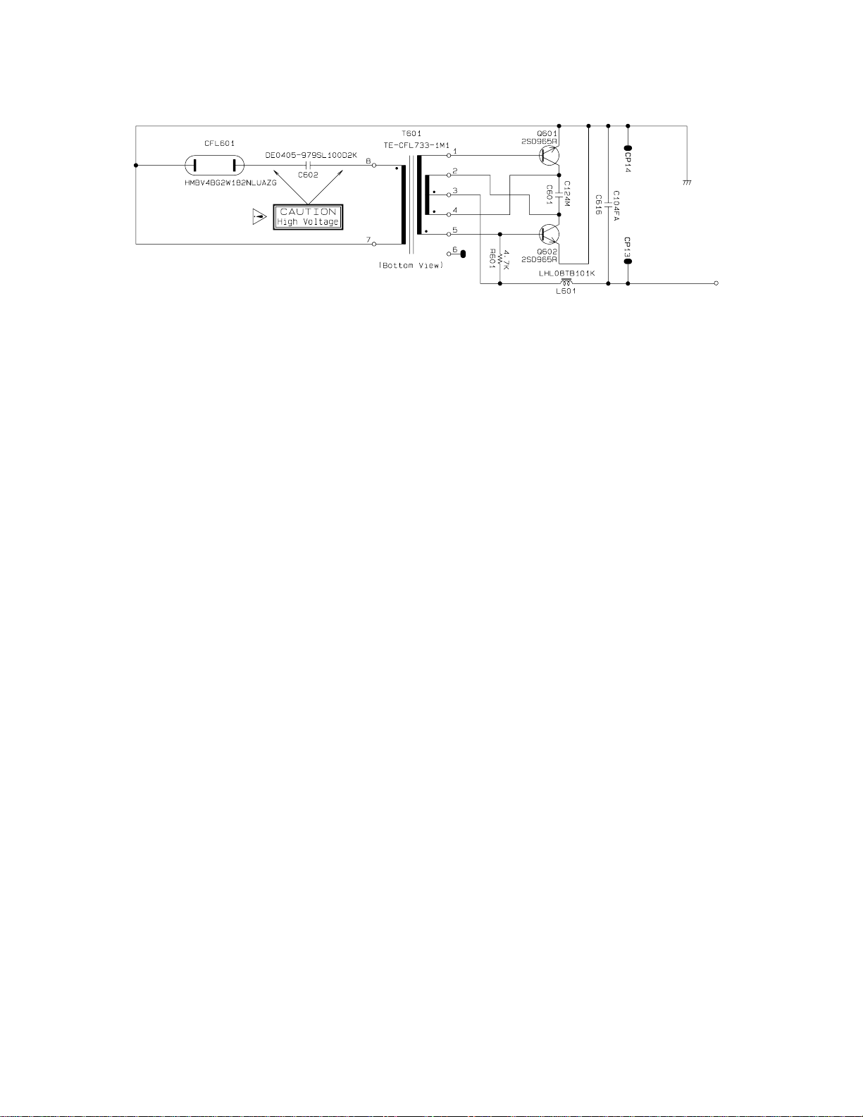
LCD BACKLIGHT
DG
CVDD
When voltage CVDD is supplied, transistors Q601 and Q602 start oscillation.
From the oscillation voltage, transformer T601 generates about 600 V which is necessary for lighting the
backlight.
— 12 —
Page 14

CPU (LSI9: HD6433048SA89F)
The 16 bit CPU contains a 1M-bit ROM, a 16K-bit RAM, eleven 8-bit I/O por ts, an A/D converter, a D/A
converter and serial interfaces. The CPU accesses to the RAM1, RAM2, DSP, Key controller, FDD controller and LCD driver LSI. The CPU also controls buttons, LEDs, bender input and MIDI input/output.
Pin No. Terminal In/Out Function
1 VCC In VCC (5 V) source.
2 ~ 5 PB0 ~ PB3 Out Data bus for LCD driver.
6 PB4 Out Chip enable signal for LCD driver.
7 PB5 Out Read/write signal for LCD driver.
8 DREQ0 — DMA (Direct Memory Access) request.
9 PB7 Out Register selection signal for LCD driver.
10 RES0 In Not used.
11 VSS In Ground terminal (0 V).
12 TXD0 Out MIDI signal output.
13, 15 ~ 17 P91, P93~P95 In Key input signal from buttons.
14 RXD0 In MIDI signal input.
18 ~ 21
23 ~ 34
D0 ~ D15 In/Out Data bus.
22 VSS In Ground terminal (0 V).
35 VCC In Vcc (5 V) source.
36 ~ 43,
45 ~ 56
A0 ~ A19 Out Address bus.
44, 57 VSS In Ground terminal (0 V).
55, 59, 60 P52, P61, P62 In Key input signal from buttons.
58 WAIT — Not used.
61 CLKOUT Out Clock signal (16 MHz).
62 STBY — Not used.
63 RES In Reset signal at VDD (5 V) supplied.
64 NMI In Power ON signal input.
65 VSS In Ground terminal (0 V).
66, 67 EXTAL, XTAL In Clock (16 MHz) input.
68 VCC In Vcc (5 V) source.
69 AS — Not used.
70 RD Out Read signal.
71 HWR Out Write signal for upper data bus.
72 LWR Out Wr ite signal for lower data bus.
73 ~ 75 MD0 ~ MD2 In Mode selection terminals.
76, 77 AVCC, VREF In Power source and reference voltage for internal A/D, D/A.
78 P70 In Key input signal from buttons.
79 AN1 In Pitch bender voltage detection.
— 13 —
Page 15

Pin No. Terminal In/Out Function
80 P72 In AC adaptor detection terminal.
81 P73 In Modulation signal input.
82 P74 In Pedal signal input.
83 P75 In FD sheet type (2HD, 2DD) signal input.
84 P76 In Key input signal from buttons.
85 DA1 Out LCD contrast control voltage output.
86 AVSS In Ground terminal (0 V).
87 PB0 Out Reset signal for DSP, Key controller, FDD controller.
88 CS3 Out Chip select signal for FDD.
89 CS2 Out Acknowledge signal FDD DMA function.
90 CS1 Out Chip select signal for Key controller.
91 CS0 Out Chip select signal for DSP.
92 VSS In Ground terminal (0 V).
93 TEND0 Out End signal for data transfer of FDD.
94 PA1 Out Change signal for data transfer speed of FDD.
95 PA2 Out Key input signal for DEMO button.
96 PA3 Out Clock signal for shift register of KC signal.
97 PA4 Out Clear signal for shift register of LED.
98 PA5 Out Control signal for KC signal and LED.
99 PA6 Out Clock signal for shift register of LED.
100 PA7 Out APO (Auto Power Off) signal.
— 14 —
Page 16

DIGITAL SIGNAL PROCESSOR (LSI3:HG51B155FD)
Upon receipt of note numbers and their velocities, the DSP (Digital Signal Processor) reads sound and
velocity data from the sound source ROM in accordance with the selected tone; the DSP can read rhythm
data simultaneously when a rythm pattern is selected. Then it pro vides 16-bit serial signals containing data
of the melody, chord, bass, and percussion to the DAC. The DSP also adds the selected effect to the sound
data using a 256k-bit RAM.
The following table shows the pin functions of the DSP.
Pin No. Terminal In/Out Function
1 ~ 8 CD0 ~ CD7 In/Out Data bus
9, 10 Not used.
11 GND7 In Ground (0 V) source
12 CK16 Out 24.576 MHz clock output
13 VCC6 In +5 V source
14 CK0 In Clock input. Connected to terminal CK16.
15 TCKB Not used.
16 VCC1 In +5 V source
17 GND1 In Ground (0 V) source
18, 19 XT0, XT1 In/Out
24.576 MHz clock input/output. Connected to a crystal oscillator.
20 SGL In System control terminal. Single chip system: Open
21 CCSB In Chip select signal input
22 ~ 25 CA0 ~ CA3 In Address bus
26 CE0 In Not used. Connected to ground.
27 CWRB In Write enable signal
28 CRDB In Read enable signal
29 ~ 32 Not used.
33 RESB In Reset signal input
34 TESB In Not used. Connected to +5 V
35 ~ 39 Not used.
40 ~ 49
52 ~ 57
RD0 ~ RD15 In Data bus for the ROM1 and ROM2
58 RA23 Out Chip select signal for the ROM1
59 RA22 Out Chip select signal for the ROM2
60 ~ 73
75 ~ 82
RA0 ~ RA21 Out Address bus for the ROM1 and ROM2
74 GND5 In Ground (0 V) source
83 WOK2 Out Word clock output. Not used.
84 VCC3 In +5 V source
85 GND3 In Ground (0 V) source
86 WOK1 Out Word clock for the DAC
87 SOLM Out Serial data output. Not used.
88 SOLP Out Serial data output for the DAC
89 BOK Out Bit clock output for the DAC
— 15 —
Page 17

Pin No. Terminal In/Out Function
90 ~ 92 Not used.
93 VCC In +5 V source
94, 95
97 ~ 105
107, 109
EA0 ~ EA14 Out Address bus for the working RAM
110, 112
96 EWEB Out Write enable signal output for the working RAM
106 EOEB Out Read enable signal output for the working RAM
108 VCC7 In +5 V source
111 ECEB Out Chip select signal output for the working RAM
113 ~ 117 Not used.
118 VCC4 In +5 V source
119 GND4 In Ground (0 V) source
120 ~ 122 Not used.
123 ~ 130 ED0 ~ ED7 In/Out Data bus for the working RAM
131 GND5 In Ground (0 V) source
132 ~ 134 Not used. Connected to ground.
135, 136 Not used.
FDD CONTROLLER (LSI10:HD63266F)
The FDD (Floppy Disk Drive) controller can control the FDD unit.
The controller contains not only analog VFO (Variable Frequency Oscillator) circuit but also driver/receiver,
input/output port and oscillation circuit internally.
Pin No. Terminal In/Out Function
1 8/ - 5 In Change of data transfer speed.
2 XTALSEL — Not used. Connected to ground (0 V).
3 RESET In Reset signal input.
4 E, -RD In Read signal.
5 R/-W, -WR In Write signal.
6 CS In Chip select signal.
7 DACK In Acknowledge signal of DMA (Direct Memory Access).
8, 9 RS0, RS1 In Register selection for read/write.
10, 11 VSS1, VSS2 In Ground terminal (0 V).
12 ~ 19 D0 ~ D7 In/Out Data bus.
20 DREQ In Request signalof DMA.
21 IRQ — Not used.
22 DEND In End signal for data transfer.
23 VSS3 In Ground terminal (0 V).
24 1/2 EX1 — Not used.
25 VCC1 In DVDD (5 V) source.
26, 27, 28
NUM1, NUM2
IFS
—
Not used. Connected to ground (0 V).
29 SFORM In Selection signal for formatting.
— 16 —
Page 18

Pin No. Terminal In/Out Function
30 INP In Disk detection signal.
31 READY In Ready signal from FDD. (Connected to ground (0V).)
32 WPRT In Write protect signal from FDD.
33 TRKO In Track0 signal from FDD.
34 INDEX In Index signal from FDD.
35 RDATA In Read data signal from FDD.
36, 37, 38
39
XTAL2, EXTAL2
NC, XTAL1
—
Not used.
40 EXTAL1 In Clock signal input from CPU (16 MHz).
41, 42 VSS4, VSS5 In Ground terminal (0 V).
43 NC — Not used.
44 ~ 46
VCC2, VCC3,
VCC4
In
DVDD (5 V) source.
47 WG ATE Out Write gate signal to FDD.
48 WDATA Out Write data signal to FDD.
49 VSS6 In Ground terminal (0 V).
50 STEP Out Step signal for FDD head.
51 HDIR Out Head direction signal for FDD.
52 HLOAD Out Not used.
53 HSEL Out Head selection signal for FDD.
54 VSS7 In Ground terminal (0 V).
55 DS0 Out Drive selection signal.
56, 57, 58
DS1, DS2, DS3
— Not used.
59 VSS8 In Ground terminal (0 V).
60 MON0 Out Motor ON signal for FDD.
61, 62, 63
MON1, MON2,
MON3
—
Not used.
64 VSS9 In Ground terminal (0 V).
— 17 —
Page 19

KEY TOUCH LSI (LSI6: TC190C020AF-001)
By counting the time between first-key input signal FI and second-key SI from the keyboard unit, the key
touch LSI detects key velocity of 256-step. Then the LSI sends the CPU the note number and its velocity
data.
Pin No. Terminal In/Out Function
1 WRB In Write signal from CPU.
2 ~ 11, 13,
14, 16 ~ 19
D0 ~ D15 In/Out Data bus.
12 VSS In Ground terminal (0 V).
15 VDD In VDD (5 V) source.
20 ~ 23 CA0 ~ CA3 In Address bus.
24 VSS In Ground terminal (0 V).
25 ~ 32, FI0 ~ FI4,
34, 35 SI0 ~ SI4
In Key input signal.
33 VDD In VDD (5 V) source.
36 ~ 38,
40 ~ 44
KC0 ~ KC7 Out Key scan signal.
39 VSS In Ground terminal (0 V).
45 VDD In VDD (5 V) source.
46 ~ 51
FI5 ~ FI7
SI5 ~ SI7
In Key input signal.
52 VSS In Ground terminal (0 V).
53 ~ 58,
60 ~ 62
FI8 ~ FI10
SI8 ~ SI10 In Key input signal (Not used).
KI0 ~ KI2
59 VDD In VDD (5 V) source.
63, 64
MODE0, MODE1
— Not used.
65 VSS In Ground terminal (0 V).
66 KCKI In Clock signal for key common/input.
67 ~ 72,
74 ~ 77
— Not used.
73 VDD In VDD (5 V) source.
78 RESB In Reset signal from CPU.
79 CSB In Chip selection signal.
80 RDB In Read signal from CPU.
— 18 —
Page 20

LCD DRIVER (LSI601: SED1278F2A)
The LCD driver can drive a dot matrix LCD having 40 segment and 16 common lines. The LSI contains 240
graphic symbols in the built-in character generator ROM, and stores 80 characters in the built-in display
data RAM. In accordance with command from the CPU, the LSI is capable of displaying up to 16 characters
simultaneously. The following table shows the pin functions of LSI 601.
Pin No. Terminal In/Out Function
1 ~ 22,
63 ~ 80
SEG1 ~ SEG40
Out Segment signal output
23 VSS — GND (0 V) source
24, 25 OSC1, OSC2 In/Out
Terminals for the built-in clock pulse generator. The external resistor connected determines the oscillation frequency.
LCD drive voltage input.
26 ~ 30 V1 ~ V5 In Those voltages are used for generating the stepped pulse of the
LCD drive signals.
31, 32 LP, XSCL — Not used
33 VDD In LVDD (+5 V) source
34, 35 FR, DO — Not used
36 RS In Data/command determination terminal.High: data, Low: command
37 R/W In Read/write terminal. High: read, Low: write
Chip enable signal.
38 E In High: enable, the writing is done at fall edge.
Low: disenable
39 ~ 42 DB0 ~ DB3 — Not used. Connected to GND (0 V)
43 ~ 46 DB4 ~ DB7 In/Out Data bus
47 ~ 62
COM1 ~ COM16
Out Common signal/output
REGULATOR IC (IC202: BA9700A)
The regulator IC controls the output voltage by PWM (Pulse Wide Modulation) with outer switching transistors and LC filters (integration circuit).
INVERT
Error
Amp
D-TIME
CONT
NON
INP
14
+–
1
1/2Vret
Triangle
Oscillator
INVERT
INP
13
2
RT CT FEED
12
30k
30k
PWM
Comparator
3
Vret
11
4
BACK
POWER
SW
10
Vret
5
OUT NC GND
NC VCC
9
Voltage
Regulator
6
8
7
— 19 —
Page 21

DAC (LSI5: UPD63200GS)
UPD63200GS is a two-channel 16-bit Digital to Analog Convertor consisting of resistor string, output
amplifier and zero offset circuit.
The DAC receives 16-bit serial data output from the DSP. The data contains digital sound data of the
melody, chord, bass, and percussion for the right and left channels. The DAC converts the data into analog
waveforms by each channel and output them separately.
Pin No. Terminal In/Out Function
1 fs SEL In Mode selection terminal. Connected to ground.
2 D.GND In Ground (0 V) source for internal digital circuit
3 Bit SEL Not used.
4 DVDD In +5 V source for internal digital circuit
5 A.GND In Ground (0 V) source for internal analog circuit
6 R.OUT Out Sound waveform output
7 A.VDD In +5 V source for internal analog circuit
8 A.VDD In +5 V source for internal analog circuit
9 R.REF In Reference voltage terminal. Connected to a capacitor.
10 L.REF In Reference voltage terminal. Connected to a capacitor.
11 L.OUT Out Left channel sound waveform output
12 A.GND In Ground (0 V) source for internal analog circuit
13 LRCK In Word clock (L/R separation signal) input.
14 LRSEL In Not used. Connected to ground.
15 SI In Sound data input
16 CLK In Bit clock input
— 20 —
Page 22

POWER AMPLIFIER (IC201: LA4663)
The power amplifier is a two-channel amplifier with standby switch.
STAND BY VCC1VCC2
875
SIGNAL
MUTE
IN1
PRE
GND
IN2
6
2
Ri=
20k Ω
3
Input amplifier
4
Input amplifier
CH 1
+
Output amplifier
–
Vcc/ground shorting
protection circuit
Load shorting protection circuit
Thermal protection circuit
Protection circuits
+
Output amplifier
–
3
13
12
9
10
+
OUT1
PER
GND1
–
OUT1
+
OUT2
PWR
GND2
Ri=
20k Ω
CH 2
1
Ripple Filter/
Starting Time
11
–
OUT2
— 21 —
Page 23

DIAGNOSTIC PROGRAM
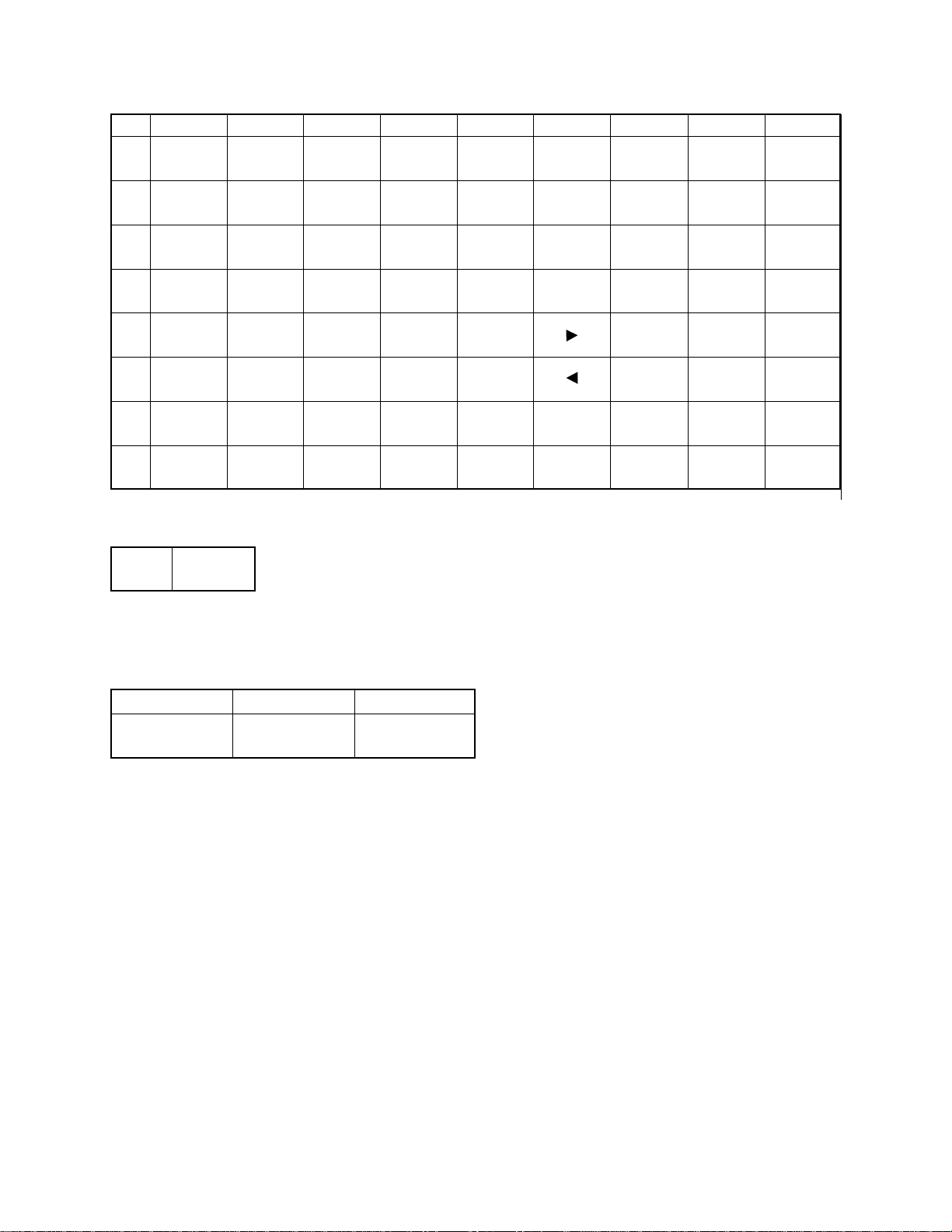
■ To enter diagnostic mode
1. While pressing down “0” and “MODE” buttons, press “POWER” button for turning on.
2. The instrument is set in diagnostic mode and display indicates “Test”.
■ Button check
1. Press “INT/EXT” button.
2. Display indicates “00 Console”.
3. Press buttons in the following order
0 MODE button
1 RECORD button
2 SONG button
3 PATTERN button
4 DSP (digital effect)
button
5 CONTRAST button
6 FREE SESSION
button
7 ONE TOUCH
PRESET button
8 MIXER SELECT
button
9 CHANNEL button
CH1
10
CH2
11
CH3
12
CH4
13
CH5
14
CH6
15
CH7
16
CH8
17
CH9
18
CH10
19
CH11
20
CH12
21
CH13
22
CH14
23
CH15
24
CH16
25
SPLIT button
26
LAYER button
27
RHYTHM button
28
TONE button
29
Number key 7
30
Number key 4
31
Number key 1
32
Number key 0
33
Number key –
34
Number key 2
35
Number key 5
36
Number key 8
37
Number key 9
38
Number key 6
39
Number key 3
40
Number key +
41
DISK button
42
TOUCH RESPONSE
button
43
TUNING/MIDI button
44
SYNTH button
45
DEMO button
46
INTRO button
47
NORMAL/FILL-IN
button
48
VARIATION/FILL-IN
button
49
SYNCHRO/ENDING
button
50
START/STOP button
51
TEMPO button down
52
TEMPO button up
53
BANK button
54
REGISTRATION
buttons A
55
56
57
58
59
60
61
62
63
64
65
66
67
REGISTRATION
buttons B
REGISTRATION
buttons C
REGISTRATION
buttons D
REGISTRATION
buttons E
STORE button
TRANSPOSE button
up
TRANSPOSE button
down
AUTO HARMONIZE
button
ENTER button
Cursor key Left
Cursor key Up
Cursor key Down
Cursor key Right
25
PARAMETER RESET:
MAIN MANU/
CHANNEL VOLUME:
SUB MANU/
CHANNEL SELECT:
28
26
27
789
29
36 37
456
30 35 38
1023
31 34 39
/YESS/NO
32 33 40
DELETE
64
65
66
45
44
43
42
41
67
AMP ENVELOPE
DECAY
SUSTAIN
PITCH ENVELOPE
00 FLAT
01-17 VIBRATO
18-45 OTHERS
4
FULL RANGE
CHORD
FINGERED
CASIO CHORD
1 2 3
MAX
MIN
0
SONG
PATTERN
46 47 48 49 50 51 52 53 54 55 56 57 58 59 61 60 62 63
5
6
7
EXTERNAL
CH 1
CH 2
CH 3
CH 4
CH 5
CH 6
CH 7
CH 8
CH 9
CH 10
CH 11
CH 12
CH 13
CH 14
CH 15
CH 16
INTERNAL
UPPER1
98
UPPER2
LOWER1
LOWER2
ACC VOL.
CHORD1
CHORD2
CHORD3
BASS
RHYTHM
TR1
TR2
TR3
STOREBANK
242322212019181716151413121110
TR4
TR5
TR6
Display shows the button number to be pressed. When the pressed button functions properly, the instr ument emits a verification signal and indicates next button number.
If the button malfunctions, an error alarm sounds and display indicates “Cons ER”.
When wrong button is pressed, the alarm sound is also emitted. In that case, re-press the correct button.
All buttons is pressed correctly, an OK alarm sonds and display indicates "Cons OK".
— 22 —
Page 24

■ Pitch Bender check
1. Press “CH12” button.
2. Display indicates “Bender”.
3. Rotate the pitch bender to the following order
Max → Center → Min → Center
When the pitch bender is proper, an OK alarm sounds and display indicates "OK".
■ AC adaptor detection check.
1. Press “CH14” button.
2. DIsplay indicates "Jack".
3. When the instrument detects that an AC adaptor is plugged in, an OK alarm sounds and indicates
“OK” on the display.
■ Keyboard and pedal check
1. Press “CH10” button.
2. Display indicates “Tch & Pd1”.
In accordance with key, depressions, display indicates velocity value (hexadecimal values 01 to
127), and in accordance with pedal depressions, display indicates "SUS".
■ ROM check
1. Press “CH2” button.
2. Display indicates "ROM", the diagnostic program counts check sums of 1Mbit ROM(inside of CPU)
and 64Mbit ROMs.
3. In accordance with ROMs functions, display indicates;
“ROM H80K” ---------------1Mbit ROM OK
“ROM 64MOK”-------------64Mbit ROMs OK
“ROM H8NG” --------------1Mbit ROM NG
“ROM 64MNG” ------------64Mbit ROMs NG
■ RAM check
1. Press “CH15” button.
2. Display indicates "RAM Test".
3. The program executes write/read test in all the RAM area.
4. When the RAM is proper, display indicates “RAM OK”.
If the RAM malfunctions, “RAM NG” is shown on the display.
— 23 —
Page 25

■ Small sound output
1. Press “CH5” button.
2. The instrument emits a sound in small volume and indicates “sound MIN” on the display.
■ Medium sound output
1. Press “CH6” button.
2. The instrument emits a medium volume sound and indicates “sound MID” on the display.
■ Large sound output
1. Press “CH7” button.
2. The instrument emits a large volume sound and indicates “sound MAX” on the display.
■ Large sound left channel output
1. Press “CH8” button.
2. The instrument emits a large volume sound from the left speaker and indicates “sound L” on the
display.
■ Large sound right channel output
1. Press “CH9” button.
2. The instrument emits a large volume sound from the right channel and indicates “sound R” on the
display.
■ MIDI IN/OUT test
1. Connect MIDI IN and MIDI OUT terminals with a MIDI cable.
2. Press “CH11” button.
3. When the MIDI circuit is normal, display indicates “MIDI OK” whereas “MIDI ER” will be shown if the
MIDI circuit is abnormal.
■ Modulation bender check
1. Press “CH13” button.
2. Display indicates “Modulat”
3. Rotate the modulation bender to the following order.
Max → Min → Max
When the modulation bender is proper, on OK alarm sounds and display indicates “OK”.
— 24 —
Page 26

■ LCD test
1. Press “CURSOR ←” button.
2. Display indicates “LCD Test”.
3. Each pressing of “CURSOR ←” button, displays following patterns in the following order with verification sound.
a. All dots indication
b. No dots indication
c. Checker on 8 character block : pattern A
d. Checker on 8 character block : pattern B
e. Checker on pixel block : pattern A
f. Checker on pixel block : pattern B
g. Displays each pixel (or dot) block in turn + all dots indication
h. Displays each dot in turn + all dots indication
■ LED test
1. Press “CH1” button.
2. Display indicates “LED Test” and LEDs illuminate in the following order with ver ification sound.
a. FULL RANGE CHORD
b. FINGERED
c. CASIO CHORD
d. SONG
e. PATTERN
f. FREE SESSION
g. SYNTH
h. DISK
■ FDD test
1. Press “DISK” button.
2. Display indicates “Dsk0-9E” (which means numeral key 0 to 9 and ENTER button.)
This test executes floppy disk’s write/read test and entering a number selects sectors to be tested.
Larger the number, narrower the check area namely, entering 0 checks all the sectors of the disk.
3. Press “ENTER” button to clean the FDD with cleaning disk. W et type cleaning disk is recommended.
■ To exit from the diagnostic program
Pressing “CURSOR ↓” button sets the instrument in Reset power off state.
If you wish to use the instrument continually after this diagnostic program, perform “System reset” de-
scribed below.
— 25 —
Page 27

<Other utilities>
■ System reset
1. While pressing down “ENTER” button, turn power on.
2. Display indicates “Reset?”.
3. Pressing “+” button initializes the instrument.
Pressing “–” button invalidates system reset.
4. The instrument turns on automatically.
■ Touch off max
1. While pressing down “RHYTHM” and “MODE” buttons, turn the power on.
2. Display indicates “TouchMax”.
3. The instrument is set in touch off max mode.
In this state, sound volume in touch response off mode becomes maximum.
— 26 —
Page 28

FDD ERROR MESSAGE
Error Message Reason of Error
Rea
For
Dis
Dis
dOn l
ma t
kR/W
kFul l
Mem
No t
No
S
Disk
y
Ful l
SMF0
The file being written to is read-only.
The disk format is not one supported by this keyboard.
Error occurred during reading from the disk.
Disk is full.
Not enough memory to perform the process.
No memory is available to load data.
An attempt was made to play data that is not SMF
FORMAT 0.
An attempt was made to access a disk while no disk
is loaded in the drive.
No
Pro
Con
Wr o
File
tect
ver t
g
n
Da t
There is no file that corresponds to the file that was
specified.
A save or delete operation was attempted with a
disk that is write protected.
The attempted file conversion was not successful.
Something is wrong with the data you are trying to
load.
— 27 —
Page 29

1
MAJOR W A VEFORMS
3
2
5
6
1 Clock signal for CPU
Check point CP1
2 Clock signal for DSP
LSI3 pin 14
5 NMI signal
LSI9 pin 64
6 Reset signal RESB
LSI9 pin 87
4
7
8
3 Voltage VDD
IC5 pin 2
4 Reset signal RES
IC5 pin 1
7 Sound signal L-OUT
SIELD-WIRE PE-W
8 Sound signal L-VOL0OUT
JJ connector pin 1
Tone:
Grand Piano (No. 000), Volume: Max.
Touch speed: Max., Key: A4
9
0
9 Key common signal KC0
JA connector pin 11
0 Key common signal KC1
JA connector pin 12
— 28 —
Page 30

Main PCB JCM733-MA1M
6
1
PRINTED CIRCUIT BOARD
5
4
3
9 10
T op View
2
Bottom View
— 29 —
Page 31

Sub PCB JCM733-MA2M
7
Sub PCB JCM733-MA3M
T op View
8
T op View
— 30 —
Page 32

Console PCBs JCM733-CN1M
Console PCBs JCM733-CN2M
T op View
T op View
— 31 —
Page 33

Display PCB JCM733-LCD1M
T op View
Bottom View
— 32 —
Page 34

Keyboard PCBs JCM763T-KY1M
T op View
Keyboard PCBs JCM763T-KY2M
T op View
— 33 —
Page 35

41
30
29
33
34
35
36
37
31
32
38
40
40
39
4
7
9
8
3
28
1
43
23
27
42
26
26
23
27
22
46
44
45
50
47
48
50
49
49
11
12
20
21
19
25
6
10
R-1
24
5
R-2
R-5
R-4
R-5
R-3
18
16
17
14
13
15
2
EXPLODED VIEW
— 34 —
Page 36

PARTS LIST
WK-1800
Notes: This parts list does not include the cosmetic parts, which
parts are marked with item No. "R-X" in the exploded
view.
Contact our spare parts department if you need these
parts for refurbish.
1. Prices and specifications are subject to change without prior notice.
2. As for spare parts order and supply, refer to the
"GUIDEBOOK for Spare parts Supply", published
seperately.
3. The numbers in item column correspond to the same
numbers in drawing.
— 35 —
Page 37
PARTS PRICE LIST
R - Rank
WK-1800
N Item Code No. Part Name Specification Q Price Code R Remarks
MA1M PCB
N 1 10023172 PCB ASSY/MA1M TK-M241341*1(M733) 1 EI A
N BT1 38150679 BATTERY/LITHIUM CR2032/1HF1 1 AG X
D3 23901820 DIODE 1SS355TE-17 1 AA C
N D4 79114127 DIODE RB520S-30TE61 1 AA C
IC1,IC6 21054543 IC/LMOS TC7W32F(TE12L) 2 AC C
IC2 21052821 IC/LMOS TC7S04F(TE85R) 1 AC C
IC301,302 21056083 IC/LMOS TC7WU04F(TE12L) 2 AD C
IC4 21010642 IC/CMOS TC74HC08AF(TP1) 1 AC C
IC5 20121883 IC/CMOS RN5VD40AA-TR 1 AE C
N LSI1 10014314 LSI LHMN5KPP 1 BG B
LSI2 10014313 LSI LHMN5KPN 1 BG B
LSI3 20117434 LSI HG51B155FD 1 BU B
LSI4 20125572 LSI TC55257DFL-70L(EL) 1 AS B
LSI5 21056665 LSI UPD63200GS-E1 1 AX B
LSI6 20125987 LSI TC190C020AF-001 1 BC B
LSI7 20126186 LSI TC551001CF-70L(EL) 1 BK B
LSI8 20126186 LSI TC551001CF-70L(EL) 1 BK B
N LSI9 10014312 LSI HD6433048SA89F 1 CB B
LSI10 20109990 LSI HD63266F 1 BT B
Q1 22521169 TRANSISTOR 2SC4081T106S 1 AA C
N X1 10025033 OSCILLATOR/CERAMIC CSTCV16.00MXJ2C3-T 1 AD C
X2 25902788 OSCILATOR/CRYSTAL AT-49-24.576MHZ 1 AS C
MA2M PCB
N 2 10023173 PCB ASSY/MA2,3M TK-M241342*1(M733) 1 DK B
D202,D204,D212
D215,D218
D203,D211 23901463 DIODE/SCHOTTKY SB20-03B 2 AD C
D205,D206 23901344 DIODE 1SS133T-77-T 2 AA C
N D209,D210 10025045 DIODE/ZENER MTZJT-777.5B 2 AA C
D213 23601085 DIODE/ZENER HZS6B1L-TD 1 AA C
N D214 10025044 DIODE/ZENER MTZJT-776.2A 1 AA C
D216 23902828 DIODE/SCHOTTKY RB441Q-40T-77 1 AA C
N IC201 10022651 IC/MONOLITHIC LA4663 1 AV C
IC202 21130084 IC/MONOLITHIC BA9700A 1 AK C
IC203 21141421 PHOTO COUPLER PC900V 1 AK C
IC204 21051092 IC/CMOS TC74HC04AP 1 AC C
IC205 21210072 IC/MONOLITHIC NJM2068DD 1 AD C
IC206,IC207 21210072 IC/MONOLITHIC NJM2068DD 2 AD C
J201 35015012 JACK/DC HEC2305-01-920 1 AC C
J202,J203 36120584 JACK YKB21-5012 2 AD C
J204 36120789 JACK YKB21-5010 1 AC C
J205 35014816 JACK/DIN YKF51-5051 1 AH C
J206 36120665 JACK/PHONE YKB21-5006 1 AG C
N Q201,Q212-Q215 22501627 TRANSISTOR 2SC1740STPS 5 AA C
Q203 22501627 TRANSISTOR 2SC1740STPS 1 AA C
N Q205,Q206 10025042 TRANSISTOR 2SD1468STPR 2 AA C
Q207 22521253 TRANSISTOR 2SB1566F 1 AC C
N Q208,Q211 10025037 TRANSISTOR 2SA933STPS 2 AA C
Q209 22510672 TRANSISTOR 2SB1548-P.CS 1 AD C
N 3 10023177 PCB ASSY/LCD1M TK-M241343*1(M733) 1 CS B
N 4 10014320 LCD LD-B10608E 1 BZ C
N 5 10025053 CONNECTOR M441032-1 2 AR C
N 6 10025056 PACKING M441122-1 2 AB X
N 7 10025057 PC-FILM M441031-1 1 AE X
N 8 10021742 REFLECTOR M141035-1 1 AM X
23901344 DIODE 1SS133T-77-T 5 AA C
BL ass'y
Notes : Q - Quantity per unit
- 36 -
Page 38

N Item Code No. Part Name Specification Q Price Code R Remarks
R - Rank
N 9 10014316 CFL HMBV4BG2W182NLU AZG 1 AX B
10 69273420 HOLDER/RUBBER M440758-1 2 AA X
LSI601 2012 6018 LSI SED1278F2A 1 AV B
Q601,Q602 2253 0710 TRANSISTOR 2SD965-R(TA) 2 AB C
N T601 10025034 TRANSISTOR TE-CFL733-1M1 1 BB C
CN1 ~ CN2 PCBs
N 11 10023168 PCB ASSY/CN1M TK-M241344*1(M732) 1 CI B
N 12 10023171 PCB ASSY/CN2M TK-M341305*1(M732) 1 BY B
D402-D469 23901344 DIODE 1SS133T-77 68 AA C
IC401,IC402 21051239 IC/CMOS TC74HC164AP 2 AH C
LED401,LED402
N
LED405,LED408
LED403,LED406
N
LED407,LED409
N LED404 10022654 LED SLZ-181B-22-AB-T2 1 AB C
13 69222720 KEY SET/LT WHITE M312118*1 5 AP B
14 69237900 KEY SET/LT76R WHITE M340231*1 1 AO B
15 69237910 KEY SET/LT76L WHITE M340230*1 1 AO B
16 69068482 KEY SET/LS BLACK M140369B-3 2 AJ B
N 17 10025058 KEY SET/LSK-8P BLACK M140369-8 1 AH B
N 18 10025059 KEY SET/LSK-3P BLACK M140369-7 1 AN B
N 19 10025055 RUBBER/CONTACT CB M241297-1 5 AJ B
N 20 10025054 RUBBER/CONTACT EB M241298-1 1 AH B
N 21 10025060 RUBBER/CONTACT CG M241299-1 1 AH B
N 22 10023178 PCB ASSY/KY1,2M TK-M241345*1(M732) 1 CO B
N 23 10025062 PORT/SPEAKER M241300-1 2 AD X
N 24 10025077 BND-ASS'Y TK-M340804*4(M732) 1 BV C Bender
N 25 10025078 BND-ASS'Y TK-M340804*5(M732) 1 BU C Modulation
26 38311105 SPEAKER S12J96A 2 BM C Woofer
27 38311106 SPEAKER S05JH48A 2 AT C Twitter
28 69215030 KNOB/SLIDE M311859-1 2 AA C
29 69269280 RUBBER/BUTTON M240800-1 1 AU C
N 30 10025052 RUBBER/BUTTON M240801-2 1 AC C
31 69269310 RUBBER/BUTTON M240803-1 1 AU C
32 69269320 RUBBER/BUTTON M240804-1 1 AU C
N 33 10019019 RUBBER/BUTTON M241285-1 1 AF C
34 10019021 RUBBER/BUTTON M241286-1 1 AF C
N 35 10019022 RUBBER/BUTTON M241289-1 1 AC C
N 36 10019023 RUBBER/BUTTON M241290-1 1 AC C
N 37 10019025 RUBBER/BUTTON M241291-1 1 AC C
N 38 10019026 RUBBER/BUTTON M241292-1 1 AC C
39 69259380 RUBBER/BUTTON M240641-1 1 AB C
40 69259410 RUBBER/BUTTON M240640-1 4 AB C
N 41 10025049 PLATE/DISPLAY M341269-1 1 AD C
N 42 10025069 COVER/BATTERY M341288*1 1 AV C
43 35022318 CONNECTOR/LITHIUM BATT. MLES-A60-T 1 AA X
44 10151485 FDD DF354H064C 1 CW B
N 45 10025048 BLACKET L/FDD M341272-1 1 AD X
N 46 10025046 BLACKET R/FDD M341273-1 1 AD X
N 47 10014321 CABLE/FDD YAF11-0892 1 AT X
N 48 10025064 2P CONNECTOR AMP-2P-105-M733 1 AF X
49 69269420 RUBBER/DAMPER M440598-2 4 AB X
50 69269431 SPACER M440597A-1 4 AC X
N 10034272 STAND/MUSIC M140744-2 1 AI X
N 10034273 FLOPPY DISK WK1800FD-1 1 AV X
10022652 LED SLZ-281B-22-T2 4 AA C
10022653 LED SLZ-281B-13-T1 4 AA C
Keyboard
Panel
Accessory
Notes : Q - Quantity per unit
- 37 -
Page 39

MainPCB JCM733-MA1M
ROM1 ROM2
SCHEMATIC DIAGRAMS
6
5
Working RAM
DSP
CPU
D/A
Converter
Key Controller
3
Reset IC
2
RAM2
RAM1
1
4
FDD
Controloer
Backup Power
— 38 —
109
Page 40

SubPCB JCM733-MA2M/MA3M
Power Amp.
Regulator IC
7
8
— 39 —
Page 41

Console PCBs JCM733-CN1M/CN2M
S-Register
S-Register
— 40 —
Page 42
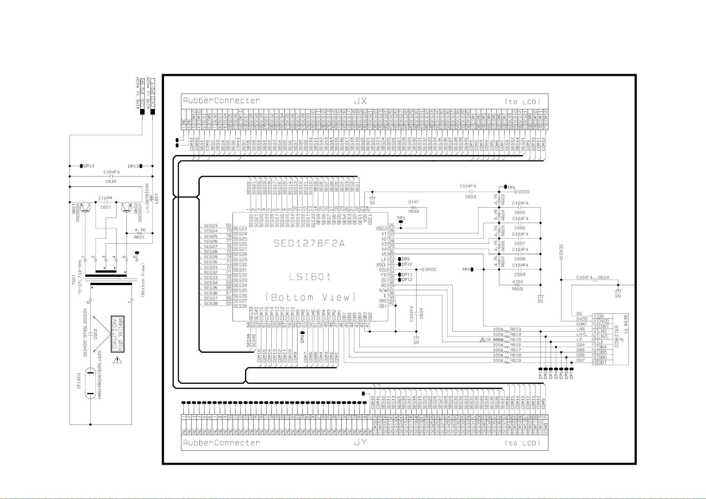
LCD Driver PCB JCM733-LCD1M
Back Light Circuit
LCD Driver
— 41 —
Page 43

Keyboard PCBs JCM763T-KY1M/KY2M
— 42 —
Page 44

Ver.1 : Apr. 2007
• Correction of the CIRCUIT DESCRIPTION (P6)
CASIO COMPUTER CO.,LTD.
Overseas Service Division
6-2, Hon-machi 1-Chome
Shibuya-ku, Tokyo 151-8543, Japan
 Loading...