

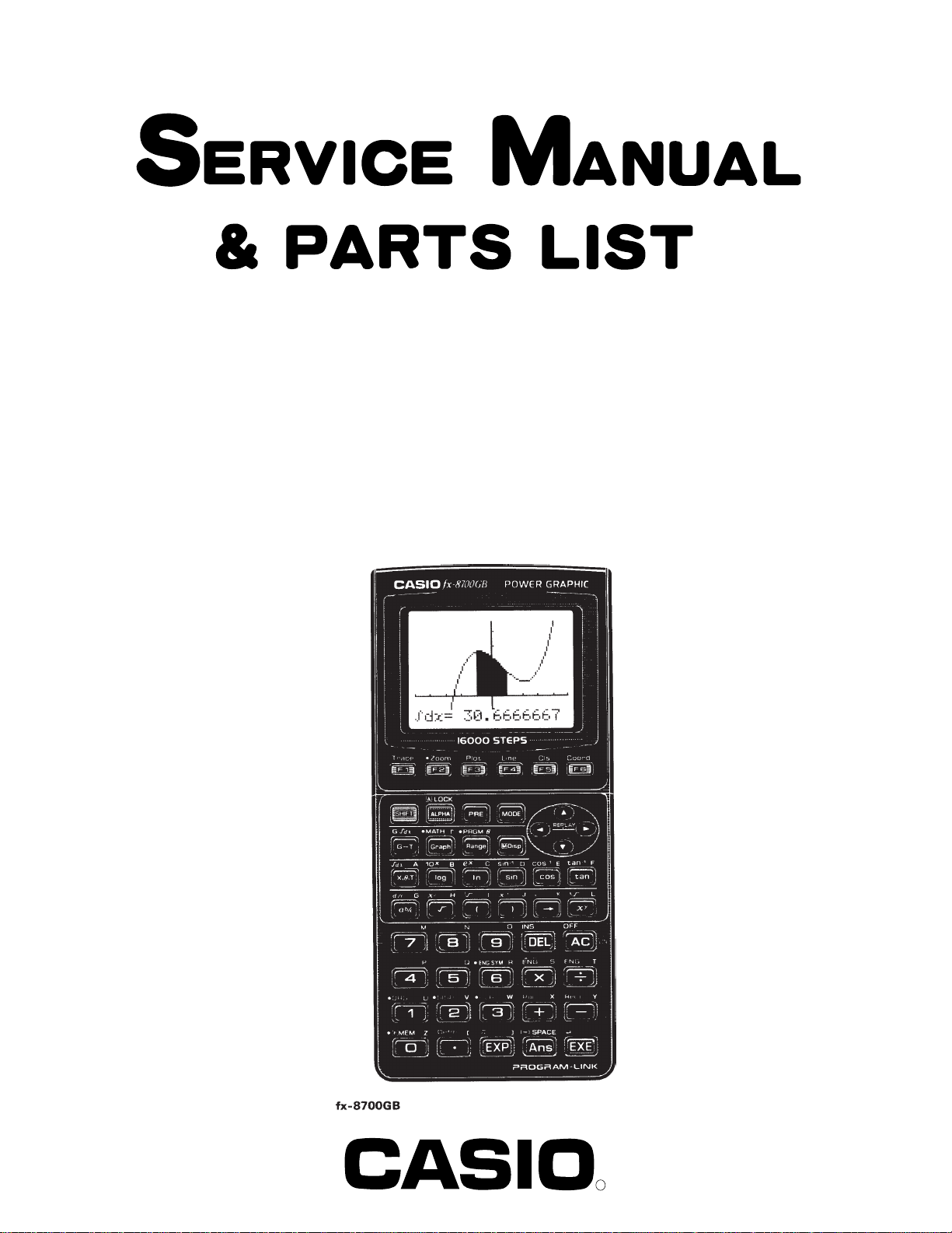
Page 1
fx-8700GB(LX-388)
INDEX
JUN. 1992
(without price)
R
Page 2

CONTENTS
1. SCHEMATIC DIAGRAM ................................................................................... 3
2. SPECIFICATIONS............................................................................................. 4
3. PIN FUNCTION ................................................................................................. 5
4. TROUBLESHOOTING ...................................................................................... 9
5. OPERATION CHECK...................................................................................... 10
6. DATA TRANSFER CHECK............................................................................. 16
7. EXPLODED VIEW ........................................................................................... 17
8. PCB VIEW ....................................................................................................... 18
9. PARTS LIST .................................................................................................... 21
Page 3
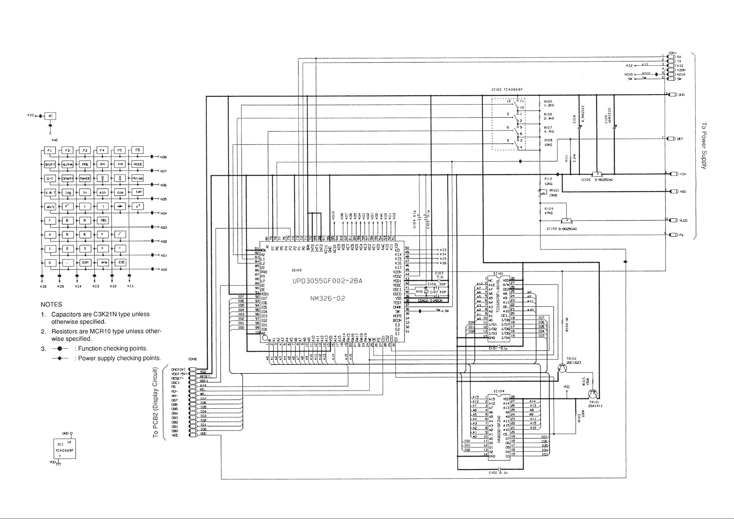
1. SCHEMATIC DIAGRAM
1-1. Main Block
— 1 —
Page 4
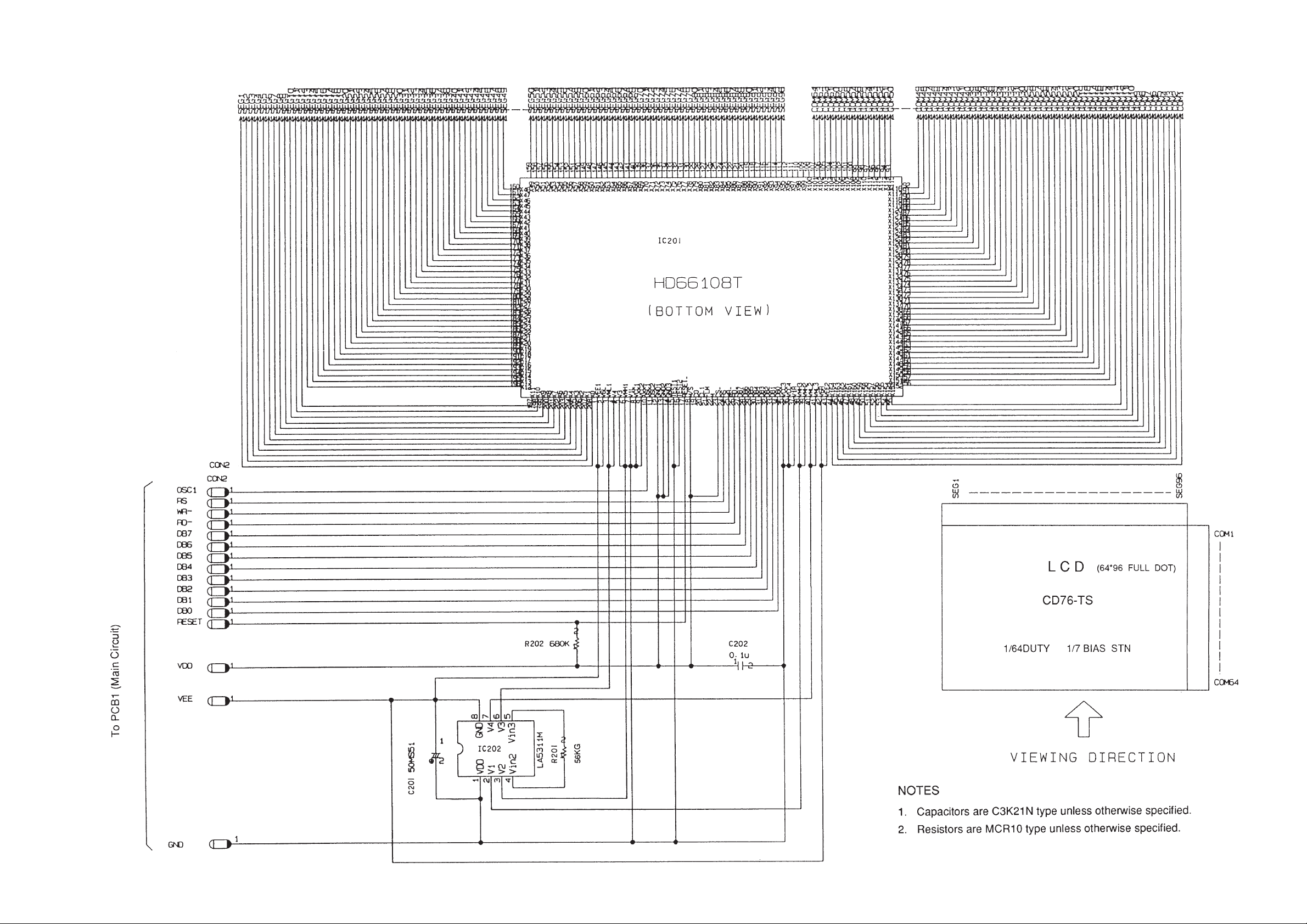
1-2. Display Block
— 2 —
Page 5
1-3. Power Block
— 3 —
Page 6

2. SPECIFICATIONS
Program communication functions
RS-232C INTERFACE;
Communication method: Start-stop (Asynchronous)
Transmission speed (baud): 1200 2400 4800 9600BPS
Parity bit: EVEN ODD NONE
Bit length: 8 bit
Stop bit
Transmit: 1 bit
Receive: 2 bit
General
Display system: Liquid crystal display, 10-digit mantissa plus 2-digit exponent.
16 characters by 8 lines (96 by 64 dots).
Power supply: Main — 3 lithium batteries (CR2032)
Memory protection — 1 lithium battery (CR2032)
Power consumption: 0.22W
Battery life: Main — Approximately 100 hours on CR2032
*The battery will also discharge in approximately one year if the unit is left with the power
switched off.
Memory protection — Approximately 1 year
*Note that the life of the battery that comes with the unit starts when the battery is loaded in
the unit at the factory. The life you get from a battery may be shorter than normal because
of the time the unit spends in transport, on the shelf, etc.
*Leaving dead batteries in the unit for a long time can result in demage to the unit. Replace
batteries as soon as possible after they get weak or go dead.
Auto power off: Power is automatically switched off approximately 6 minutes after last operation.
Ambient temperature range: 0°C ~ 40°C (32°F ~ 104°F)
Dimensions: 15.6mmH × 81mmW × 172.5mmD (5/8"H × 33/4"W × 63/4"D)
Weight: 179g (6.3oz) including batteries
— 4 —
Page 7
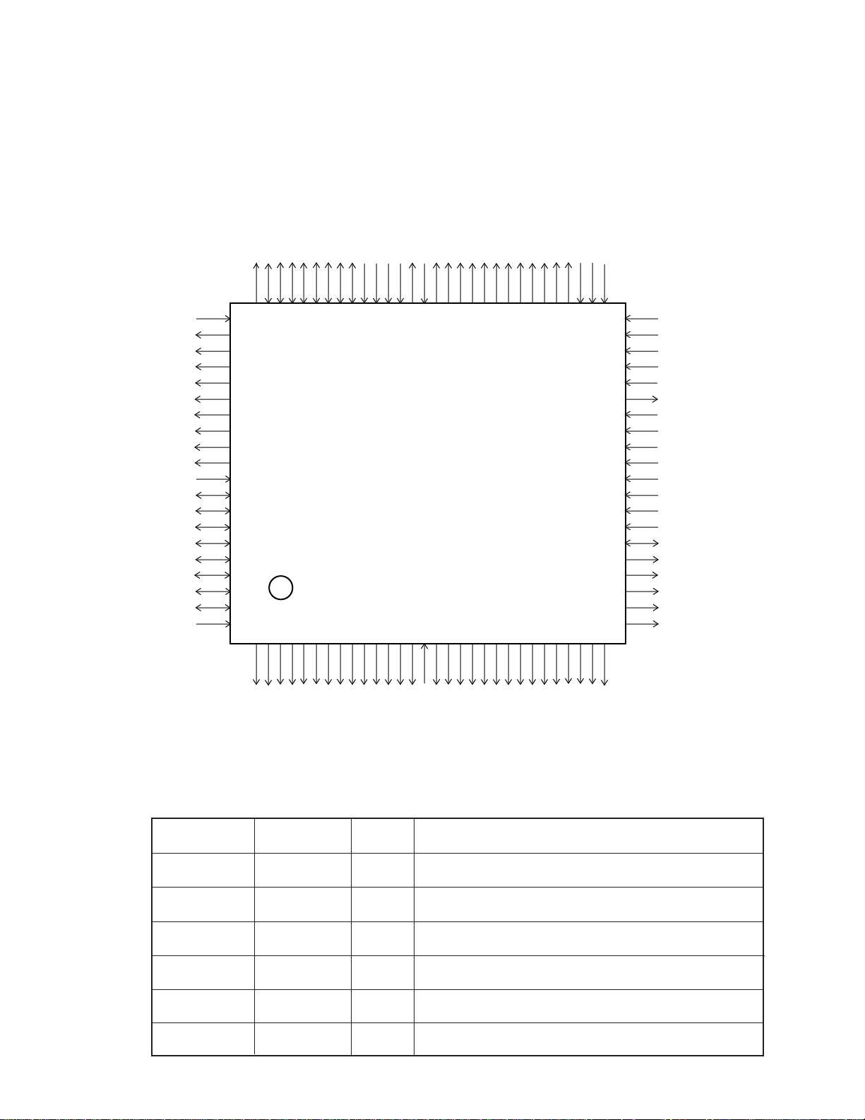
3. PIN FUNCTION
1. CPU (µPD3055GF002-2BA) (IC105)
WENL
H2
DT
PRO
FR
LP
GC
DE
VDD1
IO7
IO6
IO5
IO4
IO3
IO2
IO1
IO0
VSS
H1P7P6P5P4P3P2P1P0
8079787776757473727170696867666564636261605958575655545352
L1
L2
100 99 98 97 96 95 94 93 92 91 90 89 88 87 86 85 84 83 82 81
123456789
BRK
INT0
INT1
INT2
KC11
GND
KC10
KC9
KC8
KC7
KC6
KC5
KC4
KC3
KC2
KC1
KC0
KA0
KI0
KI1
101112131415161718192021222324252627282930
KI2
51
31 32 33 34 35 36 37 38 39 40 41 42 43 44 45 46 47 48 49 50
KI3
KI4
KI5
KI6
KI7
V2ON
VDD2
VDD1
VOSC
OSCI
OSCO
VSS
TEST
ONMK
SW
MDP2
BCON
E3
E2
E1
A0A1A2A3A4A5A6A7A8
A9
A10
A11
A12
A13
VSS
A14
A15
RA14
RA15
RA16
RA17
RA18
RA19
WE
OE
Pin No. Signal IN/OUT Function
1~14, 16, 19, 20
A0~A16 OUT Address bus
15, 39, 100 VSS IN GND (-5V)
24 WE OUT Write enable signal
25 OE OUT Output enable signal
27, 29 CS1, CS3 OUT Chip select signal
30 E0 OUT Chip enable signal
— 5 —
FE
CS1
CS2
CS3
EO
Page 8
Pin No. Signal IN/OUT Function
36 SW IN/OUT Switch signal
37 ONMK IN Voltage detect signal terminal
38 TEST IN Test terminal
40, 41 OSCO/I IN Clock terminal
42 VOSC IN Power supply for clock
43, 91 VDD1 IN Power supply (0V)
44 VDD2 IN Power supply
45 V2ON OUT Power on signal
46~53 KI0~KI7 IN Key input signal
54 KAC OUT On key scan signal
55~63, 65
KC0~KC8, KC10
OUT Key scan signal
66 GND IN GND (-5V)
68, 70 INT0, INT2 IN (0V)
69 INT1 IN Interrupt terminal
71 BRK IN (0V)
72~79 P0~P7 IN/OUT IO port terminal
P0 : Data transfer terminal (Output)
P1 : Data transfer terminal (Input)
P6 : Voltage detect signal terminal (Input)
80, 82 H1, H2 OUT Output port (Low active)
81 WENL IN GND (-5V)
83, 84 L1, L2 OUT Output port (High active)
89 GC OUT Not used
92~99 IO0~IO7 IN/OUT Data bus
— 6 —
Page 9

2. RAM (TC55257BFL-8510L) (IC101)
1
2
3
4
5
6
7
8
9
10
11
12
13
14
NC
A12
A7
A6
A5
A4
A3
A2
A1
A0
I/O1
I/O2
I/O3
GND
VDD
R/W
CE2
A8
A9
A11
OE
A10
CE1
I/O8
I/O7
I/O6
I/O5
I/O4
28
27
26
25
24
23
22
21
20
19
18
17
16
15
TC55257BFL-8510L
Pin No. Signal IN/OUT Function
2~10, 21, 23~25
11~13, 15~19 IO1~IO8 IN/OUT Data bus
1 Not used
14 GND IN GND (-5V)
20 CE1 IN Chip enable
22 OE IN Output enable
26 CE2 IN Chip enable
27 R/W IN Read/Write terminal Low : Data input
28 VDD IN Power supply (0V)
A0~A12 IN Address bus
— 7 —
High: Data output
Page 10
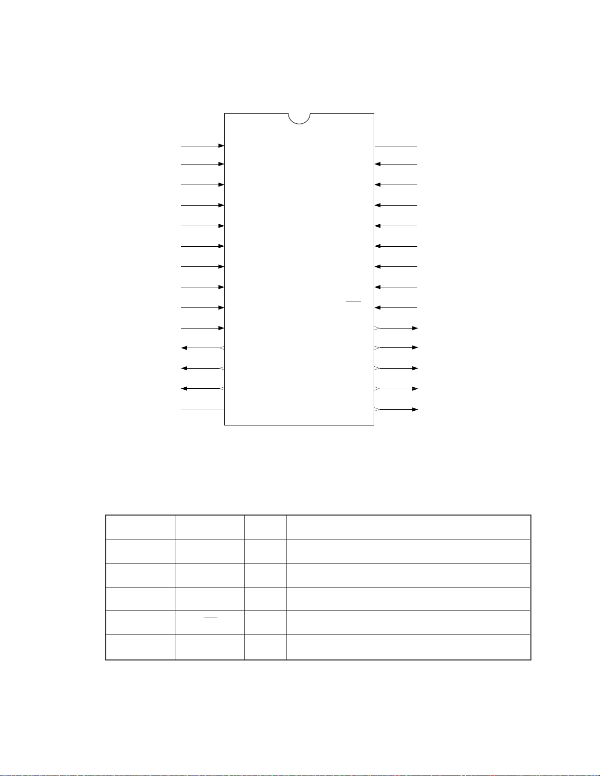
3. ROM (HN62321 BFZ40) (IC104)
10
11
12
13
14
1
2
3
4
5
6
7
8
9
A15
A12
A7
A6
A5
A4
A3
A2
A1
VDD
A14
A13
A8
A9
A11
A15
A10
CE
HN62321BFZ40
A0
O0
O1
O2
GND
O7
O6
O5
O4
O3
28
27
26
25
24
23
22
21
20
19
18
17
16
15
Pin No. Signal IN/OUT Function
1~10, 21, 23~27
11~13, 15~19 O0~O7 OUT Data bus
14 GND IN GND (-5V)
20 CE IN Chip enable
28 VDD IN Power supply (0V)
A0~A15 IN Address bus
— 8 —
Page 11

4. TROUBLESHOOTING
SYMPTOM CAUSE SOLUTION
Intermittent display Dirt or poor contact on battery Clean or adjust pressure
of contact
Poor contact on power switch Clean or replace power
switch
Poor connection on PC joiner Resolder or replace
Poor soldering on LSI, capacitor, or resistor Resolder
No display at all Weak battery Replace battery
Dirt or poor contact on battery Clean or adjust pressure
of contact
Poor contact on power switch Clean or replace power
switch
Poor connection on PC joiner Resolder or replace
Defective LSI, capacitor, or resistor Replace
Erratic display Poor contact between LCD and PCB Replace the heat seal
Poor soldering on LSI Resolder or replace
display PCB ass'y
Certain key does not Dirt on key contact Clean or replace contact
function
Heavy key motion Clean or replace the key
Poor soldering on LSI Resolder
Defective LSI, capacitor, or resistor Replace
All keys do not function Constant contact is made on a certain key Separate the contact
Defective LSI, capacitor, or resistor Replace
Heavy key motion Dirt or scratch on the key Clean or replace the key
— 9 —
Page 12

5. OPERATION CHECK
NO. OPERATION DISPLAY NOTE
Turn the slide switch (LOCK)
on and push the "RESET" button
1
F1
2
RUN / COMP
G-type : REC/CON
angle : Deg
display : Nrm1
YES RESET ALL NO
RUN / COMP
G-type : REC/CON
angle : Deg
display : Nrm1
✽ ✽ RESET ALL ✽ ✽
SHIFT AC
3
While pushing F6 and
ab/c , push AC
4
No display
= = Lx 388 TEST = =
1. LCD 4. ROM
2. KEY 5. TRS
3. RAM 0. rst
— 10 —
Page 13

NO. OPERATION DISPLAY NOTE
1
5
EXE
6
EXE Reverse
No display
Checker
display
checker
display
7
EXE
8
— 11 —
All dots display
Page 14

NO. OPERATION DISPLAY NOTE
EXE
9
10
EXE
2
Frame
= = Lx 388 TEST = =
1. LCD 4. ROM
2. KEY 5. TRS
3. RAM 0. rst
Trace
11
12
Trace
F1
Zoom
— 12 —
Page 15

NO. OPERATION DISPLAY NOTE
Zoom
F2
13
Push each key sequentially
as it appears on the display
(Plot, Line, Cls, Coord,
SHIFT, and so on)
14
Plot
15
16
Ans
EXE
EXE
= = Lx 388 TEST = =
1. LCD 4. ROM
2. KEY 5. TRS
3. RAM 0. rst
— 13 —
Page 16

NO. OPERATION DISPLAY NOTE
3
17
(After a few seconds)
18
. . .
< < RAM OK > >
OK
< < RAM NG > > NG
19
20
EXE
4
= = Lx 388 TEST = =
1. LCD 4. ROM
2. KEY 5. TRS
3. RAM 0. rst
. . .
— 14 —
Page 17

NO. OPERATION DISPLAY NOTE
(After a few seconds)
21
EXE
22
0 1 1 2 D 1 2 E
= = Lx 388 TEST = =
1. LCD 4. ROM
2. KEY 5. TRS
3. RAM 0. rst
Check the
number.
If the number
is different,
there is
something
wrong in
ROM or the
circuit.
23
24
0
SHIFT AC
RUN / COMP
G-type : REC/CON
angle : Deg
display : Nrm1
✽ ✽ RESET ALL ✽ ✽
END
No display
— 15 —
Page 18

6. DATA TRANSFER CHECK
* Turn off both units and connect them using the appropriate cable.
NO.
Master Slave
Function Display Function Display
1
2
While
pushing
F6 and
ab/c,
push AC
5
= = Lx 388 TEST = =
1. LCD 4. ROM
2. KEY 5. TRS
3. RAM 0. rst
TRANSMIT CHECK
1.
COM CHECK
2. RANDOM DATA
While
pushing
F6 and
ab/c,
push AC
5
= = Lx 388 TEST = =
1. LCD 4. ROM
2. KEY 5. TRS
3. RAM 0. rst
TRANSMIT CHECK
1.
COM CHECK
2. RANDOM DATA
OUT
3
111. TRANS
4
5
1
2. RECEIVE
1. TRANS
2. RECEIVE
1. TRANS
2. RECEIVE
2
1. TRANS
2. RECEIVE
DATA RECEIVE
TO STOP
DATA RECEIVE
TO STOP
OUT
PRESS AC KEY
PRESS AC KEY
6 (OK) RECEIVE OKTRANSMITTED
(OK)
(NG)
TRANSMIT ERROR
(or)
1. TRANS
2. RECEIVE
EXE
= = Lx 388 TEST = =
or
1. LCD 4. ROM
(AC : NG)
2. KEY 5. TRS
3. RAM 0. rst
0 0
RUN / COMP
G-type : REC/CON
angle : Deg
display : Nrm1
✽ ✽ RESET ALL ✽ ✽
(NG)
EXE
or
(AC : NG)
RECEIVE NG
= = Lx 388 TEST = =
1. LCD 4. ROM
2. KEY 5. TRS
3. RAM 0. rst
RUN / COMP
G-type : REC/CON
angle : Deg
display : Nrm1
✽ ✽ RESET ALL ✽ ✽
— 16 —
Page 19

7. EXPLODED VIEW
— 17 —
Page 20

8. PCB VIEW
1. Main Block
— 18 —
Page 21

2. Display Block (PCB L387-4)
— 19 —
Page 22

3. Power Block (PCB L387-2)
— 20 —
Page 23

8. PARTS LIST
— 21 —
Page 24

— 22 —
Page 25

— 23 —
Page 26

8-11-10, Nishi-Shinjuku
Shinjuku-ku, Tokyo 160, Japan
Telephone: 03-3347-4926
 Loading...