

Page 1
R
INDEX
CTK-100
(with price)
CTK-100
ELECTRONIC KEYBOARD
Page 2

CONTENTS
SPECIFICATIONS.......................................................................................................... 1
BLOCK DIAGRAM ......................................................................................................... 2
CIRCUIT DESCRIPTION ................................................................................................ 3
TROUBLESHOOTING.................................................................................................... 5
IC AND TRANSISTOR LEAD IDENTIFICATIONS ........................................................ 6
SCHEMATIC DIAGRAMS .............................................................................................. 7
PCB VIEW & MAJOR WAVEFORMS............................................................................ 8
EXPLODED VIEW ........................................................................................................ 10
PARTS LIST ................................................................................................................. 11
Page 3

SPECIFICATIONS
General
Number of Keys: 49
Polyphonic: 8-note
Preset Tones: 100
Auto-Rhythms: 100
Auto-Accompaniment: CASIO Chord/Fingered
Demonstration Tune: Classical Medley
Built-In Speakers: 10 cm dia. 1.0W Input Rating: 2 pcs.
Terminals: Output Jack [Output Impedance: 120 Ω, Output Voltage: 3 V (rms)MAX],
AC Adapter Jack (DC 9 V)
Power Source: 3-way AC or DC source
AC: AC adapter AD-5
DC: 6 AA size dry batteries
Battery life: Approx. 3 hours (SUM-3/R6P)
Approx. 6 hours (AM-3/LR6)
Power Consumption: 5.0 W
Dimentions: 86 x 857 x 285 mm (HWD)
(3-3/8 x 33-3/4 x 11-1/4 inches) (HWD)
Weight: 3.2 kg (7.0 lbs) excluding batteries
Standard Accessory: Music stand
Electrical
Current Drain with 9V DC:
No Sound Output 47 mA ± 20%
Maximum Volume 413 mA ± 20%
with keys C2, D2, E2 and F2 pressed in
Car-Horn tone, Volume; Maximum
Output Level (Vrms with 8 Ω load each channel): 76 mV ± 20%
with key G2 pressed in Street Organ tone
Speaker Input Level: 935 mV ± 20%
with key G2 pressed in Street Organ tone
Minimum Operating Voltage: 6.0 V
— 1 —
Page 4
— 2 —
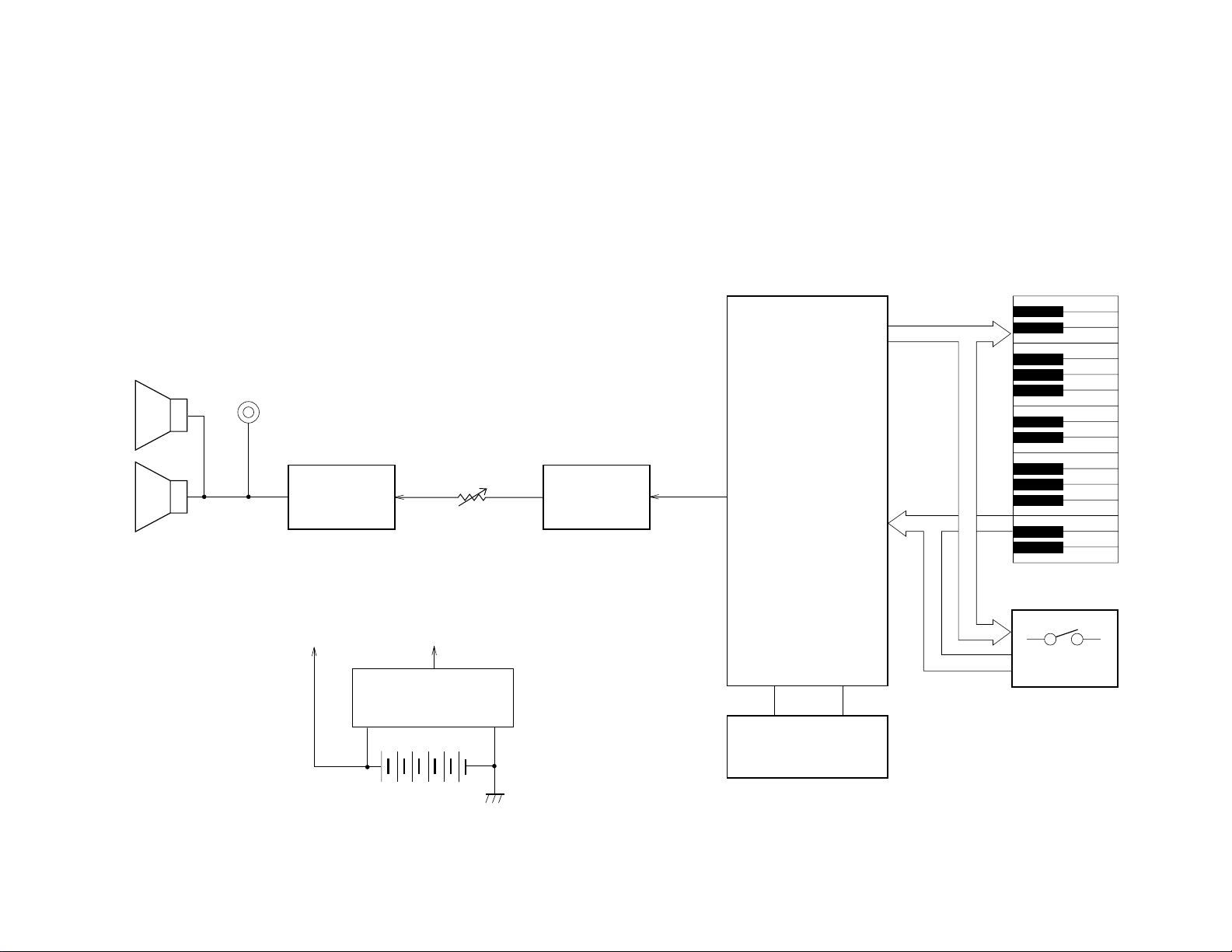
Speakers
Output Jack
Amplifier
LA4598
Main Volume
BLOCK DIAGRAM
Filter
T3/T4
KO0~KO9
CPU
MSM6387-13
KI0~KI7
VC +9V
VDD +5V
Power supply circuit
T2
Keyboard
Switches
Oscillator
Page 5
Key and Switch Matrix
0IK1IK2IK3IK4IK5IK6IK7IK
CIRCUIT DESCRIPTION
0OK
)1CK(
1OK
)2CK(
2OK
)3CK(
3OK
)4CK(
4OK
)5CK(
5OK
)6CK(
6OK
)7CK(
7OK
)8CK(
8OK
)9CK(
01 2C2#C2D2#D2E2F
23 2#F2G2#G2A2#A2B
45 3C3#C3D3#D3E3F
67 3#F3G3#G3A3#A3B
89 4C4#C4D4#D4E4F
enoTmhtyhR4#F4G4#G4A4#A4B
opmeT
pU
/tratS
potS
omeD6C
9OK
opmeT
nwoD
5C5#C5D5#D5E5F
nI-lliF5#F5G5#G5A5#A5B
.pmoccA
1emuloV
)niM(
rewoP
FFO
.pmoccA
2emuloV
.pmoccA
3emuloV
lamroNderegniF
.pmoccA
4emuloV
)xaM(
OISAC
drohC
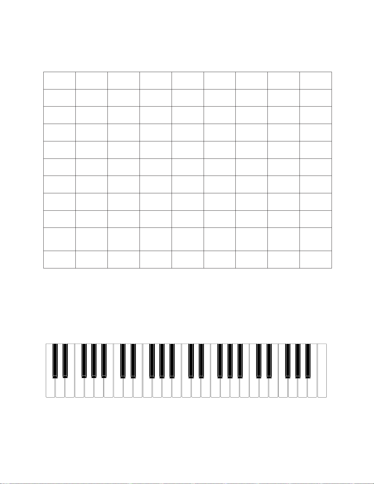
Nomenclature of Keys
C#2
D#2
C2
D2
E2
F2
G2
A2
C#3A#2G#2F#2
D#3
B2 C3 D3 E3
F#3 G#3 A#3 C#4 D#4 F#4 G#4 A#4 C#5 D#5 F#5 G#5 A#5
F3 G3 A3 B3 C4 D4 E4 F4 G4 A4 B4
— 3 —
C5 D5 E5 F5 G5 A5 B5
C6
Page 6

CPU (MSM6387-13)
The CPU contains a sound data ROM and a DAC (Digital to Analog Convertor), and it provides a sound
waveform in accordance with the pressed key and the selected tone.
The following table shows the pin functions of the CPU.
Pin No. Terminal In/ Out Function
1, 2 TEST1, TEST2 Not used. Connected to ground.
Power ON reset terminal. When the power switch is
3 RESET In
turned on, the terminal receives a low level signal and
the internal circuits of the LSI are initialized.
4 AVDD In +5 V sorce for the built-in DAC
5 OUT Out Sound waveform output
6 AGND In Ground (0 V) source for the built-in DAC
7 GND In Ground (0 V) source
8, 9 COSI, COSO In/Out 21.725 MHz clock pulse input/output
10 VDD In +5 V source
11 ~ 18 KI0 ~ KI7 In Input terminal from keys and switches
19, 20 KO11, KO10 Not used.
21 ~ 30 KO9 ~ KO0 Out Key and switch scan signal output
Filter Block
Since the sound signal from the CPU is a stepped waveform, the filter block is added to smooth the
waveform.
VDD
T3
120K
C273(H) C473(H)
T4
3.3K
2SC1740SQ
1K
C822(H)
AG
AG
C333(H)
1K
2.2K
From CPU
C823(H)
AG
To main volume
2SC1740SQ
1K
AG AG
150K
1.5K
— 4 —
Page 7

Power Amplifier (LA4598)
The power amplifier is a 2-channel power amplifier with a standby switch.
The following table shows the pin functions of the power amplifier.
Pin No. Terminal In/Out Functiion
1 Power GND Ground (0 V) source
2 Ch1 B.S. Out Terminal for a bootstrap capacitor
3 Ch1 OUT In Channel1 output
4 VCC In +9 V source. Connected to the power source directly.
5 Ch1 N.F. In Negative feedback input
6 Ch1 IN In Channel1 input
7 D.C. Terminal for a decoupling capacitor
8 Pre GND In Ground (0 V) source
9 Standby In Power control signal input. 0 V: OFF, +9 V: ON
10 Ch2 IN In Channel2 input
11 Ch2 N.F. In Negative feedback input
12 Ch2 OUT Out Channel2 output
13 Ch2 B.S. Terminal for a bootstrap capacitor
14 NC Not used.
TROUBLESHOOTING
Nature of Trouble Faulty Block Checkpoint
No power Power Supply Circuit Emitter of T2 should provide +5.5 V.
Base of T2 should receive +6 V.
Power Jack Jack contact.
No sound at all Power Amp. (LA4598) Pin 9 should receive +9 V when the
power switch is turned on.
Check output signals of pins 3 and 12.
CPU (MSM6387-13) Pins 21 ~ 30 should provide pulses.
Pin 5 should have a sound signal when
keys are pressed.
Oscillator Pins 8 and 9 of the CPU should receive
an ocsillation signal.
A certain key or switch
does not function
Certain keys or switches
do not function
Key and Switch Matrix Dust on the contact.
Key and Switch Matrix Open circuit on KC or KI line.
— 5 —
Page 8

IC AND TRANSISTOR LEAD IDENTIFICATION
MSM6387-13
30292824272625
KO0
KO1
KO2
KO3
KO4
TEST2
TEST1
RESET
AVDD
OUT
1
2
374
5
23222120191817
KO6
KO5
KO7
KO8
KO9
GND
AGND
COSI
COSO
VDD
6
8
9
1011121314
LA4598
12345678910111213
KO10
KO11
KI0
KI1
KI7
KI2
KI6
KI3
16
KI5
KI4
15
VCC
Ch1 B.S.
Ch1 OUT
Power GND
D.C.
Ch1 IN
Ch1 N.F.
Ch2 IN
Standby
Pre GND
Ch2 N.F.
Ch2 B.S.
Ch2 OUT
T3, T4: 2SC1740SQ T2: 2SD2008Q,R
BCE
C
E
B
— 6 —
Page 9

Keyboard PCBs M496K-KY1M, KY2M
SCHEMATIC DIAGRAMS
— 7 —
Page 10

PCB VIEW and MAJOR WAVEFORMS
5671432
— 8 —
Page 11

Main PCB M4502-MA1M
4.6
2.0
7
1.4
4.6
4
2.4
0.0
7.5
4.3
8.7
1.2
0.0
8.4
0.0
8.4
0.0
1.2
4.3
7.5
1.7
1
1
5.5
6.18.7
5
6
2
0.0
0.0
0.3
0.0
0.3
0.0
0.0
0.0
5.1
4.2
2.3
0.0
0.0
2.4
4.6
5.0
0.0
3
0.2
0.2
0.2
0.2
0.2
0.2
0.2
0.2
0.2
0.2
— 9 —
Page 12

EXPLODED VIEW
— 10 —
Page 13

PARTS LIST
CTK-100
Notes: 1. Prices and specifications are subject to change with-
out prior notice.
2. As for spare parts order and supply, refer to the
"GUIDEBOOK for Spare parts Supply", published
separately.
3. The numbers in item column correspond to the same
numbers in drawing.
Page 14

FOB Japan
N Item Code No. Parts Name Specification QM N.R.Yen R *
Unit Price
PCB Ass'y M5505-MA1M
2011 2961LSI MSM6387-13 1 1 580 A F
2114 2891IC LA4598 1 1 140 A B
2220 1387Transistor 2SC1740SQ-TP-T 210 13 A A
2253 0357Transistor 2SD2008Q,R-T105-T 110 30 A A
2310 7848Zener diode RD4.3ESB2-T1-T 120 12 A A
2360 0035Zener diode RD6.2ESB2-T1-T 110 10 B A
2370 0343LED LN28RPX-(TT) 120 16 C A
2390 1323Diode RB100A-T32-T 120 29 B A
2390 1344Diode 1SS133T-77-T 1520 3 C A
2590 0742Ceramic oscillator EFO-GC2175C3 1 5 64 B B
2606 1141Carbon film resistor R-20-1K-J-T23-T 2520 2 C A
2606 1155Carbon film resistor R-20-330-J-T23-T 220 2 C A
2606 1169Carbon film resistor R-20-100-J-T23-T 320 2 C A
2606 1183Carbon film resistor R-20-10K-J-T23-T 120 2 C A
2606 1204Carbon film resistor R-20-3.3-J-T23-T 220 2 C A
2606 1274Carbon film resistor R-20-1.5K-J-T23-T 220 2 C A
2606 1288Carbon film resistor R-20-2.2K-J-T23-T 120 2 C A
2606 1295Carbon film resistor R-20-2.7K-J-T23-T 120 2 C A
2606 1309Carbon film resistor R-20-470-J-T23-T 120 2 C A
2606 1358Carbon film resistor R-20-3.3K-J-T23-T 120 2 C A
2606 1449Carbon film resistor R-20-150K-J-T23-T 120 2 C A
2606 1484Carbon film resistor R-20-820-J-T23-T 120 2 C A
2606 1498Carbon film resistor R-20-1.8K-J-T23-T 120 2 C A
2606 1554Carbon film resistor R-20-120K-J-T23-T 120 2 C A
2606 1617Carbon film resistor R-20-120-J-T23-T 220 2 C A
N 2606 1708Carbon film resistor R-20-47-J-T23-T 120 2 C A
2801 7910Electrolytic capacitor 16RE3-470-T2-T 210 27 C A
2805 3061Electrolytic capacitor 6.3RE2-220-T2-T 110 26 C A
2805 3142Electrolytic capacitor 16RE2-10-T2-T 120 14 C A
2807 0926Electrolytic capacitor 10RE2-470-T2-T 310 36 C A
2807 1023Electrolytic capacitor 50RE2-1-T2-T 120 15 C A
2807 1091Electrolytic capacitor 6.3RE2-100-T2-T 320 18 C A
2807 1112Electrolytic capacitor 10RE2-100-T2-T 320 12 C A
2807 1139Electrolytic capacitor 50RE2-R47-T2-T 120 12 C A
2813 0658Semiconductive capacitor RT-C50TKYR822K-T 120 6 C A
2813 1925Semiconductive capacitor RT-B70TKYR333K-T 120 8 C A
2813 1939Semiconductive capacitor RT-B70TKYR473K-T 120 9 C A
2813 1953Semiconductive capacitor RT-B90TKYR823K-T 220 8 C A
2813 3101Semiconductive capacitor RT-B70TKYR273K-T 120 6 C A
2813 3283Ceramic capacitor UP050F104Z-A-B 220 8 C A
2819 5443Module capacitor CNB8X471M 1 5 51 C B
2830 6229Mylar capacitor AMZV-104K50-T 210 13 C A
2845 3220Ferrite beads EXC-ELDR35V-T 520 12 C A
3501 7049DC jack HEC2305-01-330 110 29 A A
3612 0711Miniature jack YKB21-5101 1 5 90 B B
3665 0217Terminal B CT-00160D 110 26 C A
3841 0539Inductor ELE-V100KR-T 420 26 C A
3841 0910Coil FL5R1R0PNA 210 39 C A
N 3841 0959Inductor ELE-R100KR-T 410 25 C A
N 4317 4271Blank PCB M4502-MA1M M111795A-1 1 1 230 C C
6921 6200Battery spring 700 (+) M412124-1 120 17 B A
6921 6211Battery spring 700B (-) M412171A-1 120 12 B A
6921 8570Felt 280X18 M412199-1 110 26 C A
N 6922 4700PCB ass'y M4502-MA1M M111796*1 1 1 1700 B P
Notes: N– New parts
M– Minimum order/supply quantity
R– Rank
— 11 —
Page 15

FOB Japan
N Item Code No. Parts Name Specification QM N.R.Yen R *
Unit Price
PCB Ass'y Keyboard
2301 0101Diode 1S2473-T-77-T 4920 8 C A
JX 3725 2030PC joiner MASKX JSF50-9-140 110 34 C A
JA 3725 2401PC joiner M283A JSF50-15-240M 1 5 91 C B
4317 1610Blank PCB M496K-KY1M M110799-1 1 1 120 C B
4317 1621Blank PCB M496K-KY2M M210939A-1 1 5 53 C B
N 6918 5500Keyboard PCB ass'y M110798*2 1 1 950 C J
Mechanical Parts
1 6920 5572SL knob 238 M311360B-1 310 14 B A
N 2 6922 4780Panel 502 M111763-1 1 1 810 C I
3 6909 5890SL contact 12D CSB-12D 310 35 B A
N 4 6922 3980Rubber button 700 M211536-2 1 1 140 B B
N 5 6922 5750Felt 502A M412333-1 120 10 C A
N 6908 6160Felt 156G M43073-1 120 7 C A
N 6 3831 0665Speaker 10G42AFA 2 1 200 B C
7 6917 4474White key set CEGB M110589D-1 4 1 120 A B
8 6917 4484White key set DFAS M110590D-1 1 1 110 A B
9 6917 4494White key set DFA M110591D-1 3 1 170 A B
10 6917 4506Black key set 10P M110594F-1 2 1 130 A B
N 11 6922 4790Case sub ass'y M211760*1 1 1 1500 C O
11-1 6917 8462Key damper 49 M411202B-1 1 5 33 C A
11-2 6918 2020key stopper 4500 M411303-1 1 5 58 C B
N 11-3 6921 9990Key stopper M700 M412235-1 1 5 56 C B
N 6921 9470Felt 10X225 M411280-2 320 13 C A
12 6917 4453TAC31 M110603C-1 1 1 190 B C
13 6917 4463TAC18 M110605C-1 1 1 110 B B
14 6910 1130Sponge A M4630-1 120 14 C A
N 15 6921 6231Joiner cover M412126A-1 110 24 C A
16 6921 6220Bottom plate M311898-1 1 1 200 C C
N 17 6906 7092Battery cover sub ass'y M311200B*12 1 5 37 B A
Screws
18 0009 2682Screw 2.6 x 8 1050 2 C A
19 0009 4589Screw 2.6 x 8 850 2 C A
20 0009 4588Screw 2.6 x 18 1450 2 C A
21 0008 6417Screw 4 x 10 1450 2 C A
22 6918 1992Screw M411279B-1 1850 2 C A
23 0009 2680Screw 4 x 8 1250 2 C A
Accessory
6916 7880Music stand M310827-1 1 1 120 C B
Notes: N– New parts
M– Minimum order/supply quantity
R– Rank
— 12 —
Page 16

MA0300941A
 Loading...