

Page 1
SERVICE MANUAL
INDEX
(without price)
ELECTRONIC CASH REGISTER
CE-6800 (EX-475EP)
MAY. 2001
Printer Model : M-U420B-031
Page 2

CONTENTS
CE-6800 Page
1. SPECIFICATIONS........................................................................................ 1
2. BLOCK DIAGRAM....................................................................................... 3
3. TO OPEN THE UPPER CASE ..................................................................... 5
4. CIRCUIT EXPLANATION ............................................................................ 7
4-1. Power supply circuit ................................................................................................. 7
4-2. Reset and power down circuit.................................................................................. 8
4-3. CPU description......................................................................................................... 8
4-4. Momory chip selection circuit................................................................................ 11
4-5. Flash ROM1 address circuit ................................................................................... 12
4-6. Memory map ............................................................................................................ 12
4-7. Printer drive circuit.................................................................................................. 13
4-8. RS232C port COM1 circuit...................................................................................... 14
4-9. RS232C port COM2 and COM3 circuit ................................................................... 15
4-10. To mount optional circuit ....................................................................................... 16
5. DIAGNOSTIC OPERATION....................................................................... 17
5-1. To start the diagnostic program ............................................................................ 17
5-2. Check item ............................................................................................................... 17
5-3. Operation of each test............................................................................................. 17
5-4. Switch status test .................................................................................................... 18
5-5. Individual function test ........................................................................................... 19
5-6. To exit the diagnostic mode ................................................................................... 27
6. IC DATA ..................................................................................................... 28
7. PCB LAYOUT ............................................................................................ 38
8. CIRCUIT DIAGRAM ................................................................................... 40
9. PARTS LIST............................................................................................... 56
Page 3
1. SPECIFICATIONS (CE-6800)
1-1. Electrical specifications
• Power consumption In operation Max. 0.7 A
Power OFF 0.3 A
• Memory protection Back-up battery VL3032/1F2
Back-up period 90 days (25 °C)
Battery life Replace the battery every 5 years.
Recharge time 48 hours
• Clock & Calendar Accuracy Within ± 30 sec. per month (25 °C)
Auto calendar Effective until 2099 A.D.
1-2. Environmental specifications
• Operating temperature 0 °C ~ 40 °C
• Operating humidity 10 % ~ 90 %
• Storage temperature -25 °C ~ 65 °C
110V
Min. 0.3 A
• Storage humidity 10 % ~ 95 %
• Vibration strength 1.5 G (The machine must be in the carton box)
1-3. Main components
• CPU Name uPD784215GC201-8EU
• RAM1 and 2 Name HY628100ALLG-70
• Option RAM3 and 4 Name HM628512BLP-5/7SCL
• Flash ROM Name LH28F016SCT-L95
• Printer Name M-U420-031
• Roll paper Type Fine-quality paper
Number of control bit 8bit
Internal RAM 4 KBytes
Capacity 1 Mbits
Capacity 512 Kbytes
Capacity 16 M bits
Print method Impact dot matrix printer
Paper cut Manual paper cut
Size Width 44.5 ± 0.5 mm
Roll diam 83 mm or less
Thickness 75 ± 15 µm
— 1 —
Page 4
1-4. Drawer List
DRAWER NAME Specification NOTE
• DL-2771 D-9A2C-B84-9*
1-5. Option List
DEVICE NAME MODEL NOTE
• RAM CHIP RAM-610-10LL Capacity 4Mbits (512 Kbytes)
• Wet cover WT-77
• Modem Sports star Recommend model : U.S.Robotics
• P/C cable PRL-CB-2 Com 1 port only
• Handy scanner HHS-15 Com 2 port only
• Fixed scanner HS1250 Com 2 port only (PSC model)
• Laser scanner Quick Scan 6000 Com 2 port only (PSC model)
• Slip printer SP-1300 Connect to Com 2 or 3.
56.4Kbps Com 1 port only
It is possible to drive only one printer.
• External printer UP-350 Connect to Com 1,2 or 3.
It is possible to drive until 2 printers.
• External printer UP-250 Connect to Com 1,2 or 3.
It is possible to drive until 2 printers.
• Scale Model 6710 Com 3 only (NCI model)
• Slip printer cable PRT-CB-8C Connect Com 2 or 3. (Cable lngth 1.5m)
• External printer cable PRT-CB-8A Connect to Com 1,2 or 3. (Cable length 3 m)
• External printer cable PRT-CB-8B Connect to Com 1,2 or 3. (Cable length 5 m)
• Power unit PS-170 Epson model
for External printer
• Power cord AC-170 Epson model
for power unit
• Power-board JDC model
• Molti-drow kit MDL-10
• ARCNET board IO-PB-14 In-line communication board
CAUTION
Danger of explosion if battery is incorrectly
replaced.
Replace only with the same or equivalent type
recommended by the manufacturer.
Dispose of used batteries according
to the manufacture’s instructions.
— 2 —
Page 5
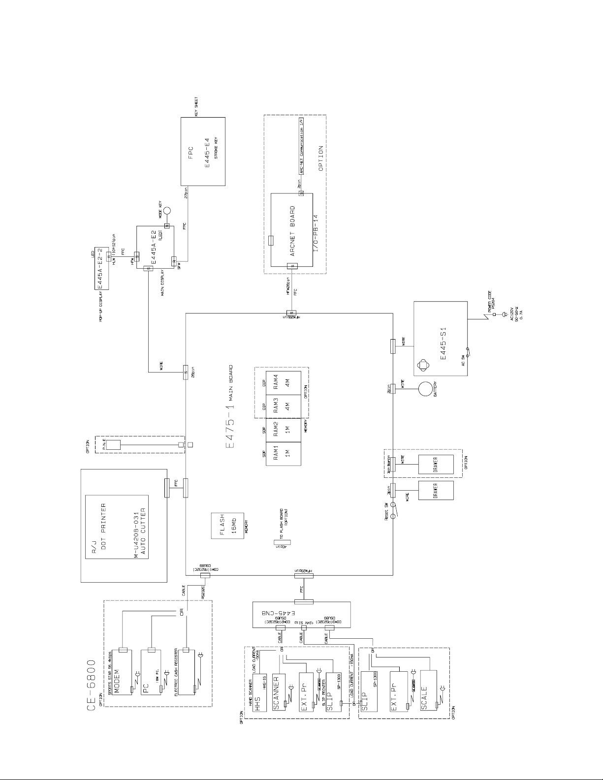
2. BLOCK DIAGRAM
2-1. PCB CONNECTION
— 3 —
Page 6
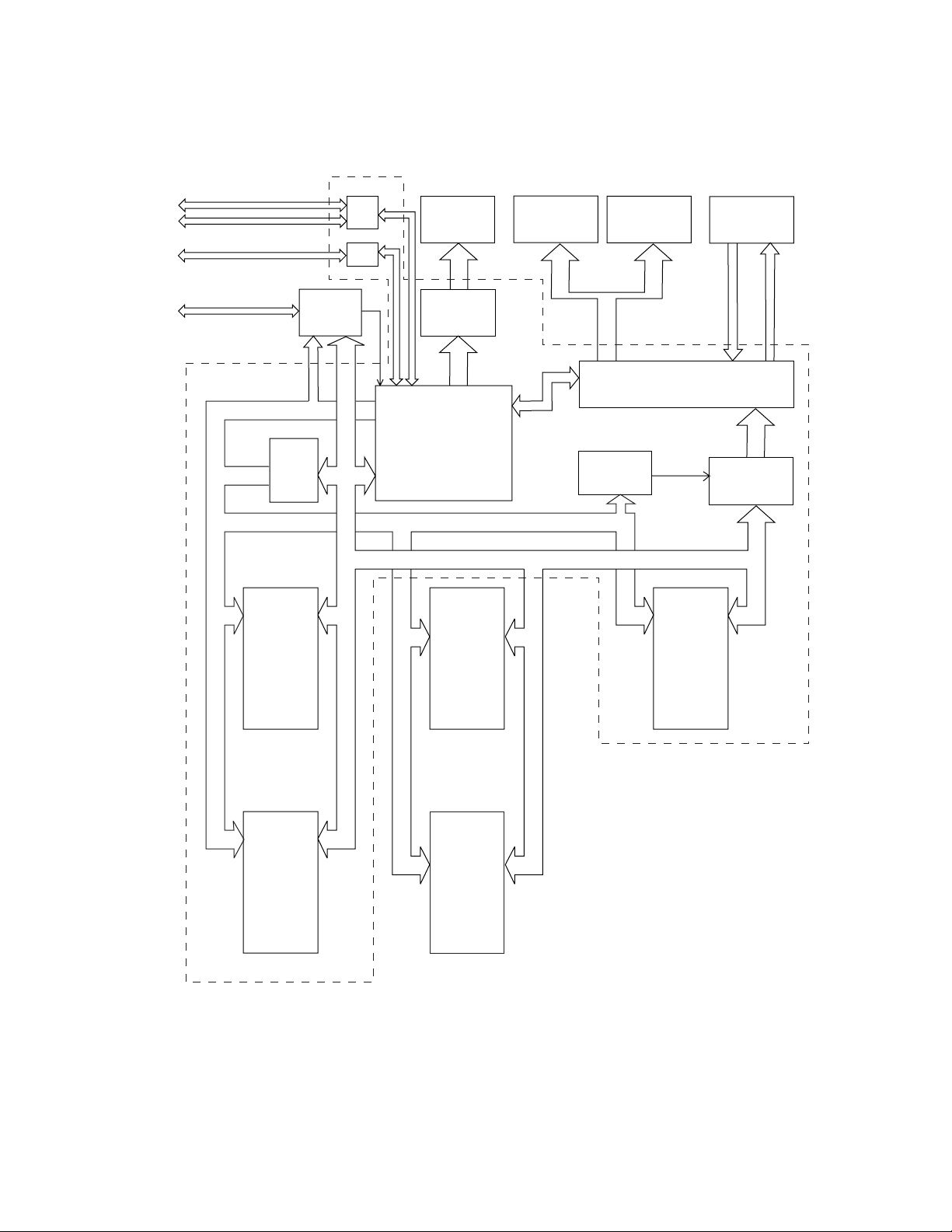
2-2. BLOCK DIAGRAM (CE-6800)
COM3
COM2
COM1
IN-Line
ARCNET
driver
Option I/O PB14
Address bus A8 - A19
Address
Latch
A0 -A7
RAM1
HY628100A
LLG-70
(128 K bytes)
Driver
Driver
CPU
uPD784215GC201-8EU
Data bus D0 -D7
Printer
M-U420-031
Printer driver
RAM3
(Option)
HM628512ALP-7
512 K bytes
(RAM-610)
Main display
(Dot & segment)
Customer
Keyboard
display
Display driver and Key control circuit
I/O selector
Flash ROM 1
LH28F016SCT-L95
Data buffer
(2 M bytes)
RAM2
HY628100A
LLG-70
(128 K bytes)
MAIN PCB E457-1 C
RAM4
(Option)
HM628512ALP-7
512 K bytes
(RAM-610)
— 4 —
Page 7
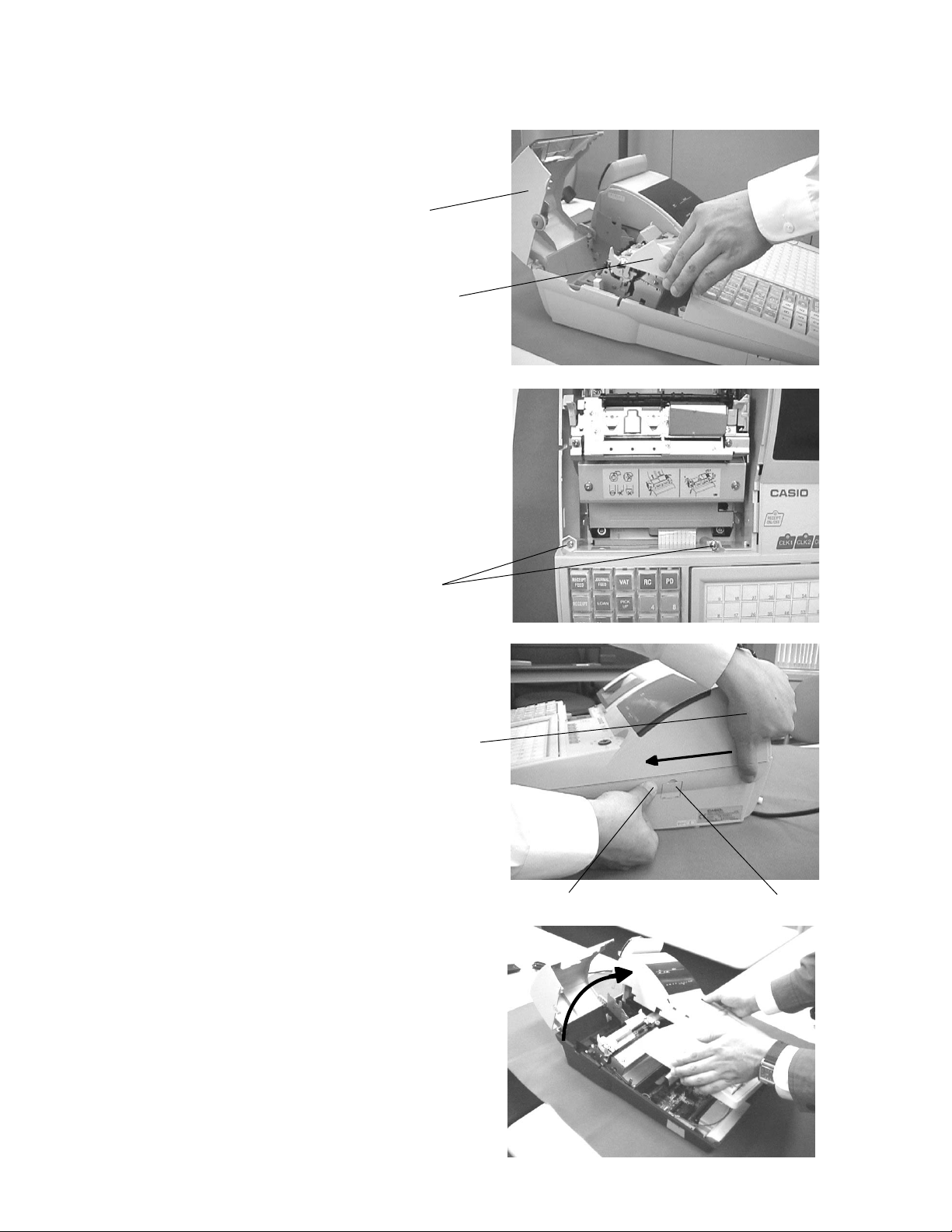
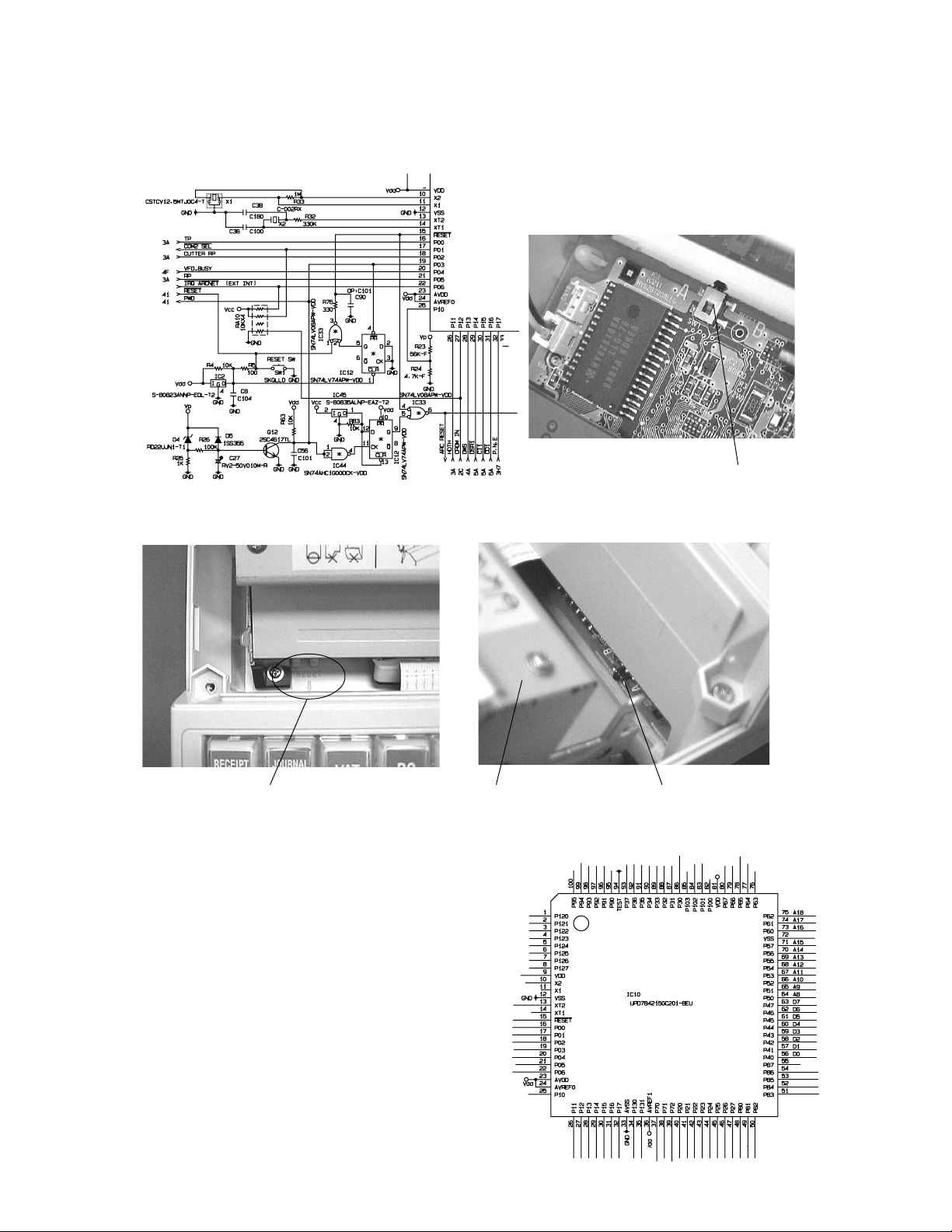
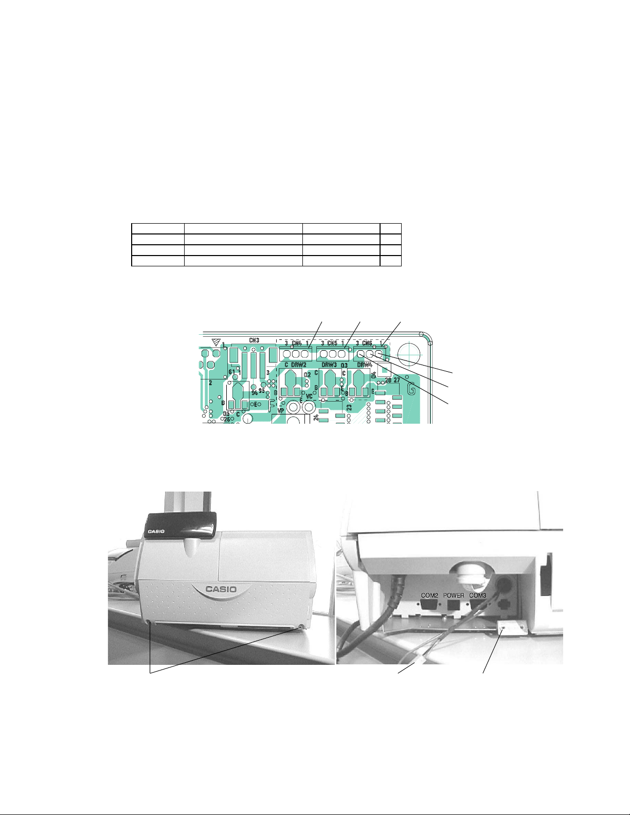
3. TO OPEN THE UPPER CASE
1. Open the printer cover. Then, remove the ribbon
cover from the machine.
Open the printer cover.
Remove the ribbon cover.
2. Remove the 2 screws of the upper case.
Remove the 2 screws.
3. Push the 3 dots marking point at the right side of
lower case. At the same time, slide the upper case
to the front side.
Slide the upper case
to the front side.
4. Open upper cese from the left side.
Press the 3 dots marking point.
Power switch cover
— 5 —
Page 8
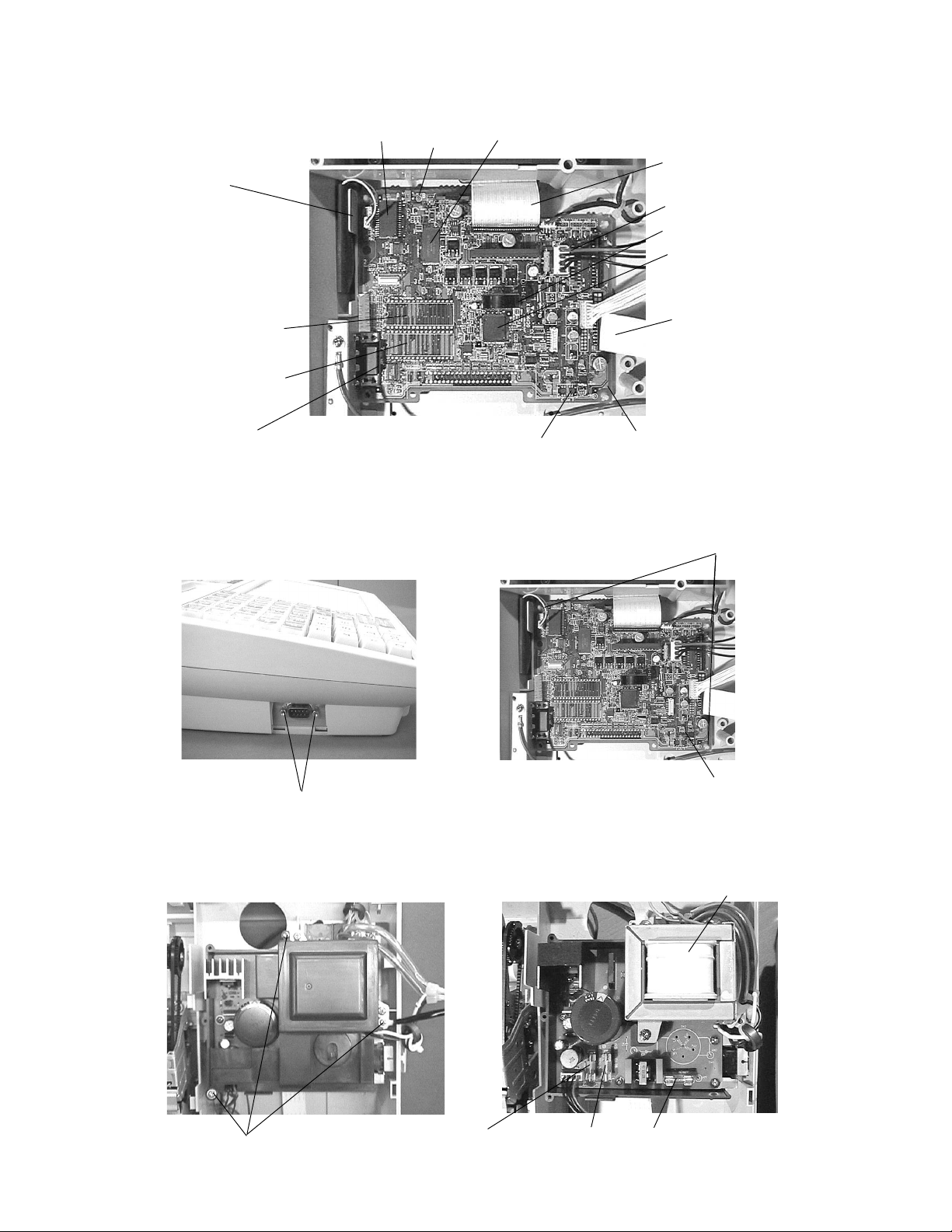
5. The each parts of the Main PCB are located as shown in the picture.
Flash ROM 1 (2 Mbytes)
Keyboard select switch
Printer cable
Power supply connector
Buzzer
CPU
Display cable
Main PCB
Battery
COM 1 port
RAM 4
Option
RAM 3
Option
RAM 1 (128 Kbytes)
Reset Switch
6. To remove the Main PCB, release the 3 locking supporters of point A and the COM1 port outside screws.
Point A
Release 3 locking
suppeares.
Main PCB
Remove 2 screws for COM 1 port.
7. Power supply unit cover is removed by 3 screws. And, the 3 Fuses are located as shown in the picture.
Power transformer
Remove the 3 screws.
Then, remove the power supply cover.
Fuse F3
250V 400mA
(Not used for CE-6000)
— 6 —
Fuse F2
250V 2A
Fuse F1
250V 1A
Page 9
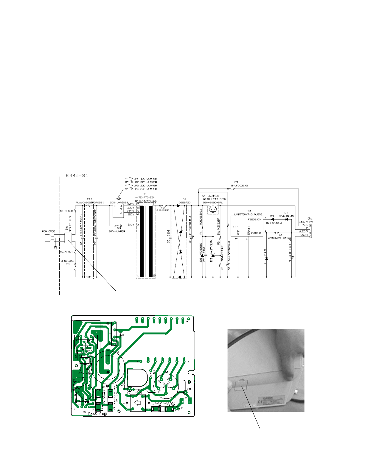
4. CIRCUIT EXPLANATION
4-1. Power supply circuit
The power supply circuit provides the following voltage for the main circuit.
Output Pin No1----- VC1 (DC32.3V): To the VC line for the VFD Display power. (Not used for CE-6000)
Output Pin No.2---- VC2 (DC24V): To the Vp line for the printer power.
Output Pin No.3---- VLED (DC5.85V): To the Vcc,Vcc2 and Vdd for the logic circuit power.
Output Pin No.4---- GND: Signal GND.
The power switch SW1 is located at the right side of the lowercase.
After connected the power plug into AC outlet and turn on the SW1, the transformer T1 will genarate the
about AC33V to secondary side. Then, after rectifier circut, the VC1 (DC32.3V) is supplied to the VC line
for display power (for the drive of display tube. Not for LED model.)
The IC2 is the shunt regulator for the control of Q1 transistor. This circuit is genarate the VC2 (DC24V)
for the printer power. The IC1 is regulator for 5V power supply.
Power switch SW1
Power supply PCB E445-S1
Power SW1 cover
— 7 —
Page 10
4-2. Reset and powe down circuit
The rest and power down circuit are as following circuit. The reset switch is provided for the hard reset
to cleare the system error. Use this switch only when the FMAC or MAC are not possible to perform.
Reset switch
The position of Reset switch
From top of view From rear of view
The mark of reset switch
Printer
4-3. CPU pin description(uPD784215GC201-8EU)
The CPU pin descriptions are as follows:
— 8 —
Reset switch
Page 11
CPU pin description(uPD784215GC201-8EU)
Pin No. Signal Name Description In/Out
1 P120 HD1 HEAD PIN DRIVE HD1 Out
2 P121 HD2 HEAD PIN DRIVE HD2 Out
3 P122 HD3 HEAD PIN DRIVE HD3 Out
4 P123 HD4 HEAD PIN DRIVE HD4 Out
5 P124 HD5 HEAD PIN DRIVE HD5 Out
6 P125 HD6 HEAD PIN DRIVE HD6 Out
7 P126 HD7 HEAD PIN DRIVE HD7 Out
8 P127 HDGATE2 HEAD GATE2 Out
9 VD D VDD Power supply VDD +5V
10 X 2 X2 Clock 12.5 MHz In
11 X 1 X1 Clock 12.5 MHz In
12 VS S G ND Power supply GND
13 XT2 XT2 Clock In
14 XT1 XT1 Clock In
15 RESET RESET Reset termial In
16 P00 TP Timing puls from printer TP In
17 P 0 1 COM2 SEL COM 2 selection Out
18 P02 CUTTER RP Auto-cutter reset pulse CUTTER RP In
19 P 03 PWD Power down signal In
20 P 04 VFD BUSY Display controller busy signal In
21 P05 RP Reset pulse from printer RP In
22 P06 IRQ ARCNET Interrupt rquest form ARCNET controller In
23 AVDD VDD Power supply VDD +5V
24 AVREF0 AVREF0 Connected to VDD +5V
2 5 P10 AVREF Vp voltage check terminal In
26 P11 HDTH Head thermistor input In
27 P12 CROM IN Flash ROM cassette in signal In
28 P 13 D WS Drawer sensor input In
29 P14 DSR1 COM1 DSR signal In
30 P 1 5 CI1 COM1 CI signal In
31 P 16 C D 1 COM1 CD signal In
32 P1 7 P.N.E. Paper near end sensor input In
33 AVSS GND Power supply GND
34 P130 LED SLATCH LED Latch signal Out
35 P131 LED CE LED chip enable signal Out
36 AVREF1 VD D Connected to VDD +5V
37 P 7 0 RX2 COM2 and COM3 receive data In
38 P71 TX2 COM2 and COM3 transmit data Out
39 P 72 RAM ENABLE RAM enable signal Out
40 P 20 RX1 COM1 receive data In
41 P21 TX1 COM1 transmit data Out
42 P 2 2 RTS1 COM1 RTS signal Out
43 P23 MOTOR Motor drive signal Out
44 P 24 RTS2 COM2 RTS signal Out
45 P 25 LED SIN LED data in signal In
46 P 26 LED SOUT LED data out signal Out
47 P 27 LED SCK LED SCK signal out Out
48 P 8 0 RB0/CB0 Bank selection RB0/CB0 Out
49 P 8 1 RB1 Bank selection RB1 Out
50 P 8 2 RB2 Bank selection RB2 Out
— 9 —
Page 12

Pin No. Signal Name Description In/Out
51 P 8 3 RB3 Bank selection RB3 Out
52 P 8 4 RB4/CB1 Bank selection RB4/CB1 Out
53 P 85 FB0/CB2 Bank selection FB0/CB2 Out
54 P 8 6 FB1 Bank selection FB1 Out
55 P 87 FB2 Connected to GND
56 P 40 D0 Data/address bus D0/A0 In/Out
57 P 41 D1 Data/address bus D1/A1 In/Out
58 P 42 D2 Data/address bus D2/A2 In/Out
59 P 43 D3 Data/address bus D3/A3 In/Out
60 P 44 D4 Data/address bus D4/A4 In/Out
61 P 45 D5 Data/address bus D5/A5 In/Out
62 P 46 D6 Data/address bus D6/A6 In/Out
63 P 47 D7 Data/address bus D7/A7 In/Out
64 P 5 0 A 8 Address bus A8 Out
65 P 5 1 A 9 Address bus A9 Out
66 P 52 A10 Address bus A10 Out
67 P 53 A11 Address bus A11 Out
68 P 54 A12 Address bus A12 Out
69 P 55 A13 Address bus A13 Out
70 P 56 A14 Address bus A14 Out
71 P 57 A15 Address bus A15 Out
72 VS S GND Power supply GND
73 P 60 A16 Address bus A16 Out
74 P 61 A17 Address bus A17 Out
75 P 62 A18 Address bus A18 Out
76 P 63 A19 Address bus A19 Out
77 P 64 RD Read signal Out
78 P 65 WR Write signal Out
7 9 P66 WAIT Wait signal In
80 P67 ASTB Address strobe signal Out
81 V DD VDD Power supply VDD +5V
82 P100 BUZZER Buzzer output signal Out
83 P101 R.FEED Receipt paper feed signal Out
84 P102 J.FEED Journal paper feed signal Out
85 P103 STAMP Stamp signal Out
86 P 30 HDGATE1 Head gate 1 signal Out
87 P 31 FLASH RST Flash reset signal Out
88 P3 2 DTR1 COM1 DTR signal Out
89 P33 CTS1 COM1 CTS signal In
90 P3 4 DTR2 COM2 DTR signal Out
91 P35 HDPLS Head pulse signal In
92 P 36 DW1 Drawer signal 1 Out
93 P 37 DW2 Drawer signal 2 Out
94 TEST GND Connected to GND
95 P 90 MODE SIN Mode switch data in signal In
96 P 91 MODE SCK Mode switch SCK signal Out
97 P 92 MODE SLOAD Mode switch data load signal Out
98 P 93 KI SLOAD Key data load signal Out
99 P94 HD8 HEAD PIN DRIVE HD8 Out
100 P95 HD9 HEAD PIN DRIVE HD9 Out
— 10 —
Page 13
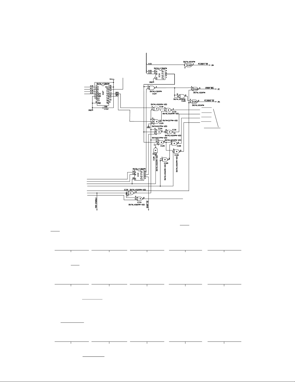
4-4. Memory chip selection circuit
The RAM chip select signals made by the following circuit.
There are 4 chip enable signal lines for RAM selection and 3 chip enable signal lines for Flash ROM
selection (including Memory cassette).
RAM1 CE
RAM2 CE
RAM3 CE
RAM4 CE
RAM1 CE is for RAM 1 chip
enable signal.
RB1
RB2
RB3
RB4/CB1
FB1
RAM enable
ARC RESET
RAM1 selection
The RAM1 is selected by the RAM enable signal "H" and the 2CS signal " L" of output pin No.13 . The
2SC signal becomes "L" when the CPU address is as follows:
A19 A18 A17 A16 A15 A14 A13 A12 A11 A10 A9 A8 A7 A6 A5 A4 A3 A2 A1 A0
LLHLXXXXXXXXXXXXXXXX
2XXXX
Also, the 3SC signal becomes "L" when the CPU address is as follows:
A19 A18 A17 A16 A15 A14 A13 A12 A11 A10 A9 A8 A7 A6 A5 A4 A3 A2 A1 A0
LLHHXXXXXXXXXXXXXXXX
3XXXX
Therefore, the RAM1 CE will active when the CPU adress is from 20000H to 3FFFFH with RAM enable
signal "H".
Flash ROM1 selection
The Flash 1 CE will active by the IC25 output pin No.3. This is inverted signal of A19.
A19 A18 A17 A16 A15 A14 A13 A12 A11 A10 A9 A8 A7 A6 A5 A4 A3 A2 A1 A0
HLLLXXXXXXXXXXXXXXXX
8XXXX
Therefore, the Flash1 CE will active when the CPU adress is from 80000H to FFFFFH.
— 11 —
Page 14
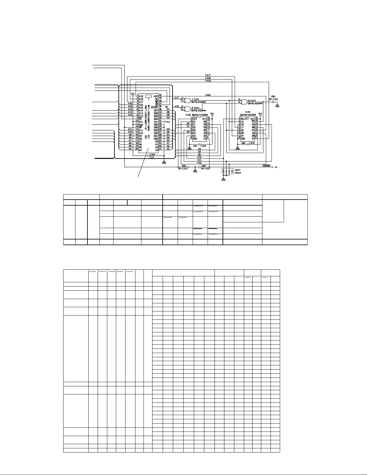
4-5. Flash ROM1 address circuit
The Flash ROM1 address signals FA17 to FA20 are made by the following circuit.
The Flash ROM1 (LH28F016SCT-L95, 16M bits) is used for the application program.
Flash ROM1 (16M bits)
CPU address BANK port Flash memory address NOTE
A19 A18 A17 FC2 FC1 FC0 BANK FA20 FA19 FA18 FA17 Memory block No. 8M bank 16M bank
H L L L L L 0 L L A18 A17 02 to 07
L H L L H 1 L H A18 A17 0A to 0F
H L H X X 2 A18 A17 L L 08,09
L H L 3 H L A18 A17 12 to 17
L H H 4 H H A18 A17 1A to 1F
H H H X X X Common LLLL00,01 Common
10,11,18,19
4-6. Memory map
The memory table is as follows:
RAM enable 2 CS 3C S 4 C S 8C S C C S A18 A 19 RAM BANK Flash BANK RAM1 Flash1
H L HHHHLLCOMXXXXXXXXLLHX
H HLHHHLLCOMXXXXXXXXLHHX
H HHLHHHL 0L HL L XXXXHXHX
H HHLHHHL L L HL X XXXHXHX
H HHLHHHL L HHL XXXXHXHX
H HHLHHHL 2LLLHLXXXHXHX
L XXXXXXX XXXXXXXXHXXX
X HHLHHHL HLLLXLHLHXHX
X HHLHHHL LLLLLLLLHXHX
X HHLHHHL XLLLXLXHHXHX
X HHHLHLH XXXXXLXHHXHX
H HHHL HLH XXXXXXXLHXLA18
H HHHHL HH XXXXXXXXHXLA18
No. RB0 RB1 RB2 RB3 RB4 FB0 FB1 FB2 CS A16 C S A18
1HHL L X XXXHXHX
HL HL X XXXHXHX
HHHLXXXXHXHX
3HL L HL XXXHXHX
4LHL HL XXXHXHX
5HHL HLXXXHXHX
6LL HHL XXXHXHX
7HL H HLXXXHXHX
8LHHHLXXXHXHX
9HHHHLXXXHXHX
10L L L HHXXXHXHX
11HL L HHXXXHXHX
12L HL HHXXXHXHX
13HHL HHXXXHXHX
14L L HHHXXXHXHX
15HL HHHXXXHXHX
16LHHHHXXXHXHX
17HHHHHXXXHXHX
HLLLXHHLHXHX
HLLLLLLLHXHX
LLLLHLLLHXHX
HLLLHLLLHXHX
LLLLLHLLHXHX
HLLLLHLLHXHX
LLLLHHLLHXHX
HLLLHHLLHXHX
XLLLXHXHHXHX
XXXXXHXHHXHX
— 12 —
Page 15
Memory map
00000h CPU internal memory
Mask ROM 128K
RAM 5K
0FFD0h External I/O Mapping 16bytes
0FFE0h
20000h
RAM1 128 K bytes
40000h
Not used
80000h
Flash 1 384 K bytes 16 M bit
(for
A0000h Application 8 M bit
program area) 4 M bit
2 M bytes Bank0 Bank1 Bank2 Bank3 Bank4
C0000h
E0000h 04,05 12,13 18,19 24,25 30,31
FFFFFh (00,01)
Bank area
Common area (o3,02) (0B,0A) (09,08) (13,12) (1B,1A)
128 K bytes
Block
06,07
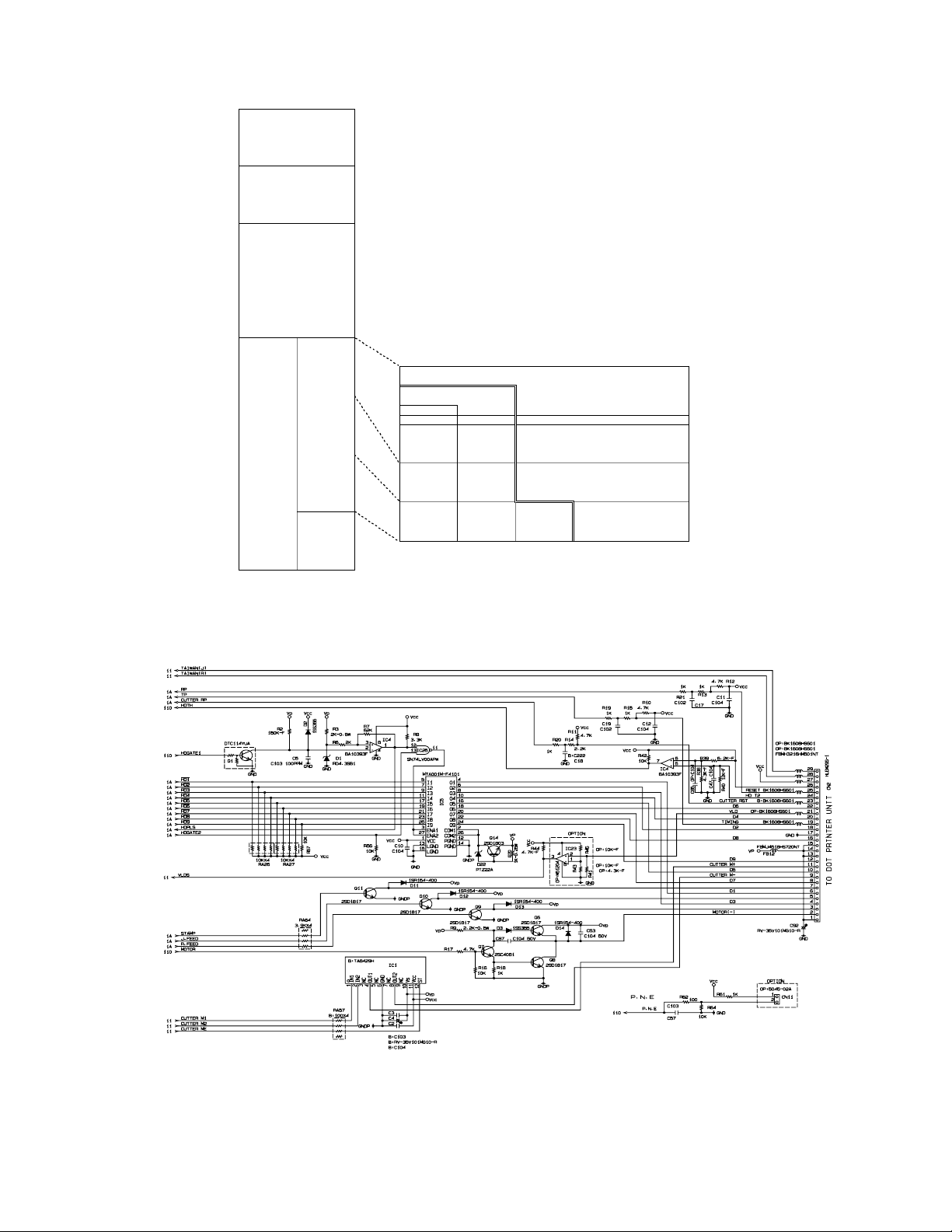
4-7. Printer drive circuit
The printer drive circuit is as follows:
00,01 08,09 14,15 20,21 26,27 Block No.
(07,06) (0F,0E) (19,18) (17,16) (1F,1E) (Memory Block)
02,03 10,11 16,17 22,23 28,29
(05,04) (0D,0C) (11,10) (15,14) (1D,1C)
IC5 (MTA001M-F4101) is the head pin driver IC. And, the Transistors Q6,Q7 and Q8 are the motor drive
circuit. The IC1 (TA8429H) is the auto paper cut driver circuit.
— 13 —
Page 16
4-8. RS232C port COM1 circuit
The COM1 circuit is as follows:
The COM1 port pin location is as shown below:
Signal
CD
RxD
TxD
DTR
GND
DSR
RTS
CTS
CI
Pin
1
2
3
1
2 3 4 5
4
5
6 7 8 9
6
7
8
9
— 14 —
Page 17

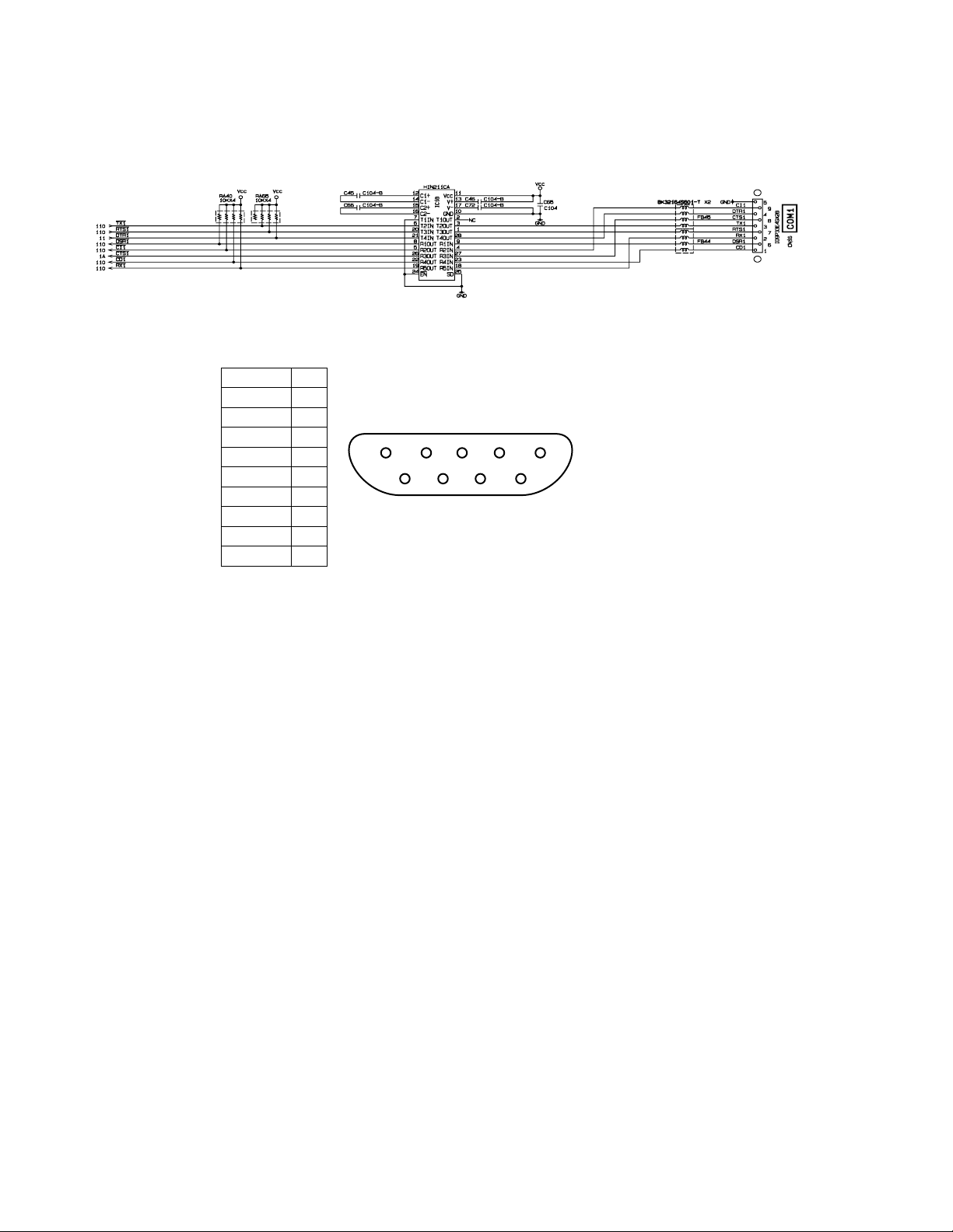
4-9. RS232C port COM2 and COM3 circuit
The circuits of COM2 and COM3 are as follows:
TP48
COM2
COM3
The COM2, and COM3 port pin locations are as shown below:
COM2 port COM3 port
Signal
NC
RxD
TxD
DTR
GND
DSR
RTS
CTS
VCC (+5V)
Pin
1
2
3
4
5
6
7
8
9
Signal
NC
RxD
TxD
DTR
GND
DSR
RTS
CTS
NC
Pin
1
2
3
1
2 3 4 5
4
5
6 7 8 9
6
7
8
9
— 15 —
Page 18
4-10. To mount optional circuit
The following optional circuits are provided for this model CE6800.
1. Multi-drawer circuit
2. Paper near end circuit
1) Multi-drawer kit (Only Drawer 2)
1-1. Prepare the following parts kit for multi-drawer circuit. The parts kits are supplied from sales division.
MDL-10 ------------- Multi-drawer kit
1-2. Check whether the parts of multi-drawer kit are as follows:
Code No. Parts Name Specification Q'ty
10006121 Drawer connector cable E440721A*1 1
62481534 Extension cable for Drawer E440714*1 1
59000209 Screw 3X4ZMC-3. 1
1-3. Connect the drawer connector cable to the main PCB by solder.
Drawer2 Drawer3 Drawer4
Red
Brown
Black
1-4. Open the back cover of lower cabe to release the 2 screws. Then, connect the necessary extension
cable for drawer. In this case, do no forget to fix the FG wire of the extension cable to the frame ground
by the screw.
Release the 2 screws and open the
back cover of lower case.
Connect the extension
drawer cable to the
drawer connector.
Fix the FG wire of the
extension drawer cable by
screw of the parts kit.
1-5. Connect 1 pin FG connector of the drawer extension cable to the drawer 1 pin connector.
Close the back cover of lower case by 2 screws.
— 16 —
Page 19
5. DIAGNOSTIC OPERATION
5-1. To start the diagnostic program
1. Plug the power cord into an AC outlet.
2. Set the mode switch to "OFF" position.
3. While pressing the "Jounal feed " button,
turn the mode switch to "PRG" position.
4. Release the "Journal feed" button.
5. Input "99990000" and press "ST" ("#2" key).
6. Diagnostic program is executed.
5-2. Check item
The following test can be checked in the diagnostic test.
1. Key code test
2. Switch status test
3. Individul function test
5-3. Operation of each test
1. Key code test
When pressing a key, the machine displays
the following key code.
HARD KEY CODE TABLE
RF JF 077 070 068 066 066 060 054 048 042 036 030 024 018
087 082 076 069 067 065 065 059 053 047 041 035 029 023 017
086 081 075 789064 058 052 046 040 034 028 022 015
085 080 074 456063 057 051 045 039 033 027 014 016
084 079 073 123062 056 050 044 038 032 026 020 021
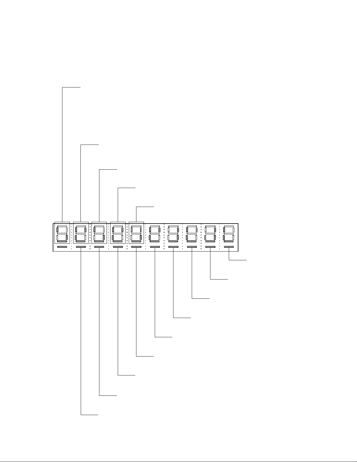
DISPLAY
XXX zz
Hard key code
089 090 091 092 093 094
095 096 097 098 099 100
Key borad information
11: Stroke Key
10: Stroke + Flat Key
01: Full Flat Key
083 078 072 0 11 12 061 055 049 043 037 031 025 019 013
Note: "014" button is work for "#2" key. "013" button is work for "#1" key.
— 17 —
Page 20
5-4. Switch status test
Press "C" button or changing the switch condition,the switch status is appeared on the transaction place of the
display. The clerk key switch condition is showen at the 6 and 7 digit number's place of display. For the clerk
button model, the pressed LED will light on.
[DISPLAY]
Mode switch status
0 : No connetion
1 : PGM
2 : RF
3 : REG1
4 : REG2
5 : X
6 : Z
7 : XZ2
8 : OFF
Menu switch conditon
0 : Switchs are both off condition.
1 : Menu 1
2 : Menu 2
INIT switch
0 : Switch off
1 : Switch on
ROM switch
0 : Switch off
1 : Switch on
Fiscal ROM Board condition
0 : Connected
1 : Not connected
Paper near end sensor
Off : Normal (Paper end switch OFF)
On : Near end (Paper and switch ON)
Drawer sensor
Off : Drawer close
On : Drawer open
2nd Display condition
Off : Connected
On : Not connected
Printer connection sensor
Off : Connected
ON : Not connected
Journal head sensor
Off : Head down
ON : Head up
Receipt head sensor
Off : Head down
ON : Head up
Journal paper sensor
Off : Paper in
ON : Paper out
Receipt paper sensor
Off : Paper in
ON : Paper out
ROM cassette condition
Off : Not mounted
On : Mounted
— 18 —
Page 21
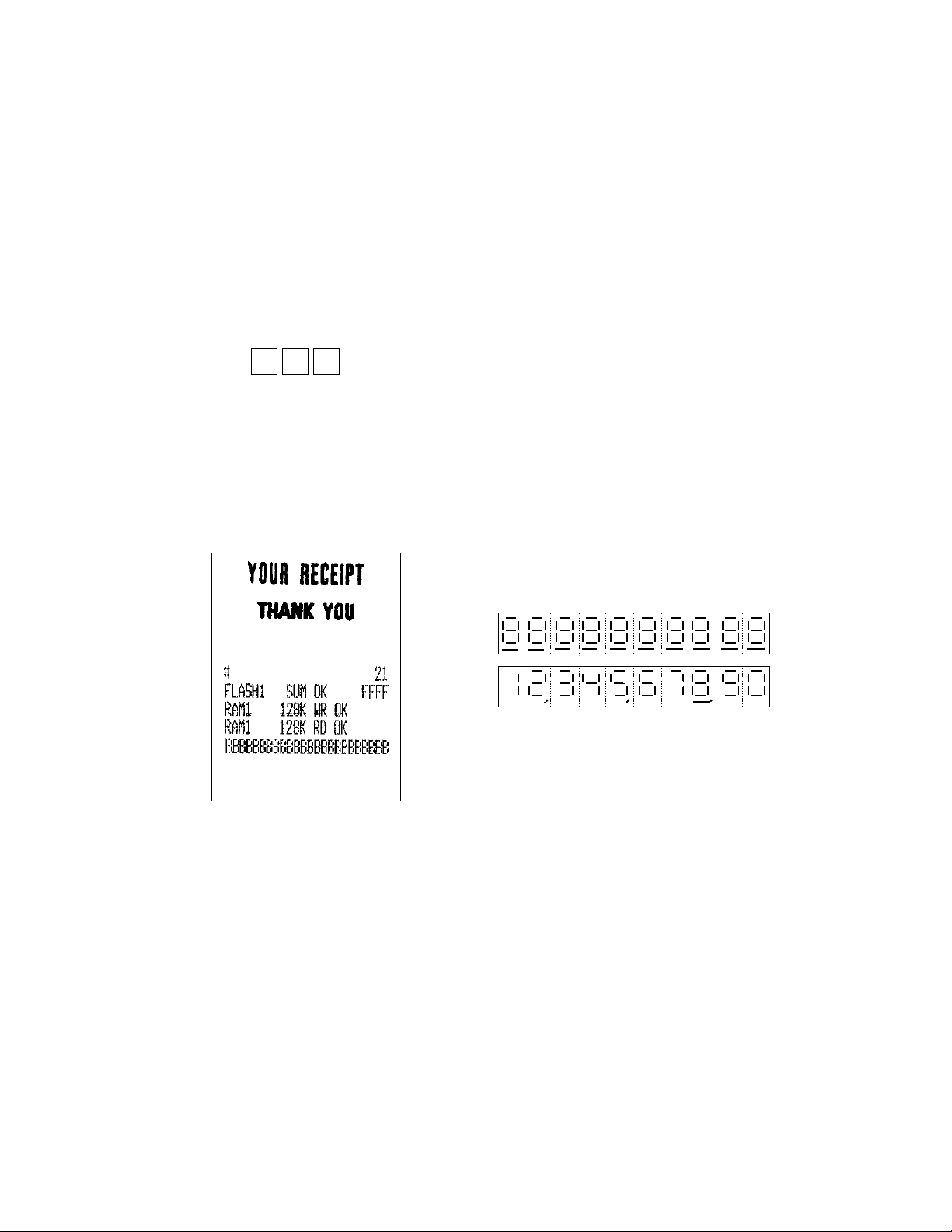
5-5. Individual function test
1) Series test
This test will perform the following tests in series.
1. Display test (All dot and segment trun on.)
2. RAM read after write test (one time)
3. Print test (one time)
4. Time display test
5. Drawer open test
6. Receipt issue test
7. Display test (1234567890 display)
Operation : X 1 #2 Key
Function X: 0= Automatic RAM capacity detection
1= RAM1 (128K) test only
NOTE : CE-6800 has the only RAM1 (128 K bytes).
[PRINT] [DISPLAY]
NOTE : In case of error, the following error message will be printed.
RAM1 128K WR ERR!! 00 000000 ----------- When the write error is happened.
Error Bank and Address
RAM1 128K RD ERR!! 00 000000 ----------- When the verified data error is happened.
FLASH SUM ERR!! 1234 ----------- Check sum of Flash1 is not "FFFF".
Caliculated check sum
— 19 —
Page 22
2) Print aging test (R/J printer)
This test will check the R/J printer continuously until pressing some key button or turn off the mode switch.
Operation : n1 Y X 2 #2 Key
Function X: 0= Print 45 times test pattern without paper cut in a minute.
1= Print 15 times test pattern with paper cut in a minute.
Y: 0= Normal print
1= Continuously print
n1: 0= Display test pattern
1= All segment will light on.
[PRINT] [DISPLAY]
Segment display (Test pattern)
3) Print test (R/J printer)
This test will check the R/J printer. To stop the continuous printing, press some key button or turn off the
mode switch.
Operation : n1 n 0 X 0 #2 Key
Function X: 0= One time print
1= Continuously print
n: 0= Display test pattern
1= All segment will light on.
n1: 0= Print test pattern
1= Print all "B"
[PRINT] [DISPLAY]
Segment display (Test pattern)
Print all "B"
Print test pattern
— 20 —
Page 23
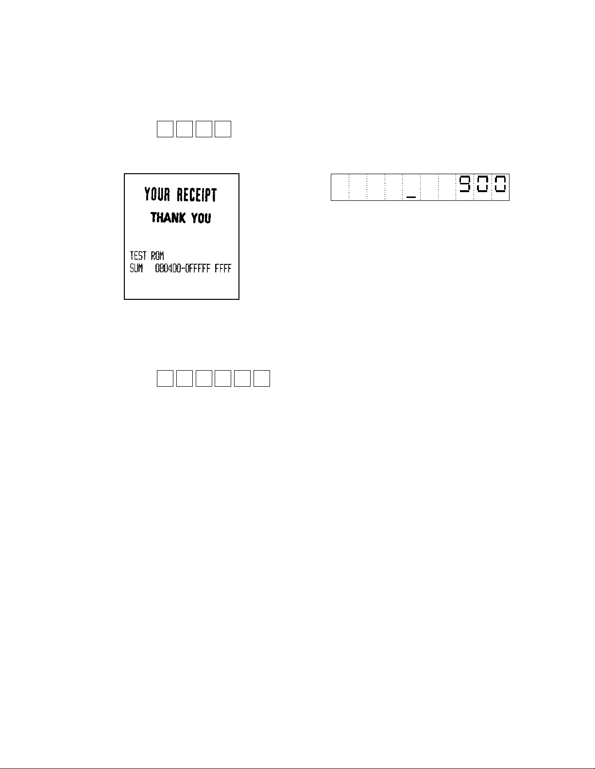
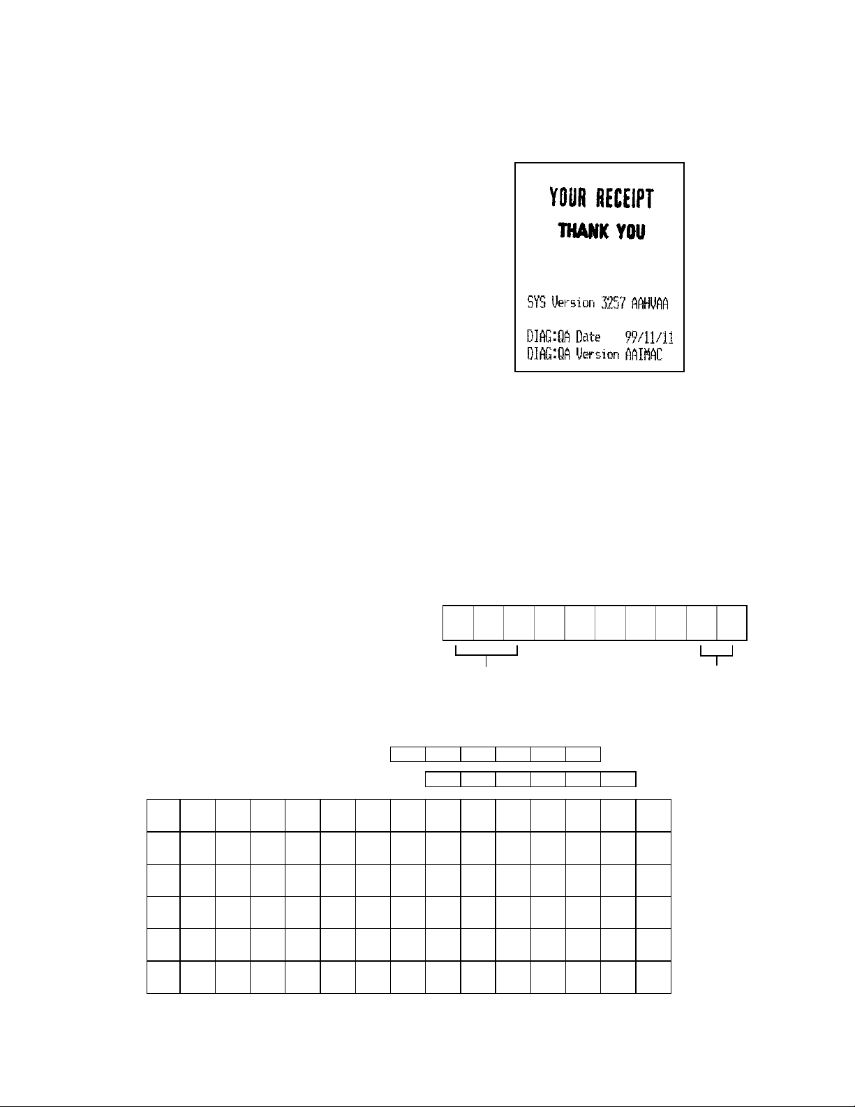
4) Flash1 ROM check
This test will check the Flash 1 ROM. This test will print the version name and check sum on the receipt
as shown in sample print. When using several bank, the each version name and check sum will be printed
after this sample data.
Operation : 9 0 0 #2 Key
[PRINT] [DISPLAY]
5) Drawer open check
This test will check the drawer open function.
Operation : d3 d2 d1 8 n 0 #2 Key
Function n: 0= Open drawer without print.
2= Open drawer with print 10lines "B" printing.
NOTE1: d3,d2,d1 are option drawer test. When input the following number, the option drawer will be
opened.
2= drawer2
3= drawer3
4= drawer4
NOTE2: Command 800 is open drawer1.
— 21 —
Page 24

6) RAM read only check
This test will check the read only check for RAM.
Perform the RAM check (EX: command "1 and #2 " ), before start of this operation.
Operation : X 5 #2 Key
Function X: 0= One time check.
1= Continuous check. To stop the test, set the mode switch to OFF.
NOTE: During the RAM test, the Receipt switch LED is blinking.
[PRINT] [DISPLAY]
7) RAM read write check
This test will check the read write check for RAM.
Operation : n 4 X 0 #2 Key
Function X: 0= Automatic RAM capacity detection
1= RAM1 (128K) test only
n: 1= Continuous check
2= In the continuous check, the print will skip when the test is no error.
4= Read only check. No writing data.
[PRINT] [DISPLAY]
— 22 —
Page 25

8) RS232 port check
This test will check the RS232 port. Connect the loop back connector before operate this check.
Operation : X 2 m 7 #2 Key
Function m: 0= One time loop check
1= Loop check continuously
2= One time loop check (Ignore the CD,CI signals. Only COM1 port)
3= Loop check continuously (Ignore the CD,CI signals. Only COM1 port)
X: 0= COM1
Test details
1) Check of the control shignals (CTS,DSR,RTS,DTR,CD,CI) Low/High level.
2) Sending data (0A5h) from Txd line and receiving data from Rxd line.
[PRINT] [DISPLAY]
LOOP BACK CONNECTOR (D-SUB9pin Female)
COM1
3pin
TxD
RxD
CTS
RTS
DTR
DSR
CD
2pin
8pin
7pin
4pin
6pin
1pin
9pin
CI
NOTE: Error code is as follows:
01= Framing error 02= Over run error 04= Parity error
40= Data error (Not 55) 80= Time out error
— 23 —
Page 26

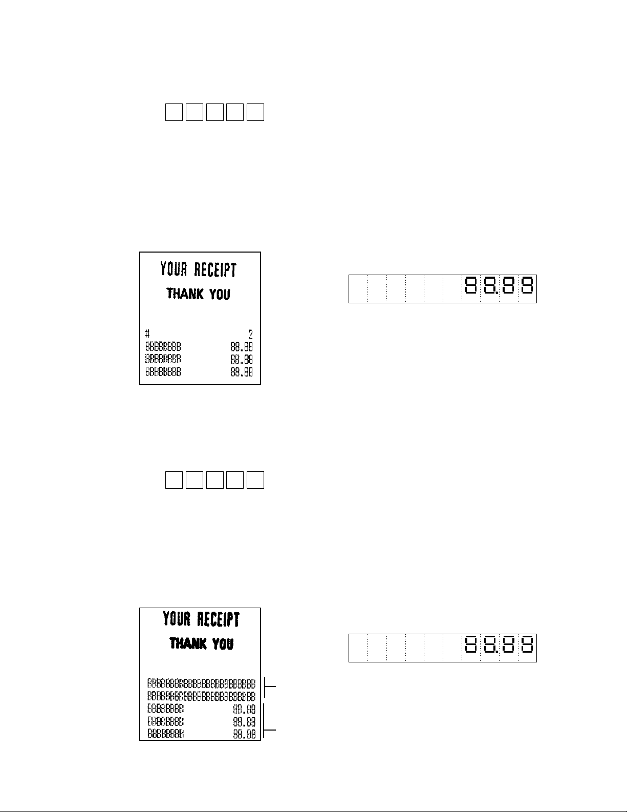
9) Print check
This test will check the print test.
Operation : s 0 0 r 8 #2 Key
Function r: 0= One time check
1= Continuously check (NOTE1)
s: 0= Receipt/Journal print mutually
1= Receipt print only
2= Journal print only
NOTE1: To stop this test, press any key or set the mode switch to OFF position.
[PRINT] [DISPLAY]
10) All charactor print check
This test will print the all charactors of the controller.
Operation : h h i i 0 s 0 1 r 8 #2 Key
Function r: 0= Print without code (24 charactors/line)
2= Print with code (16 charactors/line)
4= Print and display without code (24 charactors/line)
6= Print and display with code (16charactors/line)
s: 0= Receipt/Journal print mutually
1= Receipt print only
2= Journal print only
hh: Font selection (High code) ii: Font selection (Low code)
00= USA standard 00= USA
02= Multilingual 01= France
03= Portuguese 02= Germany
04= Canadian-French 03= England
05= Nordic 04= Denmark I
19= Euro+Multilingual 05= Sweden
51= Czecho/Poland 06= Italia
52= Hebrew 07= Spain
53= Greece 09= Norway
54= Russia 10= Denmark II
55= Latvia/Lithuania 51= Czecho/Poland
56= Arabia 52= Hebrew
99= User option 53= Greece
54= Russia
55= Latvia/Lithuania
56= Arabia
99= User option
— 24 —
Page 27

NOTE: When use the command ptrint and display, press #1 key (Cash AMT tender key) to display and
print the next line. To stop this test, press any key or set the mode switch to OFF position.
[PRINT] [DISPLAY]
11) Time and date display test
The machine will display the time .
By #2 Key, the display will change the date and time.
Opeartion : 9 #2 Key
[PRINT] [DISPLAY]
Press #2 key to change the display.
— 25 —
Page 28

12) Date time set test
The machine will set the time or the date.
Opeartion : n1 n2 n3 n4 n5 n6 X 9 #2 Key
Function X: 0= Time set (n1 n2: Time, n3 n4: Minute, n5 n6: Second)
1= Date set (n1 n2: Year, N3 n4: Month, n5 n6: Day)
[PRINT] [DISPLAY]
13) COM1 online test
This operation will test the COM1 online function. This test need the reception machine as shown below;
Send
ECR
Cable length = Max. 15m
COM1 COM1
Receive
ECR
Cross cable
Wiring diagram for the connection cable Loop back connector
Signal Pin
CD 1
RxD 2
TxD 3
DTR 4
GND 5
DSR 6
RTS 7
CTS 8
CI 9
Signal Pin
CD 1
RxD 2
TxD 3
DTR 4
GND 5
DSR 6
RTS 7
CTS 8
CI 9
Txd
Rxd
CTS
RTS
DTR
DSR
CD
CI
COM1
3pin
2pin
8pin
7pin
4pin
6pin
1pin
9pin
COM1 COM1
Opeartion : z z b m 7 2 X 7 #2 Key
Function b: Baud rate selection
0= 19,200 bps 1= 9,600 bps 2= 4,800bps 3= 2,400bps 4= 38,400 bps
m: Test Mode selection
0= Self loop test 1= Reception mode 2= Send mode
zz: Time out number (seconds) input between data
(default is 3 seconds. Input zz, zz seconds will be the time of time out.)
X: 0= Normally select 0.
1= When error is happened, print error receipt before retry operation.
— 26 —
Page 29

Test procedure
1) Operate the send machine first. The send machine will wait the "C" signal (send request) reception
from the reception machine.
The send machine will wait the send request signal about 30 seconds. When it is over 30 seconds,
the time out error will be printed on the receipt.
2) Operate the reception machine. Then, the both machines are communicated each others. This time
first block data wait time is 5 seconds. The total resend request time is 5 time.
3) During communication waiting time, the display will show the "-" brinking on the most left side digit of
segment display. When the data is OK, the reception/transmission packet number will be displayed
on the segment display.
NOTE1: To stop this opeartion, press any or trun off the mode key switch.
NOTE2: The send packet data format is as follows:
( Communication format is 8 bits, even parity, stop bit= 1bit fixed.)
STX
03h
Block counter
2 bytes
Data (55h X 1,020 pcs.)
Total 1,024 bytes
[PRINT] [DISPLAY]
Normal End
Error End (Time out error)
E : Error status
(01 : Framing error)
(02 : Over run error)
(04 : Parity error)
(40: Transmit/ Receive data error/ Data is not 55.)
(80 : Time out error)
LRC
Count data block
5-6. To exit the diagnostic mode
To escape the diagnostic mode, execute INITIALIZE (MAC) operation.
— 27 —
Page 30

6. IC DATA
1. BA10393F-E2 2. BA12003BF-E2
BA10393/BA10393F
OUT1
–IN1
+IN1
V
EE
3. HA17431PA
1
2
3
4
REF
2.500 V
1ch
–+
2ch
+–
+
–
8
7
6
5
V
CC
OUT2
–IN2
+IN2
K
123
IN1
IN2
IN3
IN4
IN5
IN6
IN7
GND
1
2
3
4
5
6
7
8
16
OUT1
15
OUT2
14
OUT3
13
OUT4
12
OUT5
11
OUT6
10
OUT7
9
COM
4. HD74LVC374ATELL
A
REF A
K
TO-92MOD
— 28 —
Page 31

5. HIN211CA-T
6. HY628100ALLG-70
7. LC7932M-TE-R
— 29 —
Page 32

8. LH28F016SCT-L95A
Name and FunctionTypeSym
A0-A
20
DQ0-DQ
7
INPUT
INPUT/
OUTPUT
CE# INPUT
RP# INPUT
WE# INPUT
RY/BY# OUTPUT
V
PP
V
cc
SUPPLY
SUPPLY
ADDRESS INPUTS: Inputs for addresses during read and write operations.
Addresses are internally latched during a write cycle.
DATA INPUT/OUTPUTS: Inputs data and commands during CUI write cycles;
outputs data during memory array. status register, and identifier code read
cycles. Data pins float to high-impedance when the chip is deselected or
outputs are disabled. Data is internally latched during a write cycle.
CHIP ENABLE: Activates the device's control logic, input buffers, decoders,
and sense amplifiers. CE#-high deselects the device and reduces power
consumption to standby levels.
RESET/DEEP POWER-DOWN: Puts the device in deep power-down mode
and resets internal automation. RP#-high enabies normal operation. When
driven low. RP# inhibits write operations which provides data protection during
power transitions. Exit from deep power-down sets the device to read array
mode. RP# at VHH enables setting of the master lock-bit and enables
configuration of block lock-bits when the master lock-bit is set. RP# = VHH
overrides block lock-bits theredy enabling block erase and byte write
operations to locked memory blocks. Block erase, byte write. or lock-bit
configuration with VHH<RP#<VHH produce spurious results and should not be
attempted.
OUTPUT ENABLE: Gates the device's output during a read cycle.OE# INPUT
WRITE ENABLE: Controls writes to the CUI and array blocks. Addresses and
data are latched on the rising edge of the WE# pulse.
READY/BUSY#: Indicates the status of the internal WSM. When low, the
WSM is performing an internal operation (block erase, byte write, or lock-bit
configuration). RY/BY#-high indicates that the WSM is ready for new
commands, block erase is suspended, and byte write is inactive, byte write is
suspended, or the device is in deep power-down mode. RY/BY# is always
active and does not float when the chip is deselected or data outputs are
disabled.
BLOCK ERASE, BYTE WRITE, LOCK-BIT CONFIGURATION POWER
SUPPLY:For erasing array blocks, writing bytes, or configuring lock-bits. With
VPP ≤ V
, memory contents cannot be altered, Block erase, byte write, and
PPLK
lock-bit configuration with an invalid VPP (see DC Characteristics) produce
spurious results and should not be attempted.
DEVICE POWER SUPPLY:Internal detection configures the device for 2.7 V,
3.3 V or 5 V operation. To switch from one voltage to another, ramp V
CC
down
to GND and then ramp VCC to the new voltage. Do not float any power pins.
With VCC ≤ V
operations at invalid V
, all write attempts to the flash memory are inhibited. Device
LKO
voltage (see DC Characteristics) produce spurious
CC
results and should not be attempted. Block erase, byte write and lock-bit
configuration operations with VCC < 3.0 V are not supported.
GROUND: Do not float any ground pins.GND SUPPLY
NO CONNECT: Lead is not internal connected: it may be driven or floated.NC
— 30 —
Page 33

9. LM2576HVT-5.0LB03
10.MTA001M-F4101
— 31 —
Page 34

11.S-80823ANNP-EDL/S-80835ALNP-EAZ
(1) Nch open drain active low output
12.SN74AHC1G00DCKR
(2) CMOS active low output
S-808XX AX XX - XXX - T2
Tape spec. IC direction
Production short No.
Package No.
NP: SC-82AB
MP: SOT-23-5
UP: SOT-89-3
Y: TO-92
Output
N: Nch open drain (Active "L")
L: CMOS (Active "L")
Detection Voltage X 10 times
13.SN74HC157APWR
— 32 —
Page 35

14.SN74HC27PWR
15.SN74LV00APWR
16.SN74LV02APWR
17.SN74LV08APWR
— 33 —
Page 36

18.SN74LV138APWR
19.SN74LV139APWR
— 34 —
Page 37

20.SN74LV165APWR
— 35 —
Page 38

21.SN74LV165APWR
22.SN74LV174APWR
— 36 —
Page 39

23.SN74LV32APWR
24.SN74LV74APWR
— 37 —
Page 40

7. PCB LAYOUT
MAIN PCB (Front side)
— 38 —
Page 41

MAIN PCB (Back side)
— 39 —
Page 42

8. CIRCUIT DIAGRAM
MODEL : CE-6800 (EX-475EP)
CONTENTS
1. LOCATION OF PRINTED CIRCUIT BOARD .......................................................................... 40
2. MAIN PCB CIRCUIT ................................................................................................................ 41
2-1. MAIN PCB CIRCUIT (1/6) ............................................................................................... 41
2-2. MAIN PCB CIRCUIT (2/6) ............................................................................................... 42
2-3. MAIN PCB CIRCUIT (3/6) ............................................................................................... 43
2-4. MAIN PCB CIRCUIT (4/6) ............................................................................................... 44
2-5. MAIN PCB CIRCUIT (5/6) ............................................................................................... 45
2-6. MAIN PCB CIRCUIT (6/6) ............................................................................................... 46
3. LED DISPLAY (MAIN DISPLAY) ............................................................................................. 47
3-1. MAIN PCB CIRCUIT (1/3) ............................................................................................... 47
3-2. MAIN PCB CIRCUIT (2/3) ............................................................................................... 48
3-3. MAIN PCB CIRCUIT (3/3) ............................................................................................... 49
4. KEYBOARD ............................................................................................................................. 50
5. CLREK SW .............................................................................................................................. 51
6. POP-UP DISPLAY ................................................................................................................... 51
7. POWER SUPPLY CIRCUIT .................................................................................................... 52
8. MODE SWITCH ....................................................................................................................... 53
— 40 —
Page 43

— 41 —
CASIO COMPUTER CO.,LTD.
CE-6800
(EX-475P)
Model Name
SYSTEM BLOCK DIAGRAM
Drawing No.
E140329P
Page 44

— 42 —
— 42 —
Page 45

— 43 —
RAM3 and RAM4 are option.
For CE6800, the Flash ROM2
is not used.
Page 46

— 44 —
Page 47

— 45 —
Page 48

— 46 —
Page 49

— 47 —
DRW3 and DRW4 are not used.
Page 50

— 48 —
Page 51

— 49 —
Page 52

— 50 —
Page 53

— 51 —
Page 54

— 52 —
Page 55

— 53 —
Voltage selector is not used for CE-6800.
Page 56

— 54 —
Page 57

— 55 —
Page 58

9. PARTS LIST
PARTS LIST
MODEL : CE-6800 (EX-475EP)
CONTENTS
EXPLODE VIEW............................................................................................................................ 57
1. MAIN PCB BLOCK .................................................................................................................. 59
2. MAIN DISPLAY BLOCK ..........................................................................................................60
3. CUSTOMER DISPLAY BLOCK ............................................................................................... 61
4. BUTTON BLOCK ..................................................................................................................... 61
5. POWER SUPPLY BLOCK ....................................................................................................... 62
6. CONNECTOR BOARD ............................................................................................................ 62
7. CLERK SWITCH CIRCUIT ...................................................................................................... 63
8. UPPER CASE BLOCK ............................................................................................................63
9. LOWER CASE BLOCK............................................................................................................63
10. PRINTER BLOCK .................................................................................................................... 63
11. OTHERS .................................................................................................................................. 64
12. PRINTER (M-U420B-031) ....................................................................................................... 65
13. DRAWER ................................................................................................................................. 70
DL-2771 ................................................................................................................................... 70
NOTES :
1. Price and specifications are subject to change withput prior notice.
2. As for spare parts order and supply, refer to the “GUIDEBOOK for Spare Parts Supply”, published
separately.
3. The numbers in item column corespond to the same numbers in drawing.
4. CASIO does not supply the spare parts without parts code.
5. Remarks
Q'ty : Quantity used per unit
RANK: A = Essential
B = Stock recommended
C = Less recommended
X = No stock recommended
— 56 —
Page 59

11
LED -
Numeric LED
5
4
PCB Blank
3
7
55
CASIO CE-6800
6
10
56
82
31
56
50
8
9
52
85
86
49
2
D
A
F
48
51
46
26
39
38
33
27
47
F
22
21
7
19
23
9
8
6
5
3
4
2
.
1
00
0
24
25
20
17
16
A
18
15
13
12
14
34
29
30
28
35
36
37
32
— 57 —
Page 60

70
54
53
67
42
D
87
77
76
73
84
78
70
61
70
75
79
74
43
41
40
63
64
44
C
81
E
80
45
62
66
C
1
72
E
65
68
59
60
B
Battery only
58
B
83
57
66
69
86
71
71
For Drawer fix
— 58 —
Page 61

N
Item Code No. Parts name Specification Q Price code R
1 10049420 PCB ASSY/E475-1 E240672*9 1 EF A
F1 30007777 FUSE 230.600 1 AE A
IC10 10042378 LSI UPD784215GC201-8EU 1 BW A
IC1 21145832 IC/MOS TA8429H 1 AZ A
IC12,20 10029099 IC/MOS SN74HC74APWR 2 AD A
IC40 21120819 IC HIN202CBN-T 1 AP A
IC39 21120820 IC HIN211CA-T 1 AT A
IC18 10034262 IC HIN211EIA 1 BC A
IC2 10005690 IC/RESET S-80823ANNP-EDL-T2 1 AB A
IC24 10004413 IC/MOS SN74LV32APWR 1 AB A
IC25,28 10003984 IC/MOS SN74LV00APWR 2 AB A
IC26,27 10005671 IC/MOS SN74LV138APWR 2 AD A
IC29 10005664 IC/MOS SN74HC27PWR 1 AC A
IC3,19 20061691 LSI HY628100ALLG-70 2 BP A
IC6 10010984 LSI LH28F016SCT-L95A 1 CJ A
IC30,41 10005642 IC/MOS SN74LV02APWR 2 AB A
IC31,38 10005669 IC/MOS SN74LV139APWR 2 AD A
IC33 10005659 IC/MOS SN74LV08APWR 1 AB A
IC4 21120821 IC/COMPARATOR BA10393F-E2 1 AB A
IC22,42 10005666 IC/MOS SN74LV174PWR 2 AD A
IC14 10005721 IC/MOS SN74LV244APWR 1 AF A
IC16,43 10005691 IC/MOS SN74HC157APWR 2 AE A
IC44 10005651 IC/MOS SN74AHC1G00DCKR 1 AB A
IC45 10005655 IC/RESET S-80835ALNP-EAZ-T2 1 AB A
IC5 21120831 IC/MOS MTA001M-F4101 1 BH A
IC7 10005678 IC/MOS HD74LVC374ATELL 1 AF A
X1 24088404 OSCILLATOR/CERAMIC CSTCV12. 5MTJ0C4-T 1 AD A
X2 25203445 OSCILLATOR/CRYSTAL C-002RX(M90-76) 1 AD A
D1 23153126 DIODE/ZENER RD4.3SB1-T1 1 AA B
D2,3,5,10 23901820 DIODE 1SS355TE-17 4 AA B
D22 23153127 DIODE/ZENER PTZTE-2522A 1 AB B
D4 23153125 DIODE/ZENER RD22UJN1-T1 1 AA B
D6,9,11-16,23 23902058 DIODE 1SR154-400TE25 9 AB B
FB12 30008098 INDUCTOR FBMJ4516HS720NT 1 AB B
FB30-33,37,44,45 30132359 INDUCTOR BK3216-4S601-T 7 AA B
FB5,6,8,9,24 30450028 INDUCTOR BK1608HS601-T 5 AA B
FB7,28,29,41 30008056 INDUCTOR FBMH3216HM501NT 4 AB B
Q1,13 79113038 TRANSISTOR/DIGITAL DTC114YUAT106 2 AA B
Q12 22501601 TRANSISTOR 2SC4617TLQ 1 AA B
Q14 22501618 TRANSISTOR 2SD1803S/T-TL 1 AD B
Q2,5 22501602 TRANSISTOR 2SD1834T100 2 AB B
Q6,8-11 22501619 TRANSISTOR 2SD1817-TL 5 AE B
Q7 22501605 TRANSISTOR 2SC4081T106 1 AA B
IC9,13 36106859 SOCKET/IC DILB32P-8JK 2 AD C
BZ1 32402089 BUZZER PKM22EPT-2001 1 AE C
C14,15,33 28073626 CAPACITOR/ELECTROLYTIC RV3-10V221MF80-R 3 AB C
C27 28077127 CAPACITOR/ELECTROLYTIC RV2-50V010M-R 1 AA C
C29 28073647 CAPACITOR/ELECTROLYTIC RV2-16V101MS-R 1 AA C
C4,40,92 28077818 CAPACITOR/ELECTROLYTIC RV-35V101MG10-R 3 AB C
CA1-5 28073645 CAPACITOR/MODULE MNA145A470KK 5 AA C
CA6,7 10004467 CAPACITOR/MODULE CAF13CH330K50AT 2 AA C
CN1,18 35005846 CONNECTOR 53253-0210 2 AA C
CN13 35017728 CONNECTOR B14B-PHDSS 1 AB C
CN16 30007917 PLUG/D-SUB CONNECTOR ID9P33E4GX28 1 AK C
CN12 35405180 CONNECTOR HFW20S-2STE1 1 AC C
CN10 10005684 CONNECTOR IMSA-9830S-40Y930 1 AI C
CN8 10005643 CONNECTOR HFW28S-2STE1 1 AD C
CN2 35405200 CONNECTOR HLEM29S-1 1 AC C
CN3 35021809 CONNECTOR B3B-PH-SM3-TB 1 AC C
1. Main PCB block
N
N
N
N
N
N
N
N 10020873 SPACER/PCB E441062-1 1 AC C
N
N
N
- 59 -
Page 62

N
Item Code No. Parts name Specification Q Price code R
CN9 35802371 CONNECTOR B4P-VH 1 AB C
R54 26523053 RESISTOR/METAL FILM ERX1ANJ5R6H 1 AA C
N
RA49-57 27975518 RESISTOR/CHIP NETWORK RAC1608-1014DJT 9 AA C
RA24,28,31,32,63 10005641 RESISTOR/CHIP NETWORK RAC1608-4704DJT 5 AA C
27,35,40,47,48,61,65
RA60 26601159 RESISTOR/CHIP NETWORK RAC1608-4724DJT 1 AA C
RA64 10005679 RESISTOR/CHIP NETWORK RAC1608-3924DJT 1 AA C
SW1 30008096 SWITCH SKQLLD-T 1 AD C
C54 CAPACITOR/CHIP TMK107B102KZ-T 1 X
C30,56,91 CAPACITOR/CHIP UMK107CH101JZ-T 3 X
C36 CAPACITOR/CHIP UMK107CH100DZ-T 1 X
C38 CAPACITOR/CHIP UMK107CH180JZ-T 1 X
72,77,78
C5 CAPACITOR/CHIP ECHU1C103GB5 1 X
C53,87 CAPACITOR/CHIP UMK212F104ZR-T 2 X
C3,57 CAPACITOR/CHIP TMK107B103KZ-T 2 X
C17-19 CAPACITOR/CHIP TMK107B222KZ-T 3 X
R10,11,12,17 RESISTOR/CHIP RC1608-472-J-T 4 X
1
R14 RESISTOR/CHIP RC1608-222-J-T 1 X
R2 RESISTOR/CHIP RC1608-154-F-T 1 X
R23 RESISTOR/CHIP RC1608-563-F-T 1 X
R24,44 RESISTOR/CHIP RC1608-472-F-T 2 X
R26 RESISTOR/CHIP RC1608-104-J-T 1 X
R27 RESISTOR/CHIP MCR03EZHF3600 1 X
R28 RESISTOR/CHIP MCR03EZHF1540 1 X
R3 RESISTOR/CHIP MCR50JZHJ202 1 X
R32 RESISTOR/CHIP RC1608-334-J-T 1 X
R33 RESISTOR/CHIP RC1608-105-J-T 1 X
R38 RESISTOR/CHIP RC1608-432-F-T 1 X
R39 RESISTOR/CHIP RC1608-622-F-T 1 X
64,72,74,83, *3,*6
R40 RESISTOR/CHIP RC1608-123-F-T 1 X
R5,62 RESISTOR/CHIP RC1608-101-J-T 2 X
R59 RESISTOR/CHIP RC1608-822-J-T 1 X
R6 RESISTOR/CHIP RC1608-202-J-T 1 X
R60,68 RESISTOR/CHIP RC1608-563-J-T 2 X
R7 RESISTOR/CHIP RC1608-623-J-T 1 X
R70 RESISTOR/CHIP MCR18EZHJ102 1 X
R71,75,76,77,78 RESISTOR/CHIP RC1608-331-J-T 5 X
R8 RESISTOR/CHIP RC1608-332-J-T 1 X
R9 RESISTOR/CHIP MCR50JZHJ222 1 X
2. Main display PCB block
2 10021075 PCB ASSY/E445A-E2 E341012*1 1 DE B
IC1-3 21120823 IC/MOS BA12003BF-E2 3 AF A
IC4 10003984 IC/MOS SN74LV00APWR 1 AB A
IC5,6,10 10003982 IC/MOS SN74LV165APWR 3 AE A
IC7-9 20061703 LSI LC7932M-TE-R 3 AP A
LED1-10 24088398 LED GL8EG42 10 AA B
LED11-15 23201365 LED HDSP-5621#S02 5 AP B
Q1-5 22501603 TRANSISTOR 2SB1182TLQR 5 AC B
CA1-6 28073624 CAPACITOR/MODULE MNA145A101KK 6 AA C
CN1 35405185 CONNECTOR HFW12S-2STE1 1 AB C
N
RA1-10,21,22,25-
26601156 RESISTOR/CHIP NETWORK RAC1608-1034DJT 21 AA C
C45,46,61-63,66,69-
C1,2,6,8-13,2024,28,31,32,39,41,4752,55,59,60,65,68,74,76,
N
R13,15,18,19,20,21,25,6
R4,16,29,42,56,57,58,63,
CAPACITOR/CHIP UMK212BJ104KG-T 12 X
CAPACITOR/CHIP TMK107F104ZZ-T 35 X
RESISTOR/CHIP RC1608-102-J-T 8 X
RESISTOR/CHIP RC1608-103-J-T 14 X
SCREW 3X5 ZMC-3 1 X
- 60 -
Page 63

N
Item Code No. Parts name Specification Q Price code R
CN2 35405184 CONNECTOR HFW10S-2STE1 1 AB C
CN3 35017728 CONNECTOR B14B-PHDSS 1 AB C
CN4 35405190 CONNECTOR SFW27R-5STE1 1 AE C
CN5 35405196 CONNECTOR HFW9R-1STE1 1 AB C
CN6 35405186 CONNECTOR HFW24R-1STE1 1 AD C
FB1-30 30450028 INDUCTOR BK1608HS601-T 30 AA C
RA1-9 26523056 RESISTOR/CHIP NETWORK MNR34J5ABJ121 9 AA C
RA10,25-27 26601174 RESISTOR/CHIP NETWORK RAC1608-3314DJT 4 AA C
RA11,19,22,23,28,29 26601156 RESISTOR/CHIP NETWORK RAC1608-1034DJT 6 AA C
RA12-17,24 27975519 RESISTOR/CHIP NETWORK RAC1608-1024DJT 7 AA C
RA18,20,21 27975518 RESISTOR/CHIP NETWORK RAC1608-1014DJT 3 AA C
C1-7 CAPACITOR/CHIP TMK107F104ZZ-T 7 X
C8-10 CAPACITOR/CHIP UMK107CH101JZ-T 3 X
R1,3,5,7,9 RESISTOR/CHIP RC1608-471-J-T 5 X
R11,12 RESISTOR/CHIP RC1608-121-J-T 2 X
R13 RESISTOR/CHIP RC1608-563-J-T 1 X
R14,15 RESISTOR/CHIP RC1608-331-J-T 2 X
R2,4,6,8,10,16,17 RESISTOR/CHIP RC1608-103-J-T 7 X
10021063 HOLDER/LED E341020-1 1 AD C
3 43081401 PCB/E445A-E2-2 E340800-1 1 AF X
4 23201365 LED HDSP-5621#S02 4 AP B
5 24088398 LED GL8EG42 2 AA B
6 35405193 CONNECTOR HLW10R-2C7 1 AB C
7 35405194 CONNECTOR HLW12R-2C7 1 AB C
8 62481475 CABLE/FFC JOINT DE445 E440657-4 1 AU C
9 62481476 CABLE/FFC JOINT EE445 E440657-5 1 AU C
10 62481785 CASE/REAR DISPLAY E240511A-1 1 AH C
11 10049340 PLATE/REAR DISPLAY E240512A-8 1 AL B
12 62213988 CAP/L E210964-1 14 AB B
13 62214346 CAP/LLL E211131-1 1 AC B
14 62214025 CAP/S E311103-1 25 AA B
15 62481750 FPC E240507A-1 1 BF B
16 62467768 KEYTOP/L E210963A-4 14 AD B
17 62471471 KEYTOP/LLL E211132B-3 1 AB B
18 62467810 KEYTOP/S E311101A-4 37 AA B
19 62480990 RUBBER/CONTACT E411877A-1 52 AA B
20 62481294 SHEET/COMMON E340737-1 1 AV B
21 62473830 SPRING/COIL E411104A-1 15 AA B
22 62473837 SPRING/COIL E411104A-2 7 AA B
23 62457340 BUTTON/. E311792-10 1 AB C
24 62457330 BUTTON/0 E311792-9 1 AB C
25 62457350 BUTTON/00 E311792-11 1 AB C
26 62457250 BUTTON/1 E311792-1 1 AB C
27 62457260 BUTTON/2 E311792-2 1 AB C
28 62457270 BUTTON/3 E311792-3 1 AB C
29 62457280 BUTTON/4 E311792-4 1 AB C
30 62457360 BUTTON/5 E311116-4 1 AB C
31 62457290 BUTTON/6 E311792-5 1 AB C
32 62457300 BUTTON/7 E311792-6 1 AB C
33 62457310 BUTTON/8 E311792-7 1 AB C
34 62457320 BUTTON/9 E311792-8 1 AB C
35 62471478 FILLER/BUTTON E311197-2 7 AB C
36 62481295 SPACER E340738-1 1 AF C
37 10049447 PLATE/MODE KEY E475P E341021-27 1 AH C
38 62481296 CHASSIS/KEYBOARD E340739-1 1 AK X
62481255 FRAME/KEYBOARD E140249-1 1 AU X
3. Customer display block
62481566 HOLDER/LED E440663-1 1 AA C
N
N
N
N 62481698 PLATE/INSULATION E440781-1 1 AB C
4. Button block
N 10049428 BUTTON ASSY E140426*1 1 CV X
N
- 61 -
Page 64

N
Item Code No. Parts name Specification Q Price code R
62481434 PLATE/S E240526-4 1 X
40 10017368 PCB/E445-S1 E340808A-2 1 AM X
F1 10017330 FUSE 2371.25 1 AB A
F2 10017328 FUSE 213002 1 AD A
IC1 21120829 IC LM2576HVT-5.0LB03 1 BO A
IC2 21120809 IC HA17431PA 1 AC A
T1 10017414 TRANSFORMER TE-475-E3UA-1 1 CL A
D1 23153116 BRIDGE/DIODE D3SBA20 1 AH B
D2 23153117 DIODE D3S6M 1 AA B
D3 23153128 DIODE 1SR35-400AT-82 1 AA B
D4 23902828 DIODE RB441Q-40T-77 1 AA B
Q1 22303619 TRANSISTOR 2SD1193 1 AU B
ZD1 23153119 DIODE/ZENER RD39EB2 1 AA B
C1,2 10021055 CAPACITOR R46K124705001M 2 AC C
C5 28203730 CAPACITOR ECQ-B1H-103-JZW 1 AA C
C6 10021059 CAPACITOR/ELECTROLYTIC LPH-50V103MS4 1 BT C
C7 28190743 CAPACITOR HE40TJYB101K 1 AA C
C8 10021060 CAPACITOR/ELECTROLYTIC RJH-50V101MH4 1 AE C
C9 10021061 CAPACITOR/ELECTROLYTIC RJH-16V331MG4 1 AE C
62481438 PLATE/S E240526-6 1 X
62481439 PLATE/S E240526-7 1 X
62482157 PLATE/S E240526A-69 1 X
10049310 PLATE/S E341153-1 1 X
10049311 PLATE/S E341153-2 1 X
10049312 PLATE/S E341153-3 1 X
10049313 PLATE/S E341153-4 1 X
10049314 PLATE/S E341153-5 1 X
10049315 PLATE/S E341153-6 1 X
10049317 PLATE/S E341153-7 1 X
10049318 PLATE/S E341153-8 1 X
10049319 PLATE/S E341153-9 1 X
10049320 PLATE/S E341153-10 1 X
10049321 PLATE/S E341153-11 1 X
10049322 PLATE/S E341153-12 1 X
10049323 PLATE/S E341153-13 1 X
10049324 PLATE/S E341153-14 1 X
10049325 PLATE/S E341153-15 1 X
10049326 PLATE/S E341153-16 1 X
62481425 PLATE/S E240526-31 1 X
62481426 PLATE/S E240526-32 1 X
62481427 PLATE/S E240526-33 1 X
62481428 PLATE/S E240526-34 1 X
62481429 PLATE/S E240526-35 1 X
62481442 PLATE/L E240527-1 1 X
62481448 PLATE/L E240527-3 1 X
62482175 PLATE/L E240527-15 1 X
62482176 PLATE/L E240527-16 1 X
62482177 PLATE/L E240527-17 1 X
62482178 PLATE/L E240527-18 1 X
62481453 PLATE/L E240527-8 1 X
62481454 PLATE/L E240527-9 1 X
62481443 PLATE/L E240527-10 1 X
62481444 PLATE/L E240527-11 1 X
62481445 PLATE/L E240527-12 1 X
62481446 PLATE/L E240527-13 1 X
10049434 PLATE/L E240527-26 1 X
10049435 PLATE/L E341154-1 1 X
10049436 PLATE/LLL E341155-1 1 X
5. Power supply block
SCREW
3X8PAI 8 ZMC-3
10 X
N FUSE 239.400 1 A
- 62 -
Page 65

N
Item Code No. Parts name Specification Q Price code R
CN1 62481535 CABLE SUB ASSY/POWER E440715*1 1 AP C
F1,F2 10017415 CLIP/FUSE UF0033 6 AA C
FT1 10017404 FILTER PLA10A3021R3R02B1 1 AJ C
L1 30008061 COIL MCDR1419-221K 1 AH C
SW1 30008067 SWITCH/AC SDDJE3-R 1 AT C
Q1 30008062 SINK/HEAT OSH-3050-SPL 1 AH X
R1 26523057 RESISTOR RD50SS102J 1 AA X
R2 26523060 RESISTOR SN14K2C123F 1 AA X
R3 26523059 RESISTOR SN14K2C132F 1 AA X
41 62481654 CASE/NF-U E445 E140265-1 1 AI C
42 62481279 CASE/NF-B E240517-2 1 AQ C
43 37004281 CORD/POWER PS204 1 AV C
44 30304055 CORE/FERRITE L5T18X6X10 1 AC C
45 62481301 FIXTURE/POW-SW E440673-1 1 AB C
BAND/MARK KN-1-N 1 X
6. Connector board (COM2)
24088399 LED GL3EG8 4 AA B
34121029 SW/TACT SKHHAL 4 AA B
62481474 CABLE/FFC JOINT E440657-3 1 AC C
62481473 CABLE/FFC JOINT E440657-2 1 AC C
24088400 CONNECTOR HLW24R-2C7 1 AC C
43081402 PCB/E445-E6 E340798-1 1 AF C
55001984 SPACER/LED LH-5-7 4 AM C
47 10017332 CASE/UPPER E140250A-1 1 BG C
48 10049446 PLATE/DISPLAY E140252A-17 1 AT B
49 10022009 SWITCH ASSY/MODE KEY E341052*2 1 AV B
50 62202505 BUSH/DISPLAY E310377-1 1 AC C
52 62481289 COVER/JOURNAL E340749-1 1 AG C
53 10037876 COVER/PRINTER E140248A-3 1 BB C
54 62481273 COVER/RIBBON E140260-3 1 AL C
55 55001979 SPACER/LOCKING RSPLS-6L 2 AB C
56 10010825 CASE/LOWER E475A E140254B-5 1 CB C
57 10022019 BATTERY ASSY E441073*1 1 BP C
58 30006692 BATTERY/LITHIUM VL3032/1F2 1 BB A
SCREW 3X8 ZMC-3 2 X
SCREW 3X8 ZMC-3 2 X
SCREW 3X5 ZMC-3 2 X
SCREW 3X8 ZMC-3 1 X
TIE/INSULOCK T-18S 1 X
10007159 PCB/E445-CNB E340799A-1 1 AC X
30007917 PLUG/D-SUB ID9P33E4GX28 2 AK C
35405181 CONNECTOR HLW20R-2C7 1 AB C
30006937 PLUG TCP7361-11-0201 1 AH C
N 10007124 PLATE/CONNECTOR FIXING E340736-2 1 AO C
7. Clerk switch circuit
8. Upper case block
N
N
FRAME/MODE KEY SWITCH E240513-1 1 X
N 10021927 PLATE/INSULATION E441059-1 1 AB C
PCB/E475-E3-1 E340841-1 1 X
PLATE/SLIDE E411394-1 1 X
SPRING/CONTACT E412058-2 1 X
SHAFT/MODE KEY E311850B-1 1 X
CONNECTOR HLW9S-2C7 1 X
10022168 COVER ASSY/PRINTER E441070*1 1 CN C
CLIP CS-4U 1 X
SCREW 3X8 ZMC-3 1 X
SCREW 3X8 ZMC-3 1 X
SCREW 3X8 ZMC-3 7 X
SCREW 3X20 ZMC-3 2 X
SCREW 3X10 ZMC-3 1 X
9. Lower case block
- 63 -
Page 66

N
Item Code No. Parts name Specification Q Price code R
59 62481537 CONNECTOR SUB ASSY E440747*1 1 AB C
60 62213892 ROLLER/RP E233 E411377-1 2 AA B
61 62481489 CABLE SUB ASSY/DRAWER E440737*1 1 AC C
62 10047045 COVER/POW-SW E445 E340757A-1 1 AK C
63 62481530 PLATE/CON FIXING E340736-1 1 AL C
64 10012386 PLATE/D-SUB FIXING E340774A-1 1 AE C
65 55001980 SPACER/LOCKING SPLSN-4 3 AA C
N 62481500 CABLE/FFC JOINT E440657-1 1 AG C
66 55300526 TERMINAL CE2 2 AA C
67 62481761 WIRE SUB ASSY/FG E440751*2 1 AA C
68 10010827 CHASSIS/B E445 E140261B-1 1 BQ X
69A 62481653 SCREW E440662-1 4 AA X
69B 62481472 SCREW E445 E440656-1 4 AB X
10. Printer block
70 10049450 PRINTER/DIGITAL M-U420B-031 1 DY A
71 62481648 CABLE/FFC FOINT E440666-3 1 AE C
72 10017754 CORE/FERRITE SSC-50-12 1 AG C
73 10017703 WIRE SUB ASSY/FG E441049*1 1 AB C
74 62481652 CUSHION/PR E440661-1 2 AE X
75 62481650 CUSHION/PR(FL) E440660-1 1 AA X
76 62481651 CUSHION/PR(FR) E440659-1 1 AA X
11. Others
77 62481755 CONNECTOR SUB ASSY/PHDR E440716A*1 1 BD C
78 36375228 CORE/FERRITE TFC-20-10-10 1 AU C
79 KEY SET SUB ASSY E340769*1 1 B
80 62481561 COVER/L CONNECTOR E340773-1 1 AB C
81 62481269 COVER/REAR CONNECTOR E140255-1 1 AK C
83 54400558 SCREW 4X69 ZMC-3 1 AA X
84 62481477 SCREW E440665-1 1 AA X
10023184 PLATE/NAME E441086-1 1 AW X
CLIP CS-4U 2 C
INSERT/BIT SB-3001 3 X
NUT M4 3 X
SCREW 3X5 ZMC 2 X
SCREW 3X8 ZMC-3 1 X
SCREW 3X8 ZMC-3 7 X
SCREW 3X8 ZMC-3 1 X
SCREW 4X14 ZMC-3 3 X
SCREW 4X35 ZMC-3 1 X
SCREW 4X8 ZMC-3 1 X
SCREW 4 1 X
SCREW 3X4 ZMC-3 1 X
SCREW 3X12 ZMC-3 2 X
SCREW 3X5 ZMC-3 1 X
TIE/INSULOCK T-18S 1 X
N
SCREW 3X6 ZMC-3 1 X
N
58613996 SCREW 3X8 NI 3 AA X
- 64 -
Page 67

12. PRINTER (M-U420B-031)
149
150
504
505
503
509
506
507
109
904
903
902
905
119
125
125
130
907
501
134
137
102
101
108
126
127
122
117
116
118
906
510
123
121
142
135
131
RIBBON CASSET
133
132
130
138
139
145
140
128
129
120
124
115
110
508
514
513
512
510
113
103
102
136
511
114
104
105
101
901
516
515
517
518
519
111
106
107
502
M-U420B NO.1
— 65 —
Page 68

M-U420B NO.2
523
521
522
520
534
530
550
539
539
533
549
548
549
548
538
531
532
532
532
529
531
528
527
535
541
540
545
544
542
526
537
525
704
708
709
709
117
716
710
703
714
711
706
701
702
116
723
716
719
715
723
723
706
723
723
724
724
723
723
720
721
722
705
718
713
712
536
524
— 66 —
Page 69

PARTS PRICE LIST
M-U420B(031)
N Item Code No. Parts Name Specification Q
1. DRIVING MECHANISM COMPONENTS
101 1909 2776 LEVER/FIXING J 1004032 1 AE C
102 1909 2777 SPRING/FIXING LEVER 1004033 2 AC C
103 1909 2775 LEVER/FIXING R 1004031 1 AE C
104 9487 0506 MAIN MOTOR ASSY 1049277 1 BV A
105 9487 0505 GEAR/MAIN MOTOR 1049273 1 AB B
106 1906 0719 WIRE/LEAD A 2021071 1 AA X
107 1906 0720 WIRE/LEAD B 2021072 1 AA X
108 1906 0721 SCREW M2.6X4 F/NI 1006328 2 AA X
109 1906 0722 DETECTOR ASSY/TIMING 1028549 1 BI B
110 1908 7657 SCREW M3X5 B300204111 1 AA X
111 1906 0723 SHAFT/RIBBON DRIVE ASSY 1028550 1 AZ X
112 1906 0724 FRAME/BACK 1027999 1 AO X
113 1908 5554 SCREW M3X5 B300304111 1 AA X
114 1906 0725 CLAMP/MINI(UAMS-05-0) 1029197 1 AA X
115 1906 0726 FRAME SUB ASSY/GEAR TRAIN 1028553 1 BM B
116 1906 0727 GEAR/TRANSMISSION PAPER TAKE-UP 1028012 1 AD B
117 1906 0728 FLANGE/TAKE-UP TRANSMISSION 1028015 1 AB B
118 1906 0729 GEAR/PAPER FEED TRANSMISSION 1028016 1 AE B
119 1903 0118 BELT/PAPER TAKE-UP F701009020 1 AS B
120 1906 0730 GEAR/DECELERATION CARRIAGE 1028031 1 AH B
121 1906 0731 GEAR/TRANSMISSION 1028009 1 AB B
122 1906 0802 GEAR/DECELERATION 1028011 1 AC B
123 1906 0732 GEAR/TRANSMISSION CARRIAGE 1028010 1 AD B
124 1906 0733 GEAR/RIBBON DECELERATION 1028056 1 AG B
125 1908 5554 SCREW M3X5 B300304111 2 AA X
126 9487 0504 GEAR/TIMING DETECTION 1049274 1 AB B
127 1909 2805 RING/RETAINING TYPE-E(2.5) 1004399 1 AA C
128 1906 0803 FRAME/GUIDE 1028001 1 AI X
129 1906 0735 PLATE/RESET SIGNAL ADJUSTMENT 1028032 1 AB X
130 1908 5554 SCREW M3X5 B300304111 2 A X
N 131 9487 0578 MAIN BOARD ASSY 1072688 1 BY C
132 1906 0737 PRINT HEAD ASSY/FPC 1028557 1 BT A
133 1908 5554 SCREW M3X5 B300304111 1 AA X
134 1906 0738 CARRIAGE ASSY 1028558 1 BJ C
135 1906 0739 SHAFT/CARRIAGE GUIDE 1028022 1 AT X
136 1909 2805 RING/RETAINING TYPE-E(2.5) 1004399 1 AA C
137 1906 0740 SCREW 1012350 1 AA X
138 1906 0740 SCREW 1012350 1 AA X
139 1906 0741 HEAD COVER ASSY 1031212 1 BD X
140 1908 5554 SCREW M3X5 B300304111 2 AA X
142 1906 0742 PRINT HEAD UNIT AB 1028577 1 DA A
145 1909 2847 SEAL/CAUTION 1007667 1 AJ X
149 1907 1217 SPRING/PAPER FEEDING TRIGGER F701251080 1 AB B
150 9487 0283 CAPACITOR/CHIP 2021922 1 AA X
2. PAPER FEEDING MACHANISM COMPONENTS
501 1906 0744 PAPER GUIDE/LOWER ASSY 1028537 1 AY X
502 1906 0745 LEVER/STAMP 1028064 1 AF C
Price
code
R
— 67 —
Page 70

N Item Code No. Parts Name Specification Q
503 1906 0746 LEVER/STAMP TRANSMISSION 1028059 1 AB C
504 1906 0747 SPRING/STAMP FORCE ADJUSTMENT 1028063 1 AB C
505 1906 0748 LEVER/STAMP DRIVE 1028060 1 AD C
506 1906 0749 SPRING/STAMP RETURN 1028062 1 AA C
507 1906 0750 PLATE/VALIDATION STOPPER 1028036 1 AC X
508 1906 0751 GUIDE/VALIDATION 1028044 1 AM C
509 1906 0740 SCREW 1012350 2 AA X
510 1906 0740 SCREW 1012350 2 AA X
511 1906 0752 PLATE SUB ASSY/DRIVEN 1028539 1 AK C
512 1906 0753 PULLEY/CARRIAGE DRIVEN 1028025 1 AC B
513 1906 0754 FLANGE/PULLEY 1028027 1 AB B
514 1909 2805 RING/RETAINING TYPE-E(2.5) 1004399 1 AA C
515 1906 4056 SCREW M3X3 B040350511 1 AA X
516 1906 0755 BELT ASSY/TIMING CARRIAGE DRIVE 1028540 1 BE B
517 1906 0756 PULLEY/CARRIAGE DRIVEN 1028030 1 AD B
518 1906 0754 FLANGE/PULLEY 1028027 1 AB B
519 1909 2805 RING/RETAINING TYPE-E(2.5) 1004399 1 AA C
520 9487 0284 YOKE/PAPER FEED TRIGGER 1045794 1 AL C
521 1906 0758 COIL/PAPER FEED TRIGGER PRT 2021086 1 AS C
522 1906 0759 COIL/PAPER FEED TRIGGER JNL 2021087 1 AS C
523 1906 0760 COIL/STAMP DRIVE 2021088 1 AS C
524 1906 0761 PLATE/PAPER FEED TRIGGER 1028043 3 AE X
525 1907 1217 SPRING/PAPER FEED TRIGGER F701251080 3 AB C
526 1906 0762 PLATEN ASSY 1028543 1 AS C
527 1906 0763 SHAFT/PAPER FEED ASSY 1028544 1 CH A
528 9487 0513 SHAFT/PAPER EXTENSION ASSY 1059877 1 B F C
529 1906 0804 SHAFT/PAPER FEED PRESSURE 1028046 1 AL X
N 530 9487 0579 PLATE/PAPER GUIDE 1045367 2 AO C
531 9487 0510 ROLLER/PAPER HOLD 1052541 2 AE B
532 1909 2805 RING/RETAINING TYPE-E(2.5) 1004399 5 AA C
N 533 9487 0580 SPRING/PAPER GUIDE PLATE 1045371 1 AD C
534 9487 0514 PAPER GUIDE/UPPER SET 1061952 1 AW C
535 1906 0769 PLATE/PAPER FEED GROUND 1028053 1 AF C
536 1906 0770 SCREW 1024130 3 AA X
537 1906 2203 SCREW M3X8 B312104311 2 AA X
N 538 9487 0581 EXIT ASSY/PAPER GUIDE 1063433 1 CE C
539 1906 0772 SPRING/PAPER FEED PRESSURE 1028047 2 AB C
540 1906 0773 LEVER/RELEASE PRT 1028050 1 AD C
541 1903 0715 RING/RETAINING TYPE-E(4) B150300711 1 AA C
542 1906 0774 LEVER/RELEASE JNL 1028051 1 AD C
544 1906 0775 GEAR/PAPER FEED 1028038 1 AC B
545 1906 0776 GEAR/PAPER EXTENSION SHAFT 1028054 1 AB B
N 548 9487 0582 PLATE/SENSOR PAPER HOLD 1045369 1 AD C
N 549 9487 0583 SPRING/PAPER GUIDE 1045370 1 AF C
N 550 9487 0584 ROLLER SET/PAPER HOLD 1045373 1 CX C
3. CUTTING MECHANISM COMPONENTS
701 1906 0779 FRAME SUB-ASS'Y/CUTTER 1028562 1 B K X
702 1906 0780 GEAR ASS'Y/CUTTER DRIVE 1028563 1 AP B
703 1906 0781 LEVER SUB-ASS'Y/CUTTER 1028564 1 AP B
704 1906 0782 CUTTER MOTOR ASSY 1028566 1 B V A
Price
code
R
— 68 —
Page 71

N Item Code No. Parts Name Specification Q
705 1906 0783 DETDCTOR ASSY/CUTTER 1028567 1 BP B
706 1906 0784 HOLDER SUB-ASSY/CUTTER BLADE 1028568 1 AS C
707 1906 0785 WIRE/LEAD I 2021079 1 AB X
708 1906 0786 WIRE/LEAD J 2021080 1 AB X
709 1906 0787 SPRING/CUTTER RELEASE 1028100 1 AL C
710 1906 0788 WASHER/PLANE 3X6X0.5 B100157411 1 AB X
711 1906 0789 GEAR/CUTTER TRANSMISSION #1 1028079 1 AD B
712 1906 0790 GEAR/CUTTER DECELERATION 1028078 1 AE B
713 1906 2256 RING/RETAINING TYPE-E(1.5) B150300314 1 AA C
714 1906 0791 GEAR/CUTTER TRANSMISSION #2 1028080 1 AF B
715 1906 0792 SHAFT/CUTTER TRANSMISSION GEAR #2 1028084 1 AF X
716 1907 4057 RING/RETAINING TYPE-E(2) B150300411 3 AA C
717 1907 7216 SCREW M2X4 B010101311 2 AA X
718 1906 0793 PLATE/CIRCUIT BOARD 1028096 1 AD C
719 1906 0794 CLAMP/MINI 1029198 1 AB X
720 9487 0515 RECEIVER/CUTTER BLADE 1059875 1 AS B
721 1906 0796 BLADE/CUTTER 1028090 1 AU A
722 1906 0797 STAND/JOURNAL WRITING 1028095 1 AN C
723 1906 0798 SCREW 1030021 8 AA X
724 1906 0770 SCREW 1024130 2 AA X
4. PAPER TAKE UP MECHANISM COMPONENTS
901 1906 0799 FRAME SUB ASSY/TAKE-UP 1028548 1 AS X
902 1906 0800 PULLEY/TAKE-UP DRIVE 1028102 1 AD B
903 9487 0285 SPRING/TAKE UP TORQUE 1042651 1 AK B
904 1909 1688 GEAR/PAPER TAKE-UP DRIVE F750302030 1 AD B
905 1903 0787 RING/RETAINING TYPE-E(3) B150300611 1 AA C
906 1908 5554 SCREW M3X5 B300304111 2 AA X
907 1906 0801 SHAFT/PAPER ROLLING 1012719 1 BD X
Price
code
R
— 69 —
Page 72

13. DRAWER
DL-2771
— 70 —
Page 73

DL-2771
Item
Code No.
Parts name
Specification
Q'ty
Price Code
Rank
2
19061309
CHASSIS/BOTTOM
264D-1101
1CWX355000619
ROLLER/DERLIN
DR-19-B1
1AGB455000878
ROLLER/DERLIN
DR-19-B2
3APB519079682
WASHER
SW-M6
2AAX619077150
NUT
HN-M6
2AAX719081339
BRACKET/LOCK
37A-B150
1BLX819061304
SOLENOID
262A-S153
1BKB994870398
SCREW
CPS-M3X5
2AAX1019064012
BRACKET/SHAFT GUIDE
37A-1503
1AHX1194870573
SCREW
CPDT-M2.6X6
2AAX1219083432
SPRING/LOCK
S37-1551
1AVC1319064014
SPRING/DRAWER
S40-1351
1AWC1419081343
HOLDER/SPRING
44A-1302
1AWB1594870405
RUBBER/STOPPER
R37-1561
1ADX1619077157
WASHER
PW-M4
1AAX1719059548
SCREW
CP-M4X12
1AAX1894870399
SCREW
CPS-M4X6
3AAX1919064017
RUBBER/STOPPER
262A-1651
2ANX2019059570
FOOT/RUBBER
NR33-1461
4ADX2194870396
SCREW
CCST-M4X12
4AAX2219064018
EARTH/LEAF SPRING
33V-1103
1ANX2319064008
SCREW
CCST-M3X6
1AAX2494870574
SCREW
CPDT-M3X5
5AAX2594870391
DRAWER
264C-2100
1CMX2619077153
SHAFT/HOLDER
12H-5339
1ADX2719059545
RING/M4E
RE-4JIS
1AAX2894870393
CUSHION/TRAY
264D-2651
2AEX2994870388
PANEL/FRONT
262B-2401CY
1BHX3019077147
LOCK/CYLINDER
HL-C168L
1AVC3119077146
KEY/CYLINDER LOCK
HL-C168K
2AUC3219077145
CLIP
168-2552
1AJX3319079657
WASHER/LOCK KEY
PW-2506
1AFX3494870575
CASE/MONEY
262A-4181
1BLC3519079659
PLATE/MONEY CASE PARTITION
70-9602
3AEC3619079660
CASE/COIN
P16-4183
1AWC3719064021
PLATE/COIN CASE PARTITION
P16-4184
6AGC3819081308
BRACKET/BILL HOLDER
16C-4201
1ASX3919077143
STOPPER/BILL HOLDER
13C-4202
4AGX4019074279
HOLDER/BILL
16B-4203
4AGB4119074280
SPRING/BILL HOLDER
S16-4254
4AAB4294870576
SCREW
CPDT-M3X5Z
4AAX4319077139
SCREW
CPTS-M3X6
3AAX4494870577
LABEL/DRAWER
PO-2771
1ACX
- 71 -
Page 74

CASIO TECHNO CO.,LTD.
Overseas Service Division
Nishi-Shinjuku Kimuraya Bldg. 1F
5-25, Nishi-Shinjuku 7-Chome
Shinjuku-ku, Tokyo 160-0023, Japan
 Loading...