

Page 1

SERVICE MANUAL
INDEX
(without price)
ELECTRONIC CASH REGISTER
PCR-365A (EX-248AC)
CE-250(EX-248BC)
CE-200 (EX-248CC)
JUN. 2000
Printer Model : M-190G-071
Page 2

CONTENTS
PCR365A/CE-250/CE-200 Page
1.SPECIFICATIONS........................................................................................1
2.INITIALIZE (MAC) OPERATION..................................................................2
3.BLOCK DIAGRAM.......................................................................................3
3-1.PCB CONNECTION.....................................................................................................3
3-1.BLOCK DIAGRAM.......................................................................................................4
4.DISASSEMBLY............................................................................................5
5.CIRCUIT EXPLANATION............................................................................7
5-1.Power supply circuit..................................................................................................7
5-2.CPU (uPD78052GC-159-3B9).....................................................................................8
5-3.Display controller (uPD16312GB-3B4)...................................................................10
5-4.Initilize IC (Reset circuit)..........................................................................................11
5-5.Power down detection circuit (PWD)......................................................................11
5-6.Address latch circuit................................................................................................11
5-7.RAM / ROM bank selection circuit..........................................................................12
5-8.Head drive circuit for printer...................................................................................13
5-9.Power supply circuit for display.............................................................................14
6.DIAGNOSTIC OPERATION.......................................................................15
6-1.To start the diagnostic program.............................................................................15
6-2.Check item................................................................................................................15
6-3.Operation of each test..............................................................................................15
6-4.To exit the diagnostic test.......................................................................................20
7.ERROR CODE LIST...................................................................................21
7-1.Operation error code................................................................................................21
7-2.System lock code.....................................................................................................22
8.IC DATA.....................................................................................................23
9.PCB LAYOUT............................................................................................26
10.CIRCUIT DIAGRAM...................................................................................27
11.PARTS LIST...............................................................................................42
Page 3
1. SPECIFICATIONS
1-1. Electrical specifications
• Power consumption In operation Max. 0.28 A
Power OFF 0.10 A
• Memory protection Back-up battery Mangan Battery (UM-3 × 3 pcs)
Back-up period 1 year (25 °C)
Battery life Replace the battery every 1 years.
• Clock & Calendar Accuracy Within ± 30 sec. per month (25 °C)
Auto calendar Effective until 2099 A.D.
1-2. Environmental specifications
• Operating temperature 0 °C ~ 40 °C
• Operating humidity 10 % ~ 90 %
• Storage temperature -25 °C ~ 65 °C
120V
Min. 0.12 A
• Storage humidity 10 % ~ 95 %
• Vibration strength 1.5 G (The machine must be in the carton box)
1-3. Main components
• CPU Name µPD78052GC-159-3B9
Number of control bit 8bit
• RAM Name TC55257DPL-70L/85L
Capacity 256 Kbits
• ROM Name M27C512-10/12F1
Capacity 512 Kbits
• Printer Name M-190G (071)
Print method Dot matrix printing
MCBF 1,500,000 lines
Life 2,250,000 lines
(Motor, Head unit, Cam trigger set, etc.)
• Roll paper Type Fine-quality paper
of Pressure-sensitive copy paper
Size Width 57.5 ± 0.5 mm
Roll diameter 80 mm or less
Thickness Upper : 0.066 mm
Lower : 0.058 mm
— 1 —
Page 4
1-4. Drawer List
DRAWER NAME Specification NOTE
• DL-1324 (M type) D-14B2M-D54RP-9* USA
1-5. Option List
DEVICE NAME MODEL NOTE
• Wet cover WT-73
• P/C cable PRL-CB-2 Com 1 port only
• Ink ribbon cassette ERC-40P Ribbon life: approx. 2,000,000 characters
CAUTION
Danger of explosion if battery is incorrectly replaced.
Replace only with the same or equivalent type
recommended by the manufacturer.
Dispose of used batteries according
to the manufacture’s instructions.
VORSICHT !
Explosionsgefahr bei unsachgemäßem Austausch der Batterie.
Ersatz nur durch denselben oder einen vom
Hersteller empfohlenen gleichwertigen Typ.
Entsorgung gebrauchter Batterien nach
Angaben des Herstellers.
ADVARSEL !
Lithiumbatteri - Eksplosionsfare ved fejlagtig hándtering.
Udskiftning má kun ske med batteri
af samme fabrikat og type.
Levér det brugte batteri tilbage til leverandØren.
2. INITIALIZE (MAC) OPERATION
1. Set the mode switch to "OFF" position.
2. Pressing the "FEED" button and turn the mode switch to "PRG" position.
3. Release the "FEED" button.
4. Initialize operation is executed.
— 2 —
Page 5

3.BLOCK DIAGRAM
3-1.PCB CONNECTION
Mangan Battery
(UM-3 X 3 )
Winder
Motor
Printer
(M-190G)
Drawer
20P
3P
CN8 CN1(4P)
CN9
2P
CN5
CN10
3P
CN2
Fuse
Transformer
E248-1
TE248-E1D
CN4
24P
E248-E2-2
Pop up Display
(SH1019A)
12P10P
Main Display
(SH101MA)
E248-E2-1
24P
FPC
CN11
25P
Mode SW
7P
E266-E3-1
— 3 —
Page 6
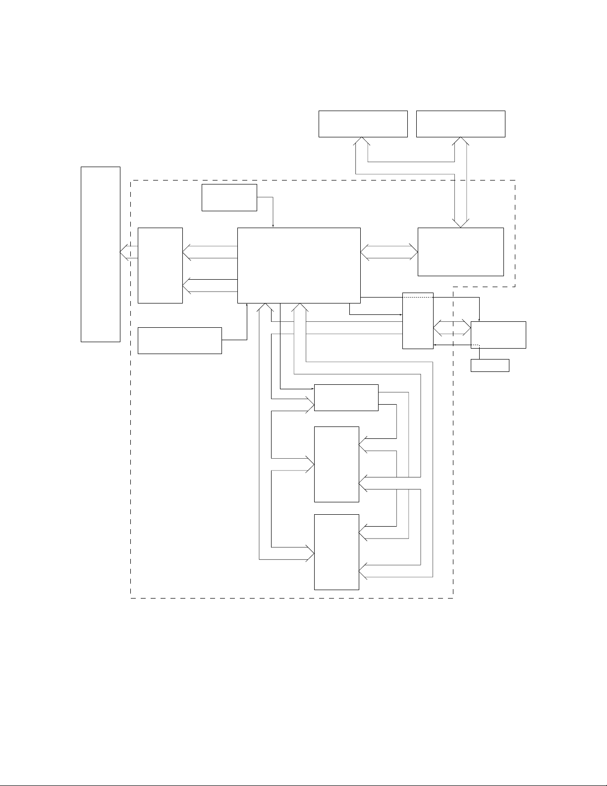
3-2. BLOCK DIAGRAM
PRINTER
M-190G
Head Drive Circuit
HA.A ~ HD.H
FD,RP,MD,DP
Power Supply Circuit
Reset Circuit
CUSTOMER DISPLAY
CPU
uPD78052GC-093-3B9
A8 ~ A15
ASTB
AD0 ~ AD7
enable
BUS Select Circuit
SH1019A
DI,DO,CLK,STB
Select address
AD0 ~ AD5
MAIN DISPLAY
SH101MA
Segment & Digit data
DISPLAY CONTROL
uPD16312GB-3B4
KEY Circuit
KC0 ~ KC4
Keynoard
Mode key
MAIN PCB E248-1
AD0 ~ AD7
AD0 ~ AD7
A0 ~ A7
ROM
A8 ~ A15
A0 ~ A7
RAM
A8 ~ A11
— 4 —
Page 7
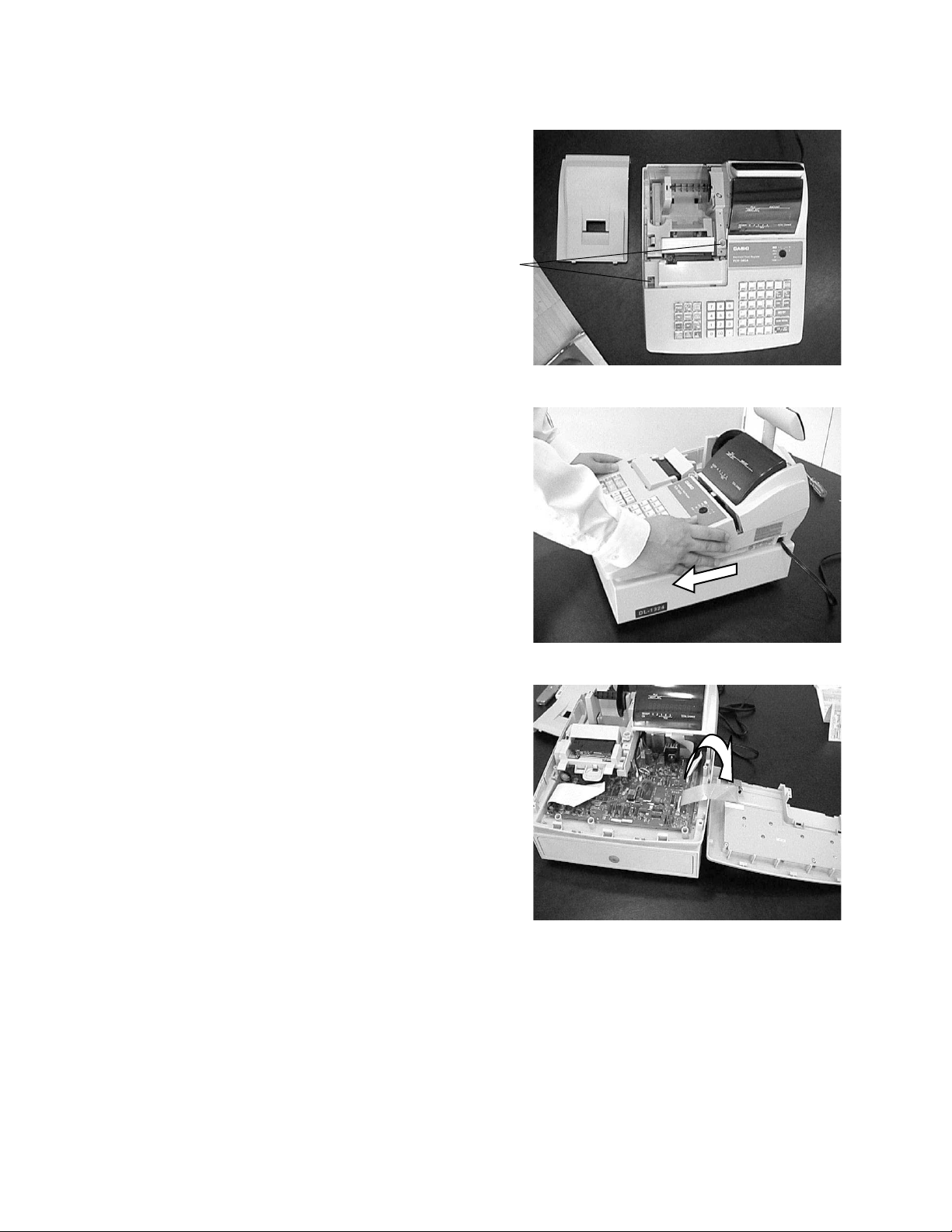
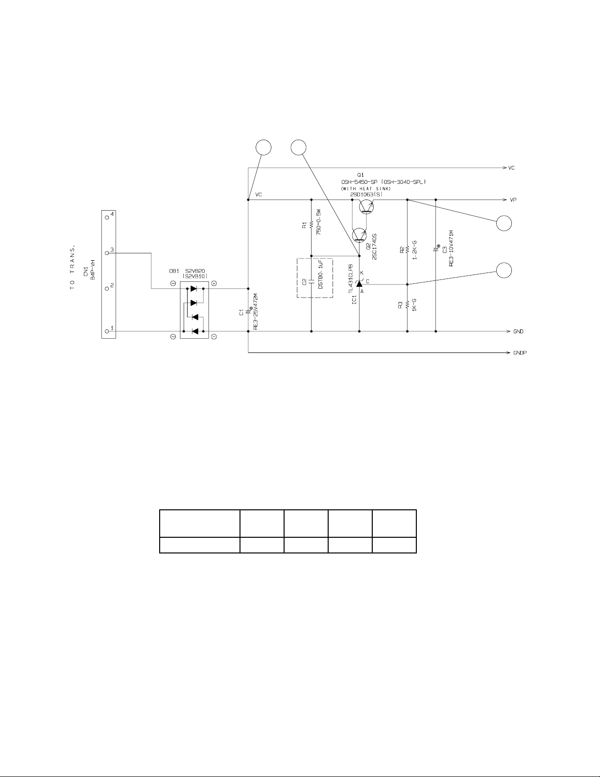
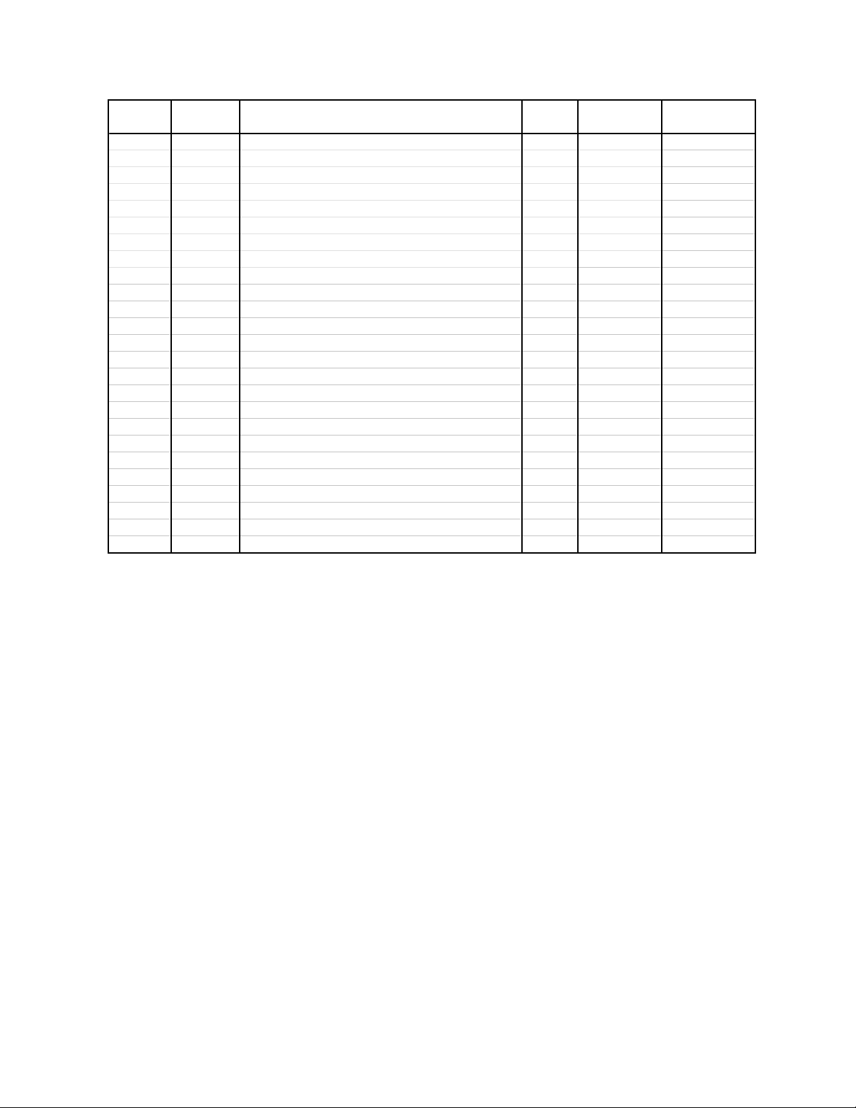
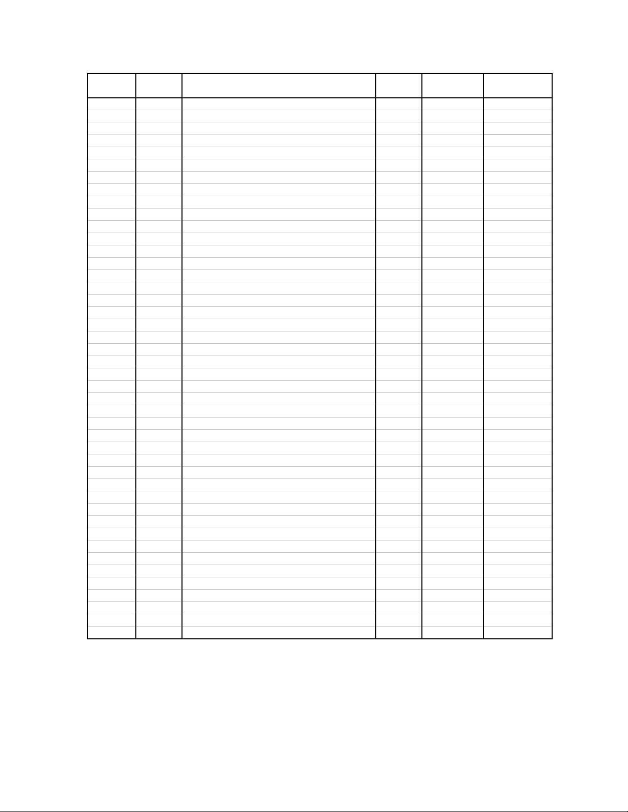
4. DISASSEMBLY
1. Open the printer cover.
Remove the 2 screws of the upper case.
2. Slide the upper case to the front side.
Remove the 2 screws.
3. Open upper case from the left side.
— 5 —
Page 8
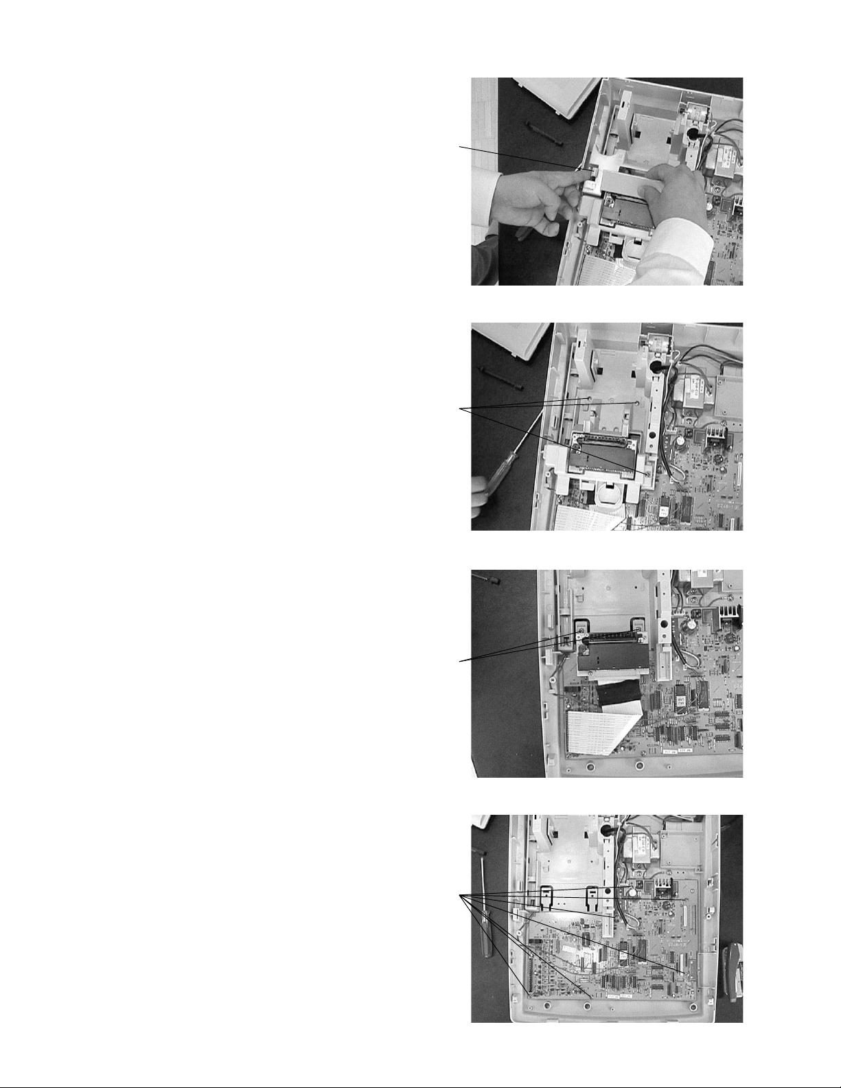
4. Release the hook them Remove the write side.
Hook
5. Release 3 screws to remove printer plastic
stand.
Remove the 3 screws
6. Release 2 screws to remove printer unit.
Remove the 2 screws
7. To remove the main PCB, release 7 screws.
Remove the 7 screws
— 6 —
Page 9
5. CIRCUIT EXPLANATION
5-1. Power supply circuit
A C
B
D
Q1: Power transistor
Q2: Voltage detection transistor
Voltage level at above check point (unit: V )
Measurement
position
ABCD
Voltage (V) 12.5V 5.3V 6.2V 2.47V
— 7 —
Page 10

5-2.CPU (uPD78052GC-159-3B9)
Pin No. Signal Description In/Out
1FB3 Not used — — —
2FB4 RAM bank 3 Out High High
3FB5 RAM bank 4 Out High High
4AVSS GND — GND GND
5PGM Not used — — —
6RAM Chip select signal for RAM Out High Low
7AVREF VDD — 5 V 5 V
8RXD Receive data In High High
9TXD Send data Out High High
10WD Winder motor drive signal Out Low Low
11DI Data signal from uPD16312 In Pulse High
12DO Data signal to uPD16312 Out Pulse High
13CLK Clock signal for uPD16312 Out Pulse High
14STB Data strobe signal for uPD16312 Out Pulse High
15KC0 Key common signal (KC0) Out Pulse High
16KC1 Key common signal (KC1) Out Pulse High
17KC2 Key common signal (KC2) Out Pulse High
18KC3 Key common signal (KC3) Out Pulse High
19AD0 Address / Data signal (AD0) In/Out Pulse High
20AD1 Address / Data signal (AD1) In/Out Pulse High
21AD2 Address / Data signal (AD2) In/Out Pulse High
22AD3 Address / Data signal (AD3) In/Out Pulse High
23AD4 Address / Data signal (AD4) In/Out Pulse High
24AD5 Address / Data signal (AD5) In/Out Pulse High
25AD6 Address / Data signal (AD6) In/Out Pulse High
26AD7 Address / Data signal (AD7) In/Out Pulse High
27A8 Address signal (A8) Out Pulse High
28A9 Address signal (A9) Out Pulse High
29A10 Address signal (A10) Out Pulse High
30A11 Address signal (A11) Out Pulse High
31A12 Address signal (A12) Out Pulse High
32A13 Address signal (A13) Out Pulse High
33VSS GND — GND GND
34A14 Address signal (A14) Out Pulse High
35A15 Address signal (A15) Out Pulse High
36INIT PAD2 status — — —
37VPP PAD1 status — — —
38DSR Data set ready signal In High High
39KC4 Key common signal (KC4) Out Pulse High
40RD Output enable signal of RAM/ROM (RD) Out Pulse High
41WR Write enable signal of RAM (WR) Out Pulse High
42RA14 Address signal of ROM (Bank 0) Out High High
43ASTB Latch enable for Address decoder (ASTB) Out Pulse Low
44KI12 Key input signal (KI12) In High High
45KI13 Key input signal (KI13) In High High
46RA16 Address signal of ROM (Bank2) Out High High
47RA15 Address signal of ROM (Bank 1) Out High High
48MD Motor drive signal of printer (MD) Out Low Low
49DRW Drawer drive signal (DRW) Out Low Low
50BUZ Buzzer signal (BUZZ) Out Low Low
51FD Paper feed signal of printer (FD) Out Low Low
52HD.A Head drive signal of printer (HD.A) Out Low Low
53HD.B Head drive signal of printer (HD.B) Out Low Low
54HD.C Head drive signal of printer (HD.C) Out Low Low
55HD.D Head drive si
gnal of printer (HD.D) Out Low Low
— 8 —
Status of
Power On
Status of
Power OFF
Page 11
Pin No. Signal Description In/Out
g
g
Status of
Power On
5 6 HD.E Head drive signal of printer (HD.E) O ut Low Low
5 7 HD.F Head drive signal of printer (HD.F) Ou t L ow Low
5 8 HD.G Head drive signal of printer (HD.G) Ou t L ow Low
5 9 HD.H Head drive signal of printer (HD.H) Out Lo w Low
6 0 RESET Reset signal (RESET) I n High High
6 1 DP Dot pulse form printer (DP) In Low High
6 2 RP Reset pulse from printer (RP) In High High
6 3 OFF Mode key status (OFF) Out High Lo w
6 4 PWD Power down signal (PWD) In Low High
6 5 RB0 Address signal for RAM (Bank 0) Out High High
6 6 RB1 Address signal for RAM (Bank 1) Out High High
6 7 RB2 Address signal for RAM (Bank 2) Out High High
6 8 VDD VDD — 5 V 5 V
6 9 X 2 System clock (5 MHz) In Pulse High
7 0 X 1 System clock (5 MHz) In Pulse High
7 1 IC GND — GND GND
7 2 XT2 Sub system clock (32.768 KHz) In Pulse Pulse
7 3 XT1 Sub system clock (32.768 KHz) In Pulse Pulse
7 4 AVDD VDD — 5 V 5 V
75 AVREF0 VCC — GND GND
7 6 BA T Low battery signal In High High
77 VPP.S VPP detection signal (VPP.S) In Lo w Low
7 8 FB0 Address signal of Fiscal ROM bank 0 Out High High
7 9 FB1 Address signal of Fiscal ROM bank 1 Out High High
8 0 FB2 Address si
nal of Fiscal ROM bank 2 Out HighHi
Status of
Power OFF
h
— 9 —
Page 12
y
)
5-3. Display controller (uPD16312GB-3B4)
Pin No. Signal Description In/Out
1 S W1 Not used (GND) — GND GND
2 S W2 Not used (GND) — GND GND
3 S W3 Not used (GND) — GND GND
4 S W4 Not used (GND) — GND GND
5 DOUT Data out signal to CPU Out High High
6 DIN Data in signal from CPU In Pulse High
7 VSS GND — GND GND
8 C LK Clock signal (CLK) In Pulse High
9 ST B Data strobe signal (STB) I n Pulse High
10 KEY1 Not used — — —
11 KEY2 Not used — — —
12 KEY3 Drawer sensor signal (DRW.S) I n High High
13 KEY4 VCC — 5 V 5 V
1 4 VDD VCC — 5 V 5 V
15 SEG1 Display segment signal (Sa) Ou t Pulse Low
16 SEG2 Display segment signal (Sb) Ou t Pulse Low
17 SEG3 Display segment signal (Sc) Ou t Pulse Low
18 SEG4 Display segment signal (Sd) Ou t Pulse Low
19 SEG5 Display segment signal (Se) Ou t Pulse Low
20 SEG6 Display segment signal (Sf) Out Pulse Low
21 SEG7 Display segment signal (Sg) Ou t Pulse Low
22 SEG8 Display segment signal (Sdp) Ou t Pulse Low
23 SEG9 Display segment signal (Str) Ou t Pulse Low
24 SEG10 Display segment common signal (Scom) Out Pulse Lo w
25 SEG11 Not used Low Low
26 SEG12 Not used Low Low
2 7 V EE Power for display (-VN) — -32 V -32 V
2 8 GRD10 Display digit signal (G10) Ou t Pulse Lo w
2 9 GRD9 Display digit signal (G9) Out Pulse L ow
3 0 GRD8 Display digit signal (G8) Out Pulse L ow
3 1 GRD7 Display digit signal (G7) Out Pulse L ow
3 2 GRD6 Display digit signal (G6) Out Pulse L ow
3 3 GRD5 Display digit signal (G5) Out Pulse L ow
3 4 GRD4 Display digit signal (G4) Out Pulse L ow
3 5 GRD3 Display digit signal (G3) Out Pulse L ow
3 6 GRD2 Display digit signal (G2) Out Pulse L ow
3 7 GRD1 Display digit signal (G1) Out Pulse L ow
3 8 VDD VCC — 5 V 5 V
39 LED4 Not used — Pulse Low
40 LED3 Not used — Pulse Low
41 LED2 Not used — Pulse Low
42 LED1 Not used — Pulse Low
4 3 V SS GND — GND GND
4 4 OSC S
stem clock (500 KHz
Status of
Power On
Status of
Power OFF
In Pulse Pulse
— 10 —
Page 13
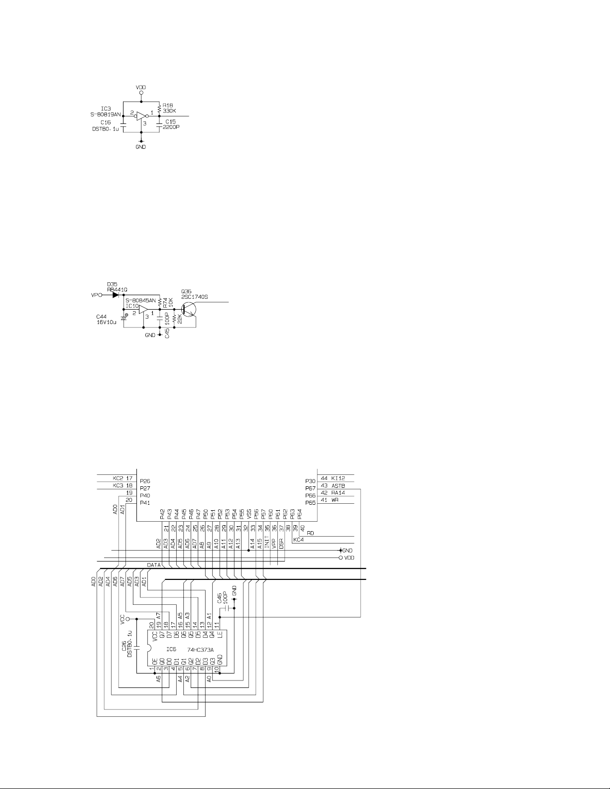
5-4. Initilize IC (Reset circuit)
VDD: Voltage of memory protection battery
To Pin No.60 of CPU
When the voltage level at Pin No.60 of CPU is not stabilized, CPU does not work properly in rare case.
Therefore, this machine uses the initialize IC for stabilizing the voltage.
Even the voltage level of VDD (Pin No.2) is changed, Pin No.1 of initilize IC outputs stabilized 5 volts.
When the VDD voltage become less than 1.9 V, the initialize IC send a reset signal to CPU.
5-5. Power down detection circuit (PWD)
To Pin No.64 of CPU
When the VP voltage become less than 4.8 V, the pin No.1 of IC5 become “Low” level.
Then,the transistor Q44 become OFF.
When Q44 become OFF, the voltage lebel of pin No.64 of CPU changes to “High” level from “Low”. Then,
CPU knows power failure.
5-6. Address latch circuit
CPU uses 8 port (AD0 ~ AD7) for
address bus and data bus.
To select the address, CPU use the
IC13.
CPU send the address to IC13, and
send ASTB signal at same time.
Then, IC13 store the address and
output the address immediately.
In this way, CPU select the address
and data signal.
— 11 —
Page 14
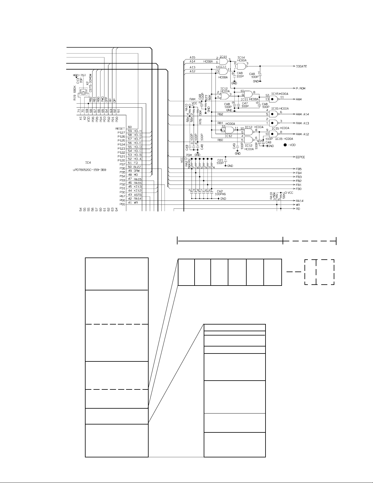
5-7. RAM / ROM bank selection circuit
This circuit is used for address decoder for memory.
0000
2000
Memory Map
Mask ROM
(16 K)
00001
000000
Bank
0
4000
EP ROM
6000
Common (16 K)
8000
EP ROM
Bank select area
A000
(16 K)
C000
RAM common area
(8 K)
E000
RAM BANK select
area (4 K)
F000
Outer I/O area
FA80
Internal RAM
(High speed access)
FFFF
— 12 —
RAM 256 K
00011
00010
Bank
Bank
1
KI signal port (F800,F801)
2
Bank
3
Buffer RAM 32 bytes
Internal RAM
(High speed access)
288 bytes
Internal RAM
(High speed access)
Short direct area
192 bytes
General purpose
register 32 bytes
Special function
register (SFR)
256 bytes
00100
Bank
4
00101
00110
Bank
5
F800
FAC0
FAE0
FD00
FE20
FEE0
FFF0
RAM 1 M
11101
Bank
29
Page 15
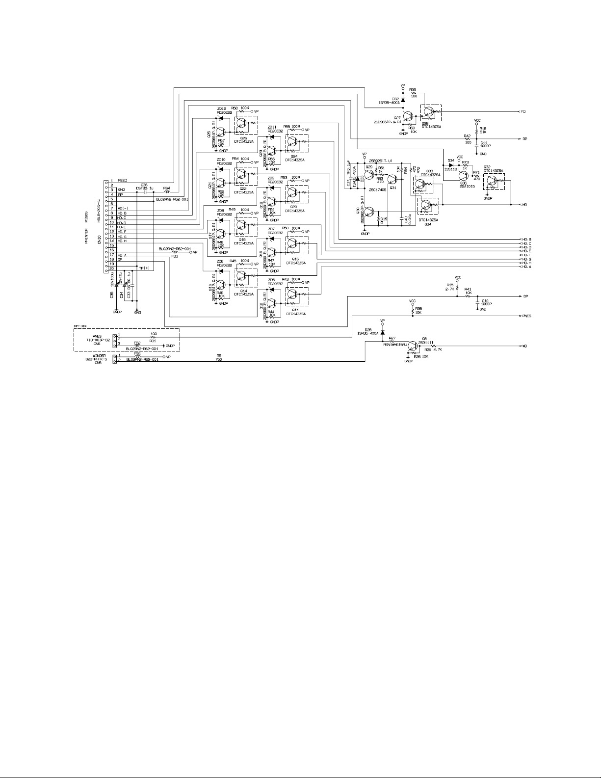
5-8. Head drive circuit for printer
TR5
TR4
TR3
TR1
TR2
Motor drive circuit
Normally, the transistor of motor drive circuit is followng condition.
TR1, TR2, TR5 : OFF
TR3, TR4 : ON
MD (-) signal : VP level
When the CPU want to rotate the motor, CPU change the MD signal to “High” from “Low”.
Then, TR1, TR2 and TR5 are become ON and MD (-) signal is become GND level,
and then motor is rotated.
Head drive circuit
When the CPU wants to print, CPU send “High” signal from HD.A ~ HD.H terminal.
This signal goes to printer unit, and then print.
RP: Reset pulse from printer
DP: Dot pulse from printer
— 13 —
Page 16

5-9. Power supply circuit for display
This circuit is making the power for display tube.
Voltage level: -VN Est. -31.2 V
VF1 - VF2 Est. AC4.85 V
— 14 —
Page 17
6. DIAGNOSTIC OPERATION
6-1. To start the diagnostic program
1. Set the mode switch to “OFF” position.
2. Pressing the “FEED” button and turn the mode switch to “PRG” position.
3. Release the “FEED” button.
4. Input “9999900000” and press “ST” (“#2” key).
5. Diagnostic program is executed.
6-2. Check item
The following test can be checked in the diagnostic test.
1. Key code test
2. Switch status test
3. Individul function test.
6-3. Operation of each test
1. Key code test
When pressing a key, the machine displays
the following key code.
HARD KEY CODE TABLE
FEED 055 051 789 046 040 034 028 022 016
058 054 050 456 045 039 033 027 021 015
057 053 049 123 044 038 032 026 020 014
056 052 C0011 012 043 037 031 025 019 013
“020” buttons are work for “#2” key.
DISPLAY
0 1 3
Hard key code
048 042 036 030 024 018
047 041 035 029 023 017
— 15 —
Page 18

2. Switch status test
Press “C” button, the switch status is appeared on the display.
[DISPLAY]
No display
No display
No display
No display
Low battery
L: Low battery
Nil: Battery OK
PAD2 status
1: Short
0: Open
PAD1 status
1: Short
0: Open
Always: 1
Drawer sensor
1: Close
0: Open
Mode switch status
1: PGM
2: RF
3: REG
4: CAL
5: X
6: Z
No display: OFF
— 16 —
Page 19

3. Individual function test
3-1. Series test
“Y” “X” “1” + “#2” key
Y: 0: Normal test
1: Execute next test even if an error happend at ROM check sum
X: 0: Autockecking of RAM capacity
1: 256 Kbit RAM test
2: 1 Mbit RAM test
Execute the following test in order.
1. Display test
2. Check sum test of EP-ROM
3. RAM test
4. Drawer open test
5. Printing test
6. Date and Time test
1. Display test (All segment light on)
2. Ckeck sum test of EP-ROM
Normal end Error end
ROM SUM OK
XX00: Check sum value XXXX : Check sum value
3. RAM test (Read/Write test)
Normal end receipt
256 Kbit RAM 1 Mbit RAM
Error end receipt
RAM 32K E R
4. Drawer open test
5. Printing test
YY: Bank
XXXX: Address
BBBBBBBBBBBBBBBBBBBBBBBB
ROM E R
RAM 128K R/W OK RAM 32K R/W OK
6. Date and Time test
Set the date and time as follows.
Date : 31 / 12 / 96 Time : 25:59
Then, issues a receipt and display the following character.
1 2. 3 4 5. 6 7 8. 9 0
— 17 —
Page 20

3-2. Print test
Input “Y” “X” “2” + “#2” key.
X: 0: Print the following character continuously.
Printing speed : 45 times / Min.
1: Print the following character, open the drawer and issue a receipt
Printing speed : 25 times / Min.
Drawer open : 5 times / Min.
Receipt issue : 5 times / Min.
Y: 0: No effect
1: Print the following character without waiting time. ( Continuously print )
To stop this test, press any key or turn the mode switch to “OFF” position.
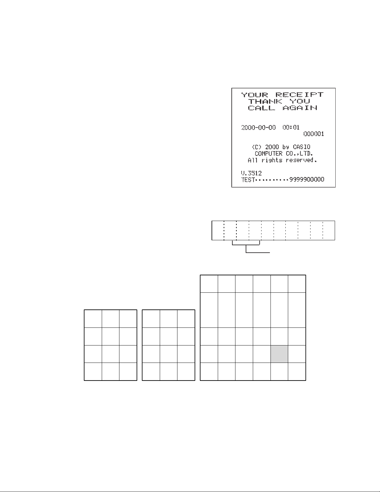
Printing sample:
3-3. RAM read only test
Input “X” “5” + “#2” key.
X: 0: Read the data from start to end address and issues receipt.
1: Read the data from start to end address continuously until power off.
Brink " - " signal on the display during checking.
Note: Be sure to execute the series test ( 1 + #2 ) before this test.
256 Kbit check receipt 1 Mbit check receipt
RAM 32K READ OK
Display
3-4. INIT OPERATION (To set a Factory Default setting)
Input “8” “6” + “#2” key.
BBBBBBBBBBBB
RAM 128K READ OK
The machine is executed a INIT operation according to PAD status.
Set the data and time to “0”.
(00-00-00, 00:00:00)
3-5. Voltage check for Memory protection battery
Input “7” + “#2” key.
Display the battery voltage.
To stop this test, press any key or turn the mode switch to “OFF” position.
XXX
X.XX: Voltage value
— 18 —
Page 21

3-6. All character print test
Input “8” + “#2” key.
“8” + “#2”: Pirnts all character on receipt once.
“1” “8” + “#2”: Prints all character on receipt continuously.
To stop this test, press any key or turn the mode switch to “OFF” position.
3-7. Time display test
Input “9” + “#2” key.
Display the time.
To stop this test, press any key or turn the mode switch to “OFF” position.
2 3 - 5 9 0 0
— 19 —
Page 22

3-8. RS232C port test
Input “2” “0” “7” + “#2” key.
Execute the RS232C loop back test continuously using loop back connector.
In case an error happens, the machine issues an error receipt then stop this test.
Test description: 1: Level check at DSR signal ( Low/High)
2: Send the data (05Ah) from TxD and receive it at RxD terminal.
To stop this test, turn the mode switch to “OFF” position.
Loop back connection:
TxD 2
RxD 3
DSR 6
Normal End Error End
232C OK
232C ER X
X: Error code
0: Time over
1: Over run error
2: Framing error
3: RXD line data error
4: DSR line receive error
6-4. To exit the diagnostic test
To escape the diagnostic test mode, execute “INITIALIZE (MAC) operation”.
— 20 —
Page 23

7. ERROR CODE
7-1. Operation error code
Error codes appear on display whenever you make a mistake during operation.
Error Code
E01
E08
E27
E31
E33
E35
E38
E94
Meaning
Mode switch position changed before finalization.
Registration without entering a clerk number. This
error appears only when the clerk control function
is activated.
Transaction cancel buffer full.
Finalization of a transaction attempted without
confirming the subtotal.
Finalize operation attempted without entering
amount tender.
Change amount over.
Read/reset operation without declaring cash in
drawer. This error appears only when this function
is activated.
Printer error.
Action
Return the mode switch to its original
setting and finalize the operation.
Enter a clerk number.
Finalize the transaction.
Press the
SUB
TOTAL
key.
Enter the amount tendered.
Require small money.
Perform money declaration.
Turn the power off, and remove jammed
paper from the printer.
Press
C
key and check the appropriate section of this manual for the operation you want to perform.
C/AC
— 21 —
Page 24

7-2. System lock code
The following error code appears on display and receipt when the machine is lock up.
Execute the Flag MAC or MAC operation to clear these errors.
Error code: Display: X - - - - - - - - -
Receipt: X ! ! ! ! ! ! ! ! ! ! ! ! ! ! ! ! ! !
X: Lock code
Error sample: 3 ! ! ! ! ! ! ! ! ! ! ! ! ! ! ! ! ! !
Error code Error Name Meaning
1 Sequential trap The machine try to write to accumulator when the CPU is
hung up.
2 Memory write error Error happens when the CPU write the data to memory.
3 Trap error Abnormal address
6 Timer error Interrupt timer error
7 Stack over Abnormal address or stack pointer has an error
0 Other error CPU executes wrong jump vector before detect 1, 3 and
6 error code.
— 22 —
Page 25

8. IC DATA
1
2
3
4
6
8
7
5
11
9
10
12
A1
B2
C3
G2A
G2B
G1
GND
( TOP VIEW )
Y7
VCC
Y0
Y1
Y2
Y4
Y3
Y6
Y5
16
15
14
13
SELECT
INPUTS
ENABLE
INPUTS
Y0
DATA
OUTPUTS
A
B
C
G2A
G2B
G1
Y1
Y0
Y3
Y4
Y5
Y6
Y7
1. TC74HC00AP
1
1A
2
1B
3
1Y
4
2A
5
2B
6
2Y
GND
7
3. TC74HC138
14
13
12
11
10
2. TC74HC08AP
VCC
4B
4A
4Y
3B
3A
9
3Y
8
1A
1B
1Y
2A
2B
2Y
GND
1
2
3
4
5
6
7
14
13
12
11
10
VCC
4B
4A
4Y
3B
3A
9
3Y
8
— 23 —
Page 26

4. TC74HC367AP
Output
Control G
116
1
215
1A
314
1Y
Vcc
Output
Control G
6A
5. TL431CLPB
TL431C
TIJxxxx
2
413
2A
2Y
512
3A
611
3Y
710
GND 9
8
6. TC74HC373AP
Output
Control
6Y
5A
5Y
4A
4Y
120
1Q
219
1D
318
Q
OE
D
G
Q
GOED
Vcc
8D
8Q
(R)
Vref
Vref 2.5 V
+
–
Anode (A)
Cathode (K)
2Q
417
2D
516
3Q
615
3D
714
4Q 13
8
912
4D
10
GND 11
Output
Control
DG
1D
1Q
D
G
OE
Q
Q
GOED
D
G
OE
Q
Q
2D
DG
2Q
D
G
OE
Q
Q
GOED
D
G
OE
Q
3Q
Q
Q
DG
3D
7D
7Q
6D
6Q
5D
5Q
Enable
G
4Q
Q
DG
4D
DG
5D
5Q
6Q
Q
DG
6D
7Q
Q
DG
7D
8Q
Q
DG
8D
Q
Enable
G
— 24 —
Page 27

7. S-80819AN-Z / S-80845AN-Z
(1) Nch open drain active low output
(2) CMOS active low output
S-808XX AX XX - XXX - T2
Tape spec. IC direction
Production short No.
Package No.
NP: SC-82AB
MP: SOT-23-5
UP: SOT-89-3
Y: TO-92
Output
N: Nch open drain (Active "L")
L: CMOS (Active "L")
Detection Voltage X 10 times
— 25 —
Page 28

9. PCB LAYOUT
— 26 —
Page 29

10. CIRCUIT DIAGRAMS
MODEL : PCR-365A (EX-248AC)
CONTENTS
1. LOCATION OF PRINTED CIRCUIT BOARD .................................................................. 28
2. MAIN PCB CIRCUIT........................................................................................................ 29
2-1. MAIN PCB CIRCUIT (1/7) ........................................................................................ 29
2-2. MAIN PCB CIRCUIT (2/7) ........................................................................................ 30
2-3. MAIN PCB CIRCUIT (3/7) ........................................................................................ 31
2-4. MAIN PCB CIRCUIT (4/7) ........................................................................................ 32
2-5. MAIN PCB CIRCUIT (5/7) ........................................................................................ 33
2-6. MAIN PCB CIRCUIT (6/7) ........................................................................................ 34
2-7. MAIN PCB CIRCUIT (7/7) ........................................................................................ 35
3. LED DISPLAY.................................................................................................................. 36
3-1. MAIN DISPLAY ........................................................................................................ 36
3-2. REAR DISPLAY ....................................................................................................... 37
CE-250 (EX-248BC)
CE-200 (EX-248CC)
4. KEYBOARD..................................................................................................................... 38
5. POWER SUPPLY CIRCUIT ............................................................................................ 39
6. BATTERY ........................................................................................................................ 40
7. MOTOR ........................................................................................................................... 41
— 27 —
Page 30

1
2
3
4
5
6
7
8
EX240698
LOCATION OF PRINTED
CIRCUIT BOARDS
Description: Board No. Drawing No.
BCDEFGHI JKA
1
2
3
4
5
6
7
8
BCDEFGHI JKA
— 28 —
Page 31

1
2
3
4
5
6
7
8
E248-1 (1/7) E240699-1
MAIN PCB
Description: Board No. Drawing No.
BCDEFGHI JKA
BCDEFGHI JKA
1
2
3
4
5
6
7
8
— 29 —
Page 32

1
2
3
4
5
6
7
8
MAIN PCB E248-1 (2/7) E240699-2
Description: Board No. Drawing No.
BCDEFGHI JKA
BCDEFGHI JKA
1
2
3
4
5
6
7
8
— 30 —
Page 33

1
2
3
4
5
6
7
8
MAIN PCB E248-1 (3/7) E240699-3
Description: Board No. Drawing No.
BCDEFGHI JKA
BCDEFGHI JKA
1
2
3
4
5
6
7
8
— 31 —
Page 34

1
2
3
4
5
6
7
8
MAIN PCB E248-1 (4/7) E240699-4
Description: Board No. Drawing No.
BCDEFGHI JKA
BCDEFGHI JKA
1
2
3
4
5
6
7
8
— 32 —
Page 35

1
2
3
4
5
6
7
8
MAIN PCB E248-1 (5/7) E240699-5
Description: Board No. Drawing No.
BCDEFGHI JKA
BCDEFGHI JKA
1
2
3
4
5
6
7
8
— 33 —
Page 36

1
2
3
4
5
6
7
8
MAIN PCB E248-1 (6/7) E240699-6
Description: Board No. Drawing No.
BCDEFGHI JKA
BCDEFGHI JKA
1
2
3
4
5
6
7
8
— 34 —
Page 37

1
2
3
4
5
6
7
8
MAIN PCB E248-1 (7/7) E240699-7
Description: Board No. Drawing No.
BCDEFGHI JKA
BCDEFGHI JKA
1
2
3
4
5
6
7
8
— 35 —
Page 38

Description: Board No. Drawing No.
MAIN DISPLAY E248-E2-1 E441107
— 36 —
Page 39

Description: Board No. Drawing No.
REAR DISPLAY E248-E2-2 E441108
— 37 —
Page 40

1
2
3
4
5
6
7
8
E266-E3-1 E240700
KEYBOARD
Description: Board No. Drawing No.
BCDEFGHI JKA
BCDEFGHI JKA
1
2
3
4
5
6
7
8
— 38 —
Page 41

1
2
3
4
5
6
7
8
E341071
POWER SUPPLY
Description: Board No. Drawing No.
BCDEFGHI JKA
1
2
3
4
5
6
7
8
BCDEFGHI JKA
— 39 —
Page 42

Description: Board No. Drawing No.
BATTERY E441109
— 40 —
Page 43

Description: Board No. Drawing No.
MOTOR E441110
— 41 —
Page 44

11. PARTS LIST
MODEL : PCR-365A (EX-248AC)
CE-250 (EX-248BC)
CE-200 (EX-248CC)
CONTENTS
Exploded view................................................................................................... 43
1. Main PCB block E248-1 ass’y.................................................................... 45
2. Main display block E248-E2-1....................................................................46
3. Customer display block E248-E2-2............................................................ 46
4. Button block ...............................................................................................46
5. Power supply block ....................................................................................47
6. Upper case block .......................................................................................48
7. Lower case block .......................................................................................48
8. Printer block ...............................................................................................48
9. Others ........................................................................................................48
10.Cash drawer (DL-1324).............................................................................49
11.Printer (M-190G)........................................................................................51
Notes:
1. Prices and specifications are subject to change without notice.
2. As for order / supply of spare parts, refer to the "GUIDEBOOK for Spare Parts Supply", a separate
publication.
3. The numbers in item column correspond to the same numbers in drawing.
4. MARKS:
Q: Quantity used per unit
R: Rank
A: Essential
B: Stock recommended
C: Less recommended
X: No stock recommended
— 42 —
Page 45

50
49
57
8
7
39
4
38
5
6
55
53
51
56
52
54
41
47
48
45
36
43
44
42
46
37
35
40
2
58
Keyboard
3
E248-1 ass’y
— 43 —
1
Drawer
Page 46

32
Keyboard Block
33
16
14
11
18
22
17
15
12
13
9
9
8
6
7
5
3
4
2
.
1
00
0
10
20
21
19
30
27
28
29
34
23
24
25
26
31
— 44 —
Page 47

PARTS PRICE LIST
N Item Code No. Parts Name Specification
Price code
Rank
PCR-365A CE-250 CE-200
1. Main PCB block
N 1 10015651 PCB ASSY SET/E248-1, E248-E2-1 E140345*1 1 1 1
DX
A
and E248-E2-2
F1 30007777 FUSE 230.600 1 1 1
AE
A
IC1 21207349 IC/LINEAR TL431CLPB 1 1 1
AG
A
IC10 21120837 IC/RESET S-80845ANY-Z 1 1 1
AB
A
IC11,13 21051218 IC/MOS TC74HC08AP 2 2 2
AC
A
IC12,14,15 21051008 IC/MOS TC74HC00AP 3 3 3
AC
A
IC18 21010189 IC/MOS TC74HC138AP 1 1 1
AE
A
IC2 20061326 LSI UPD16312GB-3B4 1 1 1
AX
A
IC3 21120840 IC/RESET S-80819ANY-Z 1 1 1
AB
A
N IC4 10024616 LSI UPD78052GC-159-3B9 1 1 1
CE
A
IC6 21051169 IC/MOS TC74HC373AP 1 1 1
AG
A
IC7 20061648 LSI M27C512-10/12F1 1 1 1
BD
A
IC8 20061701 LSI TC55257DPL-70L/85L 1 1 1
AT
A
IC9,16,17 21120035 IC/MOS TC74HC367AP 3 3 3
AF
A
X1 25203445 OSCILLATOR/CRYSTAL C-002RX(M90-76) 1 1 1
AD
A
X2 24088261 LOCK/CERAMIC CST5.00MGW 1 1 1
AD
A
D1,D28,D32,D33 23153128 DIODE 1SR35-400AT-82 4 4 4
AA
B
D29,D30 23153134 DIODE SB10-04A3-BT 2 2 2
AB
B
D31 23153095 DIODE/SHOTTKY RB721Q-40T-77 1 1 1
AA
B
D34 23153131 DIODE 1SS118TD 1 1 1
AA
B
D35 23902828 DIODE RB441Q-40T-77 1 1 1
AA
B
D3-D5,D7-D26 23153132 DIODE 1SS133T-77 23 23 23
AA
B
D6 23153133 DIODE 1SS244T-77 1 1 1
AA
B
DB1
23152857 BRIDGE/DIODE S2VB20
1 1 1
AF
B
DCS1
30007623 CONVERTER/DC-DC DCS-298
1 1 1
AR
B
N FB1,3,4
30006335
INDUCTOR
BL02RN2-R62-001
3 3 3
AB
B
Q1
22501554
TRANSISTOR
2SD1063(R,S)
1 1 1
AN
B
23,25,27,30
Q2,5,31,36
22501330
TRANSISTOR
2SC1740S(QRSE)TP
4 4 4
AA
B
Q29
22107186
TRANSISTOR
2SB926(T,U)-AA
1 1 1
AC
B
Q3
22501309
TRANSISTOR
2SD1804(T)
1 1 1
AF
B
N Q35
22501633
TRANSISTOR
2SA1015(0.Y.GR)-TP
1 1 1
AA
B
Q4
22501323
TRANSISTOR
2SA933AS(QRS)TP
1 1 1
AA
B
Q6
22304135
TRANSISTOR
2SD1853-AA
1 1 1
AC
B
Q8
22303902
TRANSISTOR
2SD1111-AA
1 1 1
AC
B
ZD1
23152661 DIODE/ZENER RD36EB1-T1
1 1 1
AA
B
ZD2
23153112 DIODE/ZENER RD33EB1-T1
1 1 1
AA
B
ZD3
23153109 DIODE/ZENER RD5.6EB2-T1
1 1 1
AA
B
ZD5-12
23152836 DIODE/ZENER RD20EB2-T1
8 8 8
AA
B
BZ1
32402089 BUZZER PKM22EPT-2001
1 1 1
AE
C
C1
28072658 CAPACITOR/ELECTROLYTIC RE3-25V472M
1 1 1
AL
C
C14,34
28073099 CAPACITOR/ELECTROLYTIC RE2-10V470MMA-T2
2 2 2
AA
C
C19
28073582 CAPACITOR/ELECTROLYTIC RE3-6.3V472M
1 1 1
AE
C
C3,18
28072294 CAPACITOR/ELECTROLYTIC RE3-10V471M-T2
2 2 2
AB
C
C35
28072707 CAPACITOR/ELECTROLYTIC RE3-16V101M-T2
1 1 1
AA
C
C44
28072847 CAPACITOR/ELECTROLYTIC RE2-16V100MMA-T2
1 1 1
AA
C
C7
28073575 CAPACITOR/ELECTROLYTIC RE2-50V101M-T2
1 1 1
AB
C
C7,9,10
28451134 CAPACITOR/MODULE CNB4X101K
3 3 3
AC
C
CA1
28450056 CAPACITOR/MODULE CNB6X221K
1 1 1
AC
C
CA2
28450182 CAPACITOR/MODULE CNB6X101K
1 1 1
AC
C
CA3-6,8,11
28450168 CAPACITOR/MODULE CNB8X101K
6 6 6
AD
C
CN1
35802371 CONNECTOR B4P-VH
1 1 1
AB
C
CN10
35107631 CONNECTOR HBLB20S-1J
1 1 1
AE
C
CN2
35003355 CONNECTOR IL-G-3P-S3T2-E
1 1 1
AA
C
CN4,11
35015404 CONNECTOR 52045-2445
2 2 2
AD
C
CN5
35016244 CONNECTOR B2B-PH-K-S
1 1 1
AA
C
CN8
35005845 CONNECTOR B3B-PH-K-S
1 1 1
AA
C
FT1
28073619 FILTER/EMI DSS310H-55B222M250
1 1 1
AB
C
IC7
36350024 SOCKET/IC DILB28P-8JK
1 1 1
AC
C
RA1
26522274 RESISTOR/CHIP NETWORK RGLD4X222J
1 1 1
AA
C
RA2,6,7,11
26522288 RESISTOR/CHIP NETWORK RGLD6X563J
4 4 4
AA
C
RA3-5,8
26521350 RESISTOR/CHIP NETWORK RGLD8X563J
4 4 4
AB
C
RA9,10,12
26522281 RESISTOR/CHIP NETWORK RGLD4X563J
3 3 3
AA
C
C10,11
CAPACITOR/CERAMIC RT-HE50TKYB102K
2 2 2
NOT SUPPLY
X
C12
CAPACITOR/CERAMIC RT-HE40TKCH120J
1 1 1
NOT SUPPLY
X
C13
CAPACITOR/CERAMIC RT-HE40TKCH150J
1 1 1
NOT SUPPLY
X
Q'ty
Q10,11,14,16,18,20,
Q12,13,15,17,19,21,
22501635 TRANSISTOR DTC143ZSA-TP 13 13 13 AA B
22305261 TRANSISTOR 2SD965(P.Q.R)-TA 10 10 10 AB B
- 45 -
Page 48

N Item Code No. Parts Name Specification
Price code
Rank
PCR-365A CE-250 CE-200
Q'ty
C16,17,20,26,31,33,
36,50-54
C24,43
CAPACITOR/CERAMIC RT-HE12TKYB103K
2 2 2
NOT SUPPLY
X
C28
CAPACITOR/CERAMIC RT-HE40TKYB221K
1 1 1
NOT SUPPLY
X
C5,15
CAPACITOR/CERAMIC RT-HE60TKYB222K
2 2 2
NOT SUPPLY
X
C6
CAPACITOR/CERAMIC RT-HE40TKYB471K
1 1 1
NOT SUPPLY
X
C8,29,30,37
CAPACITOR/FILM AMZV0050K1040200
4 4 4
NOT SUPPLY
X
42,45-49
R1
RESISTOR R-50XT-24J751
1 1 1
NOT SUPPLY
X
R10
RESISTOR R-50XT-24J101
1 1 1
NOT SUPPLY
X
R12
RESISTOR RD1/4WT-24Y201J
1 1 1
NOT SUPPLY
X
R14,35,67,75
RESISTOR RD1/4WT-24Y223J
4 4 4
NOT SUPPLY
X
R15
RESISTOR RD1/4WT-24Y272J
1 1 1
NOT SUPPLY
X
R16,37
RESISTOR RD1/4WT-24Y513J
2 2 2
NOT SUPPLY
X
R18
RESISTOR RD1/4WT-24Y334J
1 1 1
NOT SUPPLY
X
R19
RESISTOR RD1/4WT-24Y684J
1 1 1
NOT SUPPLY
X
R2
RESISTOR RD1/4WT-24Y122G
1 1 1
NOT SUPPLY
X
R22
RESISTOR RD1/4WT-24Y105J
1 1 1
NOT SUPPLY
X
R24
RESISTOR RD1/4WT-24J104J
1 1 1
NOT SUPPLY
X
R25,66
RESISTOR RD1/4WT-24Y472J
2 2 2
NOT SUPPLY
X
R27
RESISTOR RSN1WMG15RJ
1 1 1
NOT SUPPLY
X
R29
RESISTOR RD1/4WT-24Y222J
1 1 1
NOT SUPPLY
X
R3
RESISTOR RD1/4WT-24Y102G
1 1 1
NOT SUPPLY
X
R39,76-79
RESISTOR RD1/4WT-24Y563J
5 5 5
NOT SUPPLY
X
R4
RESISTOR CRH100-FH11J-2R2
1 1 1
NOT SUPPLY
X
R40,61,62,68,73
RESISTOR RD1/4WT-24Y102J
5 5 5
NOT SUPPLY
X
R5
RESISTOR
RD1/4WT-24Y751J 1 1 1
NOT SUPPLY
X
R63,71,72
RESISTOR RD1/4WT-24Y471J
3 3 3
NOT SUPPLY
X
R70
RESISTOR RD1/4WT-24Y221J
1 1 1
NOT SUPPLY
X
SCREW 3X8 ZMC-3.....
7 7 7
NOT SUPPLY
X
2. Main Display block
2 PCB ASSY/E248-E2-1 (Order by Main PCB) 1 1 1
NOT SUPPLY
X
DISP1
24088226 TUBE/DISPLAY
SH101MA
1 1 1
BP
B
CUSHION/DISPLAY
E412177-1
2 2 2
NOT SUPPLY
X
CN1
35015404 CONNECTOR
52045-2445
1 1 1
AD
C
N CN2
10030171 CONNECTOR
52806-1210
1 1 1
AC
C
N CN3
10030170 CONNECTOR
52806-1010
1 1 1
AC
C
3
62480508 CABLE/FFC JOINT E E247 E440442-1
1 1 1
AK
C
30008040 CORE/FERRITE SSC-40-12
1 1 1
AF
C
3. Customer Display block
4 PCB ASSY/E248-E2-2 (Order by Main PCB) 1 1 1
NOT SUPPLY
X
DISP1
24088233 TUBE/DISPLAY
SH1019A
1 1 1
BM
B
CUSHION/DISPLAY
E440189-4
2 2 2
NOT SUPPLY
X
N CN1
10030157 CONNECTOR
52807-1210
1 1 1
AA
C
N CN2
35022620 CONNECTOR
52807-1010
1 1 1
AA
C
5
62481476 CABLE/FFC JOINT E E445 E440657-5
1 1 1
AU
C
6
62481475 CABLE/FFC JOINT D E445 E440657-4
1 1 1
AU
C
30008041 CORE/FERRITE SSC-33.5-12
AE
7
62481274 CASE/REAR DISPLAY E240511-1
1 1 1
AY
C
N 8
10027092 PLATE/REAR DISPLAY E240512A-6
1 1 1
AT
B
62481698 PLATE/INSULATION E440781-1
1 1 1
AB
C
4. Button block
9
62213988 CAP/L E210964-1
3 3 3
AB
C
10
62214025 CAP/S E311103-1
42 42 42
AA
C
11
62457250
BUTTON/1
E311792-1
1 1 1
AB
C
12
62457260
BUTTON/2
E311792-2
1 1 1
AB
C
13
62457270
BUTTON/3
E311792-3
1 1 1
AB
C
14
62457280
BUTTON/4
E311792-4
1 1 1
AB
C
15
62457290
BUTTON/6
E311792-5
1 1 1
AB
C
16
62457300
BUTTON/7
E311792-6
1 1 1
AB
C
17
62457310
BUTTON/8
E311792-7
1 1 1
AB
C
18
62457320
BUTTON/9
E311792-8
1 1 1
AB
C
19
62457330
BUTTON/0
E311792-9
1 1 1
AB
C
20
62457340
BUTTON/.
E311792-10
1 1 1
AB
C
CAPACITOR/CERAMIC RT-DSTB90TKYR104K 12 12 12 NOT SUPPLY X
C9,21-23,25,27,40-
R7,23,3234,38,42,43,45,49,5
R8,9,11,17,26,36,41
,44,4648,51,52,56,57,60,6
CAPACITOR/CERAMIC RT-HE40TKYB101K 14 14 14 NOT SUPPLY X
RESISTOR RD1/4WT-24Y101J 17 17 17 NOT SUPPLY X
RESISTOR RD1/4WT-24Y103J 18 18 18 NOT SUPPLY X
- 46 -
Page 49

N Item Code No. Parts Name Specification
Price code
Rank
PCR-365A CE-250 CE-200
Q'ty
21
62457350
BUTTON/00
E311792-11
1 1 1
AB
C
22
62457360
BUTTON/5
E311116-4
1 1 1
AB
C
23
62467768 BUTTON/L E210963A-4
3 3 3
AD
B
24
62467810 BUTTON/S E311101A-4
54 54 54
AA
B
25
62473830 SPRING/COIL E411104A-1
3 3 3
AA
B
26
62480990 RUBBER/KEY E411877A-1
57 57 57
AA
B
27
62473837 SPRING/COIL E411104A-2
5 5 5
AA
B
28
62476371 SHEET/COMMON E340398-1
1 1 1
AM
B
29
62476364 SPACER E340397-1
1 1 1
AD
C
30
62476357 FPC E240323-1
1 1 1
BK
B
31
CHASSIS/KEY BOARD E340412A-1
1 1 1
NOT SUPPLY
X
32
61924970 SWITCH SUB ASSY/MODE KEY E311944*1
1 1 1
BL
B
N 33
10021657 PLATE/MODE KEY E440460-13
1 1 1
AG
C
N 33 10027111 PLATE/MODE KEY E248BC E440460-14 1
AG
C
N 33 10027112 PLATE/MODE KEY E248CC E440460-15 1
AG
C
N 34
10021806 FRAME/BUTTON E140378-1
1 1 1
BF
C
N FEED
10021648 PLATE/S E240526-93
1 1 1
AA
C
N %
10021639 PLATE/S E341037-28
1 1 1
AA
C
N -
10021641 PLATE/S E341037-30
1 1 1
AA
C
POST
RECEIPT/EXCHG
N #/NS 10017346
PLATE/S
E240526-66 1 1 1
AA
C
N PRICE
10021640 PLATE/S E341037-29
1 1 1
AA
C
N RF
10021642 PLATE/S E341037-31
1 1 1
AA
C
CORR/CANCEL
N OPEN/CLK#
10021638 PLATE/S E341037-27
1 1 1
AA
C
N PLU/S.DEPT
10029194 PLATE/S E240526A-99
1 1 1
AA
C
X/FOR/DATE TIME
N C(C/AC)
62481413 PLATE/S E240526-11
1 1 1
AA
C
N DEP1
10021611 PLATE/S E341037-1
1 1 1
AA
C
N DEP2
10021612 PLATE/S E341037-2
1 1 1
AA
C
N DEP3
10021613 PLATE/S E341037-3
1 1 1
AA
C
N DEP4
10021614 PLATE/S E341037-4
1 1 1
AA
C
N DEP5
10021615 PLATE/S E341037-5
1 1 1
AA
C
N DEP6
10021616 PLATE/S E341037-6
1 1 1
AA
C
N DEP7
10021650 PLATE/S E240526-95
1 1 1
AA
C
N DEP8
10021617 PLATE/S E341037-7
1 1 1
AA
C
N DEP9
10021618 PLATE/S E341037-8
1 1 1
AA
C
N DEP10
10021619 PLATE/S E341037-9
1 1 1
AA
C
N DEP11
10021621 PLATE/S E341037-10
1 1 1
AA
C
N DEP12
10021622 PLATE/S E341037-11
1 1 1
AA
C
N DEP13
10021651 PLATE/S E240526-96
1 1 1
AA
C
N DEP14
10021623 PLATE/S E341037-12
1 1 1
AA
C
N DEP15
10021624 PLATE/S E341037-13
1 1 1
AA
C
N DEP16
10021625 PLATE/S E341037-14
1 1 1
AA
C
N DEP17
10021626 PLATE/S E341037-15
1 1 1
AA
C
N DEP18
10021627 PLATE/S E341037-16
1 1 1
AA
C
N DEP19
10021652 PLATE/S E240526-97
1 1 1
AA
C
N DEP20
10021628 PLATE/S E341037-17
1 1 1
AA
C
N DEP21
10021629 PLATE/S E341037-18
1 1 1
AA
C
N DEP22
10021630 PLATE/S E341037-19
1 1 1
AA
C
N DEP23
10021631 PLATE/S E341037-20
1 1 1
AA
C
N DEP24
10021632 PLATE/S E341037-21
1 1 1
AA
C
N DEPT SHIFT
10029193 PLATE/S E240526A-98
1 1 1
AA
C
N RC/T/S1
10021634 PLATE/S E341037-23
1 1 1
AA
C
N CH
10021636 PLATE/S E341037-25
1 1 1
AA
C
N RECEIPT ON/OFF
10021633 PLATE/S E341037-22
1 1 1
AA
C
N PD/T/S2
10021635 PLATE/S E341037-24
1 1 1
AA
C
N CHK
10021637 PLATE/S E341037-26
1 1 1
AA
C
N MD/ST
10021653 PLATE/L E240527-25
1 1 1
AA
C
N SUB TOTAL
10021646 PLATE/L E341038-1
1 1 1
AA
C
N CA/AMT TEND(=)
10021647 PLATE/L E341038-2
1 1 1
AA
C
SCREW 3X8 ZMC-3 6
6 6
NOT SUPPLY
X
5. Power supply block
N 35
10024685 TRANSFORMER TE-248-E1D
1 1 1
CN
A
36
10023027 CODE/POWER PS204-A
1 1 1
AR
C
37
55300526 TERMINAL CE2
2 2 2
AA
C
TIE/INSULOCK T-18S
1 1 1
NOT SUPPLY
X
SCREW 4X8 ZMC-3
1 1 1
NOT SUPPLY
X
LABEL/FUSE WARNING E440881-1
1 1 1
NOT SUPPLY
X
N
ERR.
N
10021644 PLATE/S E341037-33 1 1 1 AA C
10021645 PLATE/S E341037-34 1 1 1 AA C
N
10021643 PLATE/S E341037-32 1 1 1 AA C
- 47 -
Page 50

N Item Code No. Parts Name Specification
Price code
Rank
PCR-365A CE-250 CE-200
Q'ty
6. Upper case block
N 38
10015632 CASE/UPPER E140341-1
1 1 1
AW
C
N 39
10015633 CASE/DISPLAY E140342-1
1 1 1
AY
C
40
62202505 BUSH/DISPLAY E231 E310377-1
1 1 1
AC
C
TIE/CABLE T-30L
1 1 1
NOT SUPPLY
X
SCREW 3X20 ZMC-3
2 2 2
NOT SUPPLY
X
7. Lower case block
41
62476385 CASE/LOWER E245A E140118-1
1 1 1
BU
C
NUT SB-3001
1 1 1
NOT SUPPLY
X
42
32003672 MOTOR MXN-13FB12F
1 1 1
AV
B
43
62316837 RUBBER/WINDER E222 E410716A-1
1 1 1
AB
B
44
61910122 CONNECTOR ASSY/MOTOR E311086*1
1 1 1
AP
C
45
62480887 CONNECTOR ASSY/BATTERY E340620*1
1 1 1
AC
C
46
60006091 SPRING/BATTERY G67 A43656-1
1 1 1
AA
C
47
63224499 SPRING/BATTERY A-G55 A42606-1
1 1 1
AA
C
48
62478821 COVER/BATTERY E340406-1
1 1 1
AL
C
8. Printer block
N 49
10015631 COVER/PRINTER E248 E140343-1
1 1 1
BE
C
50
62313668 CUTTER/PRINTER E42592A-1
1 1 1
AB
C
N 51
10015630 STAND/PRINTER FIXING E140344-1
1 1 1
AS
C
52
10003305 PRINTER M-190G(071)
1 1 1
DA
A
SCREW 2.3X5 NI
3 3 3
NOT SUPPLY
X
N 53
10015628 HOLDER/PRINTER E248 E340977-1
1 1 1
AI
C
N 54
10022577 CABLE/JOINER H-E248 E440443-3
1 1 1
AO
C
55
62480298 TABLE/WRITING E140175-1
1 1 1
AN
C
56
62214029 SPOOL/PAPER HOLDING E227 E411393-1
1 1 1
AE
C
57
62461830 PULLEY/WIND E226 E311860-1
1 1 1
AJ
C
9. Others
62480911 KEY SET SUB ASSY E312046A*3 1 1 1
AF
B
SCREW 4X8 ZMC-3 2 2 2
NOT SUPPLY
X
WASHER 4 ZMC-3 3 3 3
NOT SUPPLY
X
SCREW 3X8 ZMC-3 3 3 3
NOT SUPPLY
X
SCREW 3X8 ZMC-3 1 1 1
NOT SUPPLY
X
SCREW 3X8 NI 1 1 1
NOT SUPPLY
X
CUSHION E248 E441127-1 1 1 1
NOT SUPPLY
X
SCREW 4X85 ZMC-3 1 1 1
NOT SUPPLY
X
WASHER 4X9X0.8 ZMC-3 1 1 1
NOT SUPPLY
X
SCREW 4X8 ZMC-3 2 2 2
NOT SUPPLY
X
- 48 -
Page 51

10. Cash drawer (DL-1324)
25
26
24
11
19
17
18
16
23
22
× 2
20
× 4
5
× 4
4
× 3
12
2
8
14
× 2
3
15
× 2
7
× 2
6
21
× 5
1
10
13
× 4
9
— 49 —
Page 52

NItem Code No. Parts Name Specification QtyPrice CodeRank
N 1 10022673 DRAWER ASSY E240689*1 1 C
N 2 10022665 CASE/COIN E240644-1 1 B
3 62466571 PLATE /BILL HOLDER FIXING E311873-1 1 AS C
4 62481217 HOLDER/BILL E340725-1 4 AA A
5 62465220 SPRING/BILL HOLDER E412160-1 4 AB A
SCREW 3X8 ZMC-3 3 X
6 55000878 ROLLER/DERLIN DR-19B2 2 AP A
7 51501643 NUT 6... 2 AA X
8 51501648 RIVET/FLAT D5X26 1 AA X
9 55801452 CS RING CSTW-5 1 AA X
10 62464960 CYLINDER LOCK ASSY E311950*1 1 AT C
11 62465000 DRAWER KEY SUB ASSY E412062*1 1 AG C
12 62466585 PLATE/ PARTITION E340010-5 3 AC B
N 13 10022666 PLATE/COIN PARTITION E340966-1 4 B
14 62481222 CASE/BOTTOM E110360B-1 1 BV X
15 55000878 ROLLER/DERLIN DR-19B2 2 AP A
16 51501643 NUT 6... 2 AA X
17 62464940 LEVER/HOOK E311876-1 1 AF B
18 62465020 SHAFT/HOOK LEVER E412071-1 1 AB X
SCREW 3X5 ZMC-3 2 X
19 55801461 SPRING/LOCK ZD03441-A 1 AA B
20 62466522 SPRING/PUSH E412137-1 1 AA B
21 62466529 RUBBER/FOOT E412136-1 5 AD X
SCREW 4X14 ZMC-3 1 X
N 22 62461240 REINFORCEMENT E412172-1 1 X
23 62466557 CUSHION E440023-1 1 AD C
N 24 10027093 SOLENOID ASSY TDS-06U-333T-140 1 A
25 62480997 TOP COVER/E245 E240084C-3 1 CF X
SCREW 3X8 ZMC-3 6 X
N 26 10022668 LABEL/DRAWER E341010-3 1 X
— 50 —
Page 53

11. Printer (M-190G)
— 51 —
Page 54

PARTS PRICE LIST
M-190G
N Item Code NO. Parts Name Specification Q Price Code R
Q-
Quantity used per unit
R- A:Essential
R-
Rank
B:Stock recommended
C:Others
X:No stock recommended
NOTE: Printer head is not supplied item. Please order by the printer unit.
N 104 94870002 MOTOR ASSY 1041565 1 CA A
N 106 94870003 CAM TRIGGER ASSY 1039846 1 BV C
107 19033004 SPRING/TRIGGER LEVER F621102010 1 AB B
108 19033005 LEVER/TRIGGER F621102020 1 AD C
109 19030231 SPRING/TRIGGER PLATE F801205110 1 AA B
110 19030230 PLATE/TRIGGER F801205100 1 AE C
111 19033006 COIL/TRIGGER F621102030 1 AP B
N 112 94870004 CAM/PAPER FEEDING 1039757 1 AC C
N 113 94870005 SPRING/PAPER FEEDING CAM 1039810 1 AA B
114 19064289 GEAR/RIBBON DRIVING 1005525 1 AF C
115 19033010 HOLDER/CAM SHAFT F621107010 1 AF B
117 19033011 SPRING/FAST-FEEDING LEVER F621108010 1 AB B
N 118 19033012 SHAFT/FAST-FEEDING LEVER F621108020 1 AE B
N 119 94870006 LEVER/FAST FEEDING 1039754 1 AB C
N 120 94870007 LEVER/RELEASE 1039758 1 AB C
121 19030714 E-RING B150350111(Type-E(2.3)) 1 AA C
N 123 94870008 CIRCUIT BOARD ASSY 1039849 1 CJ C
N 124 94870009 SCREW 1017870 2 AA C
N 125 PRINT HEAD UNIT 1039859 1 Not supplied X
N 126 94870011 SHAFT/CARRIAGE 1039751 1 AD X
N 127 94870012 SHAFT/CARRIAGE GUIDE 1039752 1 AD X
N 128 94870013 SPRING/CARRIAGE 1039750 1 AA B
129 19062256 E-RING B150300314(Type-E(1.5)) 3 AA C
N 130 94870014 PLATEN UNIT/PAPER FEEDING B 1044244 1 CV C
N 131 94870015 COVER 1039733 1 AF X
132 19076953 GEAR/SPOOL F601003010 1 AD B
N 133 94870016 SHAFT/SPOOL GEAR 1005365 1 AB B
134 19076955 SPRING/SPOOL GEAR F601003030 1 AD B
135 19076951 RIBBON DRIVING GEAR F621001010 1 AD B
N 136 94870017 ADJUSTMENT WASHER/B(2.6X0.13X4.7,X/NA) 1041561 1 AA C
137 19030714 E-RING B150350111(Type-E(2.3)) 1 AA C
N 138 94870018 LEAD WIRE/RED 2027302 1 AA X
N 139 94870019 LEAD WIRE/BLACK 2027303 1 AA X
N 140 94870020 DETECTION/PLATE 1039755 1 AB B
N 141 94870021 SCREW 1039800 1 AA C
N 142 94870022 EARTH PLATE 1039772 1 AB X
N 143 94870023 SCREW 1039802 2 AA C
N 144 94870024 PROTECTOR/DETECTION PLATE 1039732 1 AB C
- 52 -
Page 55

CASIO TECHNO CO.,LTD.
Overseas Service Division
Nishi-Shinjuku Kimuraya Bldg. 1F
5-25, Nishi-Shinjuku 7-Chome
Shinjuku-ku, Tokyo 160-0023, Japan
 Loading...