

Page 1
SERVICE MANUAL
(without price)
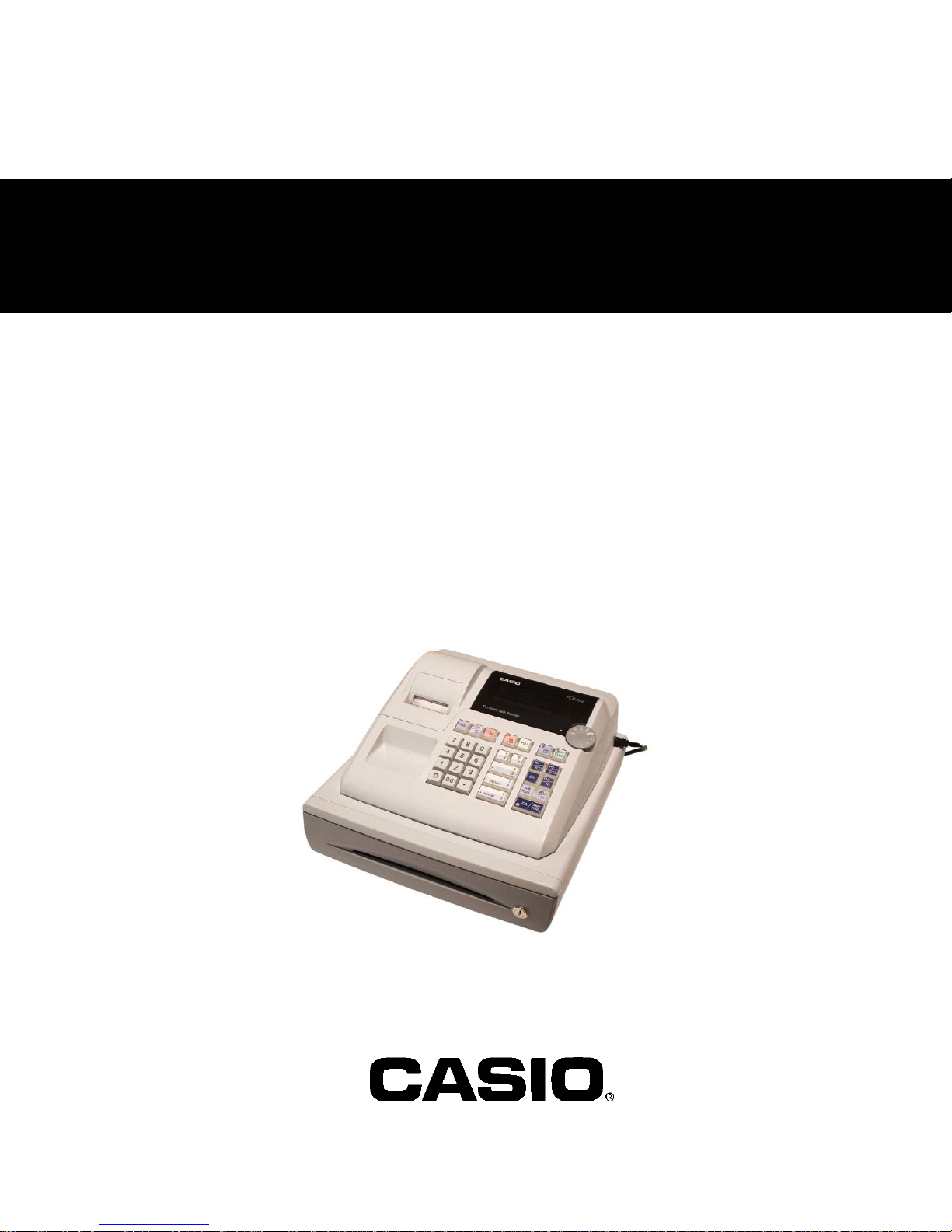
ELECTRONIC CASH REGISTER
130CR/PCR-262/CE-160
(EX-264)
JAN. 2005
Page 2

CONTENTS
130CR/PCR-262/CE-160 Page
1. SPECIFICATIONS........................................................................................ 1
2. MACHINE INTIALIZATION .......................................................................... 3
3. BLOCK DIAGRAM....................................................................................... 4
4. DISASSEMBLY............................................................................................ 5
5. CIRCUIT EXPLANATION ............................................................................ 9
6. DIAGNOSTIC OPERATIONS .................................................................... 16
7. TROUBLESHOOTING ............................................................................... 20
8. IC DATA ..................................................................................................... 21
9. PCB LAYPUT............................................................................................. 22
10. CIRCUIT DIAGRAM ................................................................................... 23
11. PARTS LIST............................................................................................... 27
Page 3
1. SPECIFICATIONS
1-1. Electrical specifications
• Power consumption In operation Max. 0.1 A 0.05 A 0.05 A 0.05 A
• Memory protection Back-up battery Mangan Battery (UM-3 × 3 pcs)
Back-up period 1 year (25 °C)
Battery life Replace the battery every 1 years.
• Clock & Calendar Accuracy Within ± 30 sec. per month
Auto calendar Effective until 2099 A.D.
1-2. Environmental specifications
• Operating temperature 0 °C ~ 40 °C
• Operating humidity 10 % ~ 90 %
• Storage temperature -25 °C ~ 65 °C
• Storage humidity 10 % ~ 95 %
120 V 220 V 230 V 240 V
• Vibration strength 1.5 G (The machine must be in the carton box)
1-3. Main components
• CPU Name UPD780058BGC124-8BTA
Number of control bit 8 bit
Mask ROM (Built-in) 60 Kbytes
RAM (Built-in) 1024 bytes
• Printer Name M-42V-009-040
Print method Print wheel selecting type serial printer
MCBF 700,000 lines
• Roll paper Type Fine-quality paper
Size Width 57.5 ± 0.5 mm
Roll diameter 80 mm or less
1-4. Drawer List
DRAWER NAME Specification NOTE
• DL-1329A (S type) D-21G2M-D54RM-16A U.S.A
• DL-1841A (S type) D-21G2M-D53RM-16A UK/Germany, Europe, Other countries
• DL-2794A (M type) D-18G2C-B84RM-13A Europe, Other countries
• DL-2796A (M type) D-18G2C-A84RM-13A Canada
— 1 —
Page 4

1-5. Option List
DEVICE NAME MODEL NOTE
• Wet cover WT-80
• Roll paper P-5860 58 x 12 x 60D
CAUTION
Danger of explosion if battery is incorrectly replaced.
Replace only with the same or equivalent type
recommended by the manufacturer.
Dispose of used batteries according
to the manufacture’s instructions.
VORSICHT !
Explosionsgefahr bei unsachgemäßem Austausch der Batterie.
Ersatz nur durch denselben oder einen vom
Hersteller empfohlenen gleichwertigen Typ.
Entsorgung gebrauchter Batterien nach
Angaben des Herstellers.
ADVARSEL !
Lithiumbatteri - Eksplosionsfare ved fejlagtig hándtering.
Udskiftning má kun ske med batteri
af samme fabrikat og type.
Levér det brugte batteri tilbage til leverandØren.
— 2 —
Page 5
2. MACHINE INTIALIZATION
2-1. Initialization and loading memory protection battery
Note: You must initialize the cash register and install the memory protection batteries before you can
program the cash register.
To initialize the cash register
1. Set the mode switch to OFF.
2. Plug the power cord of the cash register into an AC outlet.
3. Load the memory protection batteries.
4. Set the mode switch to REG.
To load the memory protection batteries
1. Remove the printer cover.
2. Open the battery compartment cover.
3. Load 3 new UM-3, R6P (SUM-3) or LR6 (AM-3) type batteries into the compartment.
Be sure that the plus (+) and minus (–) ends of each battery are facing in the directions indicated by
the illustrations inside the battery compartment.
4. Slide the memory protection battery compartment cover back into place.
5. Replace the printer paper and printer cover.
REPLACE MEMORY PROTECTION BATTERIES AT LEAST ONCE EVERY YEAR.
2-2. To select the date format and monetary mode (130CR only)
You can select the date format and the monetary mode after initialization depending on the requirements in your
area.
Default date format is Day/Month/Year.
Default Monetary Mode is Add 2.
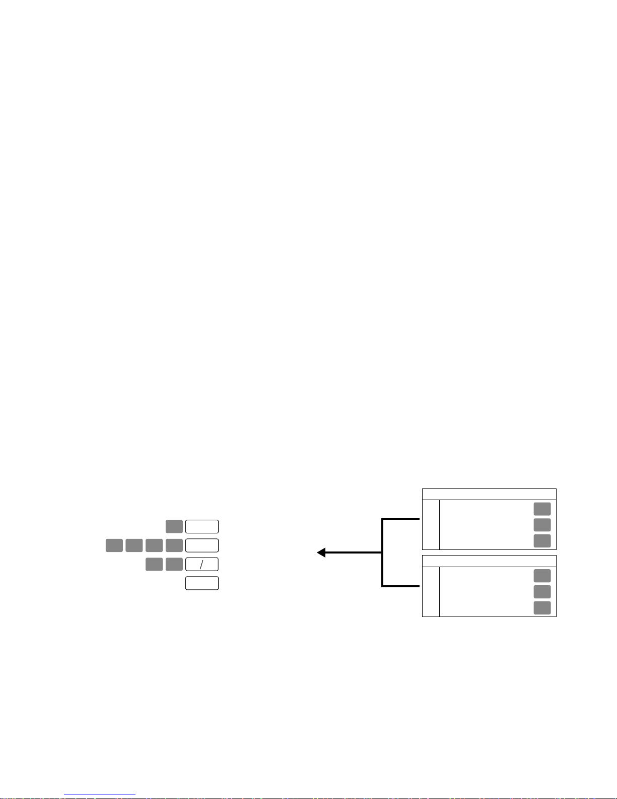
Example: Change the date format to Month/Day/Year, and the monetary mode to Add 0.
1. Set the mode switch to PGM.
2. Press the following keys.
Date format selections
0 1 2 2
1 0
3
SUB
TOTAL
SUB
TOTAL
CA AMT
= TEND
SUB
TOTAL
P3 appears in mode display
Program set code number
Select numbers from
lists A and B.
(To end the setting)
Year/Month/Day
Month/Day/Year
A
Day/Month/Year
Monetary mode selections
Add 0 (0. )
Add 1 (0.0 )
B
Add 2 (0.00 )
0
1
2
0
1
2
— 3 —
Page 6
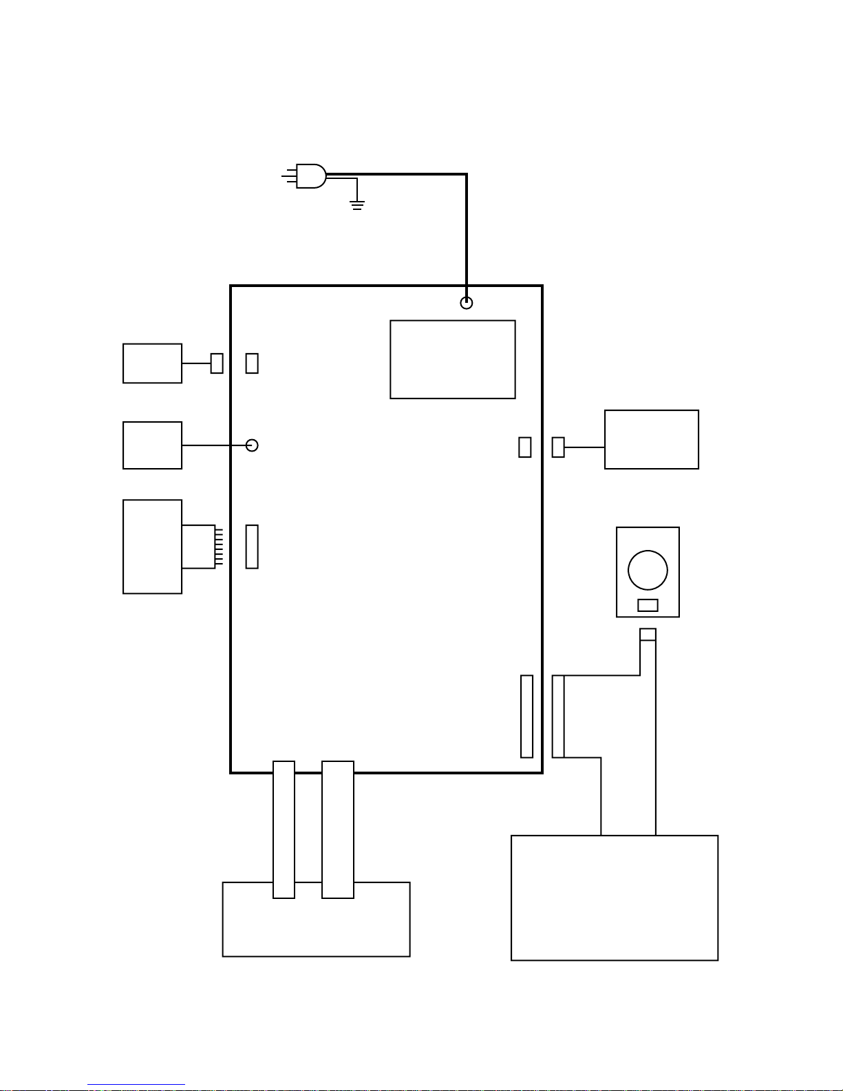
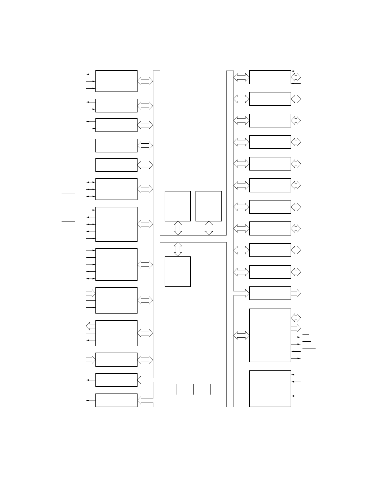
3. BLOCK DIAGRAM
2P
DRAWER
WINDER
MOTOR
PRINTER
M-42V
2P
2P
8P
TRANSFORMER
TE-264-***
E-264-1
21P
2P
BATTERY
UM-3(PZ) X3
MODE SWITCH
8P
8P 12P
PARALLEL CABLE
DISPLAY
PARALLEL CABLE
KEY BOARD
— 4 —
Page 7
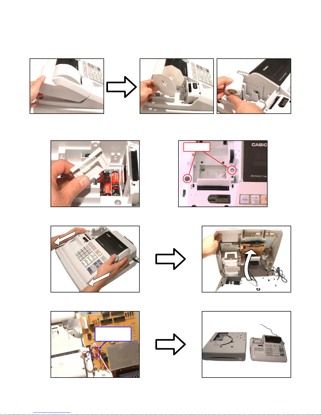
4. DISASSEMBLY
■ Removing the register
1. Remove the journal cover and then the WINDING PULLY and ROLL PAPER.
2. Remove the battery cover and then the battery.
3. Remove the two screws.
Screws
4. Separate the main unit as shown below.
5. Remove the connector (CNDRW1) and then separate the main unit from the drawer.
Connector
(CNDRW1)
— 5 —
Page 8
■ Removing the Main PCB and Display PCB
6. Remove the three connectors (CNKEY1, CNBAT1, CNPR1) and the four screws.
7. Remove the two hooks and then Main PCB.
Connector
(CNKEY1)
Hook
Screws
8. Remove the two hooks and then Display PCB.
Hooks
Hook
Connector
(CNBAT1)
Connector
(CNPR1)
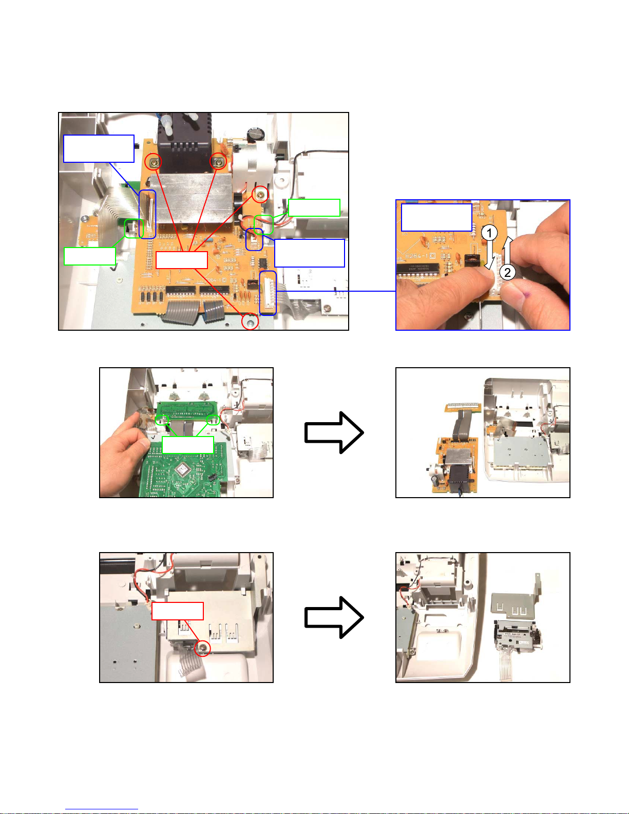
■ Removing the printer unit
9. Remove one screw and then the printer unit.
Screw
— 6 —
Page 9
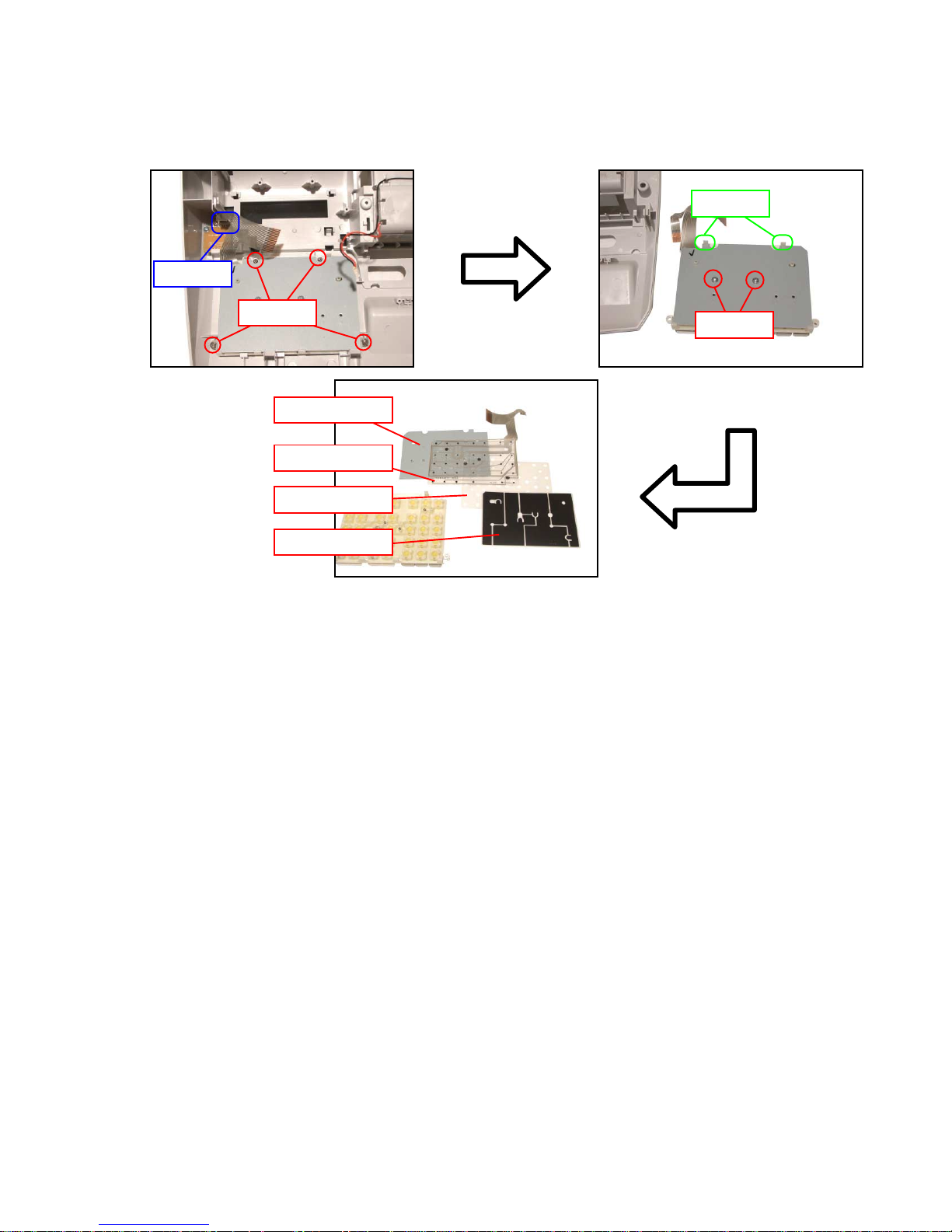
■ Disassembling the keyboard unit
10.Remove the FPC as well as the four screws, and then the keyboard unit.
11. Remove the two screws and then disassemble the keyboard unit.
FPC
Hooks
Screws
Chassis
Common sheet
Spacer
Screws
FPC
— 7 —
Page 10
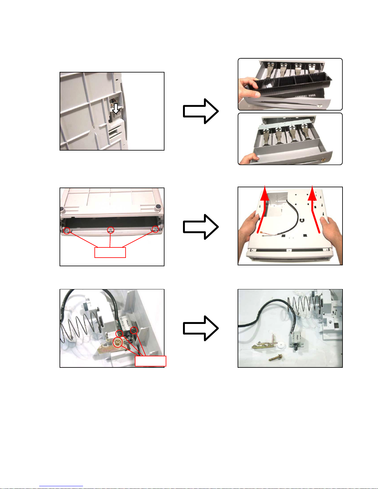
■ Disassembling the drawer
1. Pull the lever and remove the coin case and bill case.
2. Remove the three screws and then the top plate.
Screws
3. Remove the three screws and the solenoid.
Screws
— 8 —
Page 11

5. CIRCUIT EXPLANATION
5-1. CPU (IC3: uPD780058BGC124-8BTA)
5-1-1. Pin Assignment
P14/ ANI4
P13/ ANI3
P12/ ANI2
P11/ ANI1
P10/ ANI0
REF0
AV
DD0
V
XT1/ P07
)
PP
XT230IC (V
X1
X2
DD1
V
SS0
V
P05/ INTP5
P04/ INTP4
P03/ INTP3
P02/ INTP2
P01/ INTP1/ TI01
P00/ INTP0/ TI00
P15/ANI5 1
P16/ANI6
P17/ANI7
AV
P130/ANO0
P131/ANO1
REF1
AV
P70/SI2/RxD0
P71/SO2/TxD0
P72/SCK2/ASCK
P20/SI1
P21/SO1
P22/SCK1
P23/STB/TxD1
P24/BUSY/RxD1
P25/SI0/SB0
P26/SO0/SB1
P27/SCK0
P40/AD0
P41/AD1
80 79 78 77 76 75 74 73 72 71 70 69 68 67 66 65 64 63 62
2
3
SS
4
5
6
7
8
9
10 51
11 50
12 49
13 48
14 47
15 46
16 45
17 44
18 43
19 42
20 41
21
22
23
24
25
26
27
28
29
31
32
33
34
35
36
37
P42/ AD2
P43/ AD3
P44/ AD4
P45/ AD5
P46/ AD6
P47/ AD7
P50/ A8
P51/ A9
P52/ A10
P53/ A11
P54/ A12
P55/ A13
SS1
V
P60
P56/ A14
P57/ A15
38
P61
39
P62
61
60
59
58
57
56
55
54
53
52
40
P63
P64/ RD
RESET
P127/RTP7
P126/RTP6
P125/RTP5
P124/RTP4
P123/RTP3
P122/RTP2
P121/RTP1
P120/RTP0
P37
P36/BUZ
P35/PCL
P34/TI2
P33/TI1
P32/TO2
P31/TO1
P30/TO0
P67/ASTB
P66/WAIT
P65/WR
— 9 —
Page 12
5-1-2. Block Diagram
TO0/P30
TI00/P00
TI01/P01
TO1/P31
TI1/P33
TO2/P32
TI2/P34
SI0/SB0/P25
SO0/SB1/P26
SCK0/P27
SI1/P20
SO1/P21
SCK1/P22
STB/TxD1/P23
BUSY/RxD1/P24
BUSY/RxD1/P24
STB/TxD1/P23
SI2/RxD0/P70
SO2/TxD0/P71
SCK2/ASCK/P72
16-bit timer/
event counter
8-bit timer/
event counter 1
8-bit timer/
event counter 2
Watchdog timer
Watch timer
Serial interface 0
Serial interface 1
Serial interface 2
78K/0
CPU core
RAM
ROM
(flash
memory)
Port 0
Port 1
Port 2
Port 3
Port 4
Port 5
Port 6
Port 7
Port 12
Port 13
P00
P01 to P05
P07
P10 to P17
P20 to P27
P30 to P37
P40 to P47
P50 to P57
P60 to P67
P70 to P72
P120 to P127
P130, P131
ANI0/P10 to
ANI7/P17
AV
AVREF0
ANO0/P130,
ANO1/P131
AV
AVREF1
INTP0/P00 to
INTP5/P05
BUZ/P36
PCL/P35
SS
SS
A/D converter
D/A converter
Interrupt control
Buzzer output
Clock output control
V
V
DD0,
DD1
V
V
SS0,
SS1
(V
IC
PP)
Real-time output port
External access
RTP0/P120 to
RTP7/P127
AD0/P40 to
AD7/P47
A8/P50 to
A15/P57
RD/P64
WR/P65
WAIT/P66
ASTB/P67
RESET
X1
X2System control
XT1/P07
XT2
— 10 —
Page 13
5-1-3. Pin Function
(1) Port pins (1/2)
Pin Name
P00
P01
P02
P03
P04
P05
Note 1
P07
P10 to P17
P20
P21
P22
P23
P24
P25
P26
P27
P30
P31
P32
P33
P34
P35
P36
P37
I/O
Input
I/O
Port 0
7-bit I/O port
Function
Input only
Input/output can be specified in 1-bit
units.
If used as an input port, an on-chip
pull-up resistor can be connected by
setting software.
Input
I/O
Port 1
Input only
8-bit I/O port
Input/output can be specified in 1-bit units.
If used as an input port, an on-chip pull-up resistor can
be connected by setting software.
I/O
Port 2
Note 2
8-bit I/O port
Input/output can be specified in 1-bit units.
If used as an input port, an on-chip pull-up resistor can
be connected by setting software.
I/O
Port 3
8-bit I/O port
Input/output can be specified in 1-it units.
If used as an input port, an on-chip pull-up resistor can
be connected by setting software.
After Reset
Input
Input
Input
Input
Input
Input
Alternate Function
INTP0/TI00
INTP1/TI01
INTP2
INTP3
INTP4
INTP5
XT1
ANI0 to ANI7
SI1
SO1
SCK1
STB/TxD1
BUSY/RxD1
SI0/SB0
SO0/SB1
SCK0
TO0
TO1
TO2
TI1
TI2
PCL
BUZ
—
Notes
1. When the P07/XT1 pin is used as an input port, set bit 6 (FRC) of the processor clock control register
(PCC) to 1 (do not use the feedback resistor incorporated in the subsystem clock oscillator).
2. When pins P10/ANI0 to P17/ANI7 are used as an analog input of the A/D converter, set port 1 to the
input mode. In this case, any connected on-chip pull-up resistors are automatically disabled.
— 11 —
Page 14
(1) Port pins (2/2)
Pin Name
P40 to P47
P50 to P57
P60
P61
P62
P63
P64
P65
P66
P67
P70
P71
P72
I/O
I/O
Port 4
Function
8-bit I/O port
Input/output can be specified in 8-bit units.
If used as an input port, an on-chip pull-up resistor can
be connected by setting software.
The test input flag (KRIF) is set to 1 by falling edge
detection.
I/O
Port 5
8-bit I/O port
LEDs can be driven directly.
Input/output can be specified in 1-bit units.
If used as an input port, an on-chip pull-up resistor can
be connected by setting software.
I/O
Port 6
8-bit I/O port
Input/output can be
specified in 1-bit units.
N-ch open-drain I/O port
On-chip pull-up resistors can
be specified by mask option.
(Mask ROM version only).
LEDs can be driven directly.
If used as an input port, an onchip pull-up resistor can be
connected by setting software.
I/O
Port 7
3-bit I/O port
Input/output can be specified in 1-bit units.
If used as an input port, an on-chip pull-up resistor can
be connected by setting software.
After Reset
Input
Input
Input
Input
Alternate Function
AD0 to AD7
A8 to A15
—
RD
WR
WAIT
ASTB
SI2/RxD0
SO2/TxD0
SCK2/ASCK
P120 to P127
P130 to P131
I/O
Port 12
8-bit I/O port
Input/output can be specified in 1-bit units.
If used as an input port, an on-chip pull-up resistor can
be connected by setting software.
I/O
Port 13
2-bit I/O port
Input/output can be specified in 1-bit units.
If used as an input port, an on-chip pull-up resistor can
be connected by setting software.
— 12 —
Input
Input
RTP0 to RTP7
ANO0 to ANO1
Page 15

(2) Non-port pins (1/2)
Pin Name
INTP0
INTP1
INTP2
INTP3
INTP4
INTP5
SI0
SI1
SI2
SO0
SO1
SO2
SB0
SB1
SCK0
SCK1
SCK2
STB
BUSY
RxD0
RxD1
TxD0
TxD1
ASCK
TI00
TI01
TI1
TI2
TO0
TO1
TO2
PCL
BUZ
RTP0 to RTP7
I/O
I/O
I/O
Output
I/O
I/O
Output
Input
Input
Output
Input
Input
Output
Output
Output
Outpu
Function
External interrupt request inputs with specifiable
valid edges (rising edge, falling edge, both rising and
falling edges).
Serial interface serial data input
Serial interface serial data output
Serial interface serial data input/output
Serial interface serial clock input/output
Serial interface automatic transmit/receive strobe
output
Serial interface automatic transmit/receive busy input
Asynchronous serial interface serial data input
Asynchronous serial interface serial data output
Asynchronous serial interface serial clock input
External count clock input to 16-bit timer (TM0)
Capture trigger signal input to capture register (CR00)
External count clock input to 8-bit timer (TM1)
External count clock input to 8-bit timer (TM2)
16-bit timer (TM0) output (also used for 14-bit PWM
output)
8-bit timer (TM1) output
8-bit timer (TM2) output
Clock output (for main system clock and subsystem
clock trimming)
Buzzer output
Real-time output port outputting data in
synchronization with trigger
After Reset
Input
Input
Input
Input
Input
Input
Input
Input
Input
Input
Input
Input
Input
Input
Alternate Function
P00/TI00
P01/TI01
P02
P03
P04
P05
P25/SB0
P20
P70/RxD
P26/SB1
P21
P71/TxD
P25/SI0
P26/SO0
P27
P22
P72/ASCK
P23/TxD1
P24/RxD1
P70/SI2
P24/BUSY
P71/SO2
P23/STB
P72/SCK2
P00/INTP0
P01/INTP1
P33
P34
P30
P31
P32
P35
P36
P120 to P127
— 13 —
Page 16

(2) Non-port pins (2/2)
Pin Name
AD0 to AD7
A8 to A15
RD
WR
WAIT
ASTB
ANI0 to ANI7
ANO0, ANO1
AVREF0
AVREF1
AVSS
RESET
X1
X2
XT1
XT2
VDD0
VSS0
VDD1
VSS1
VPP
IC
I/O
I/O
Output
Output
Input
Output
Input
Output
Input
Input
—
Input
Input
—
Input
—
—
—
—
—
—
—
Function
Lower address/data bus when expanding memory
externally
Higher address bus when expanding memory
externally
Strobe signal output for read operation from external
memory
Strobe signal output for write operation to external
memory
Wait insertion when accessing external memory
Strobe output externally latching address information
output to ports 4 and 5 to access external memory
A/D converter analog input
D/A converter analog output
A/D converter reference voltage input (also functions
as analog power supply)
D/A converter reference voltage input
A/D converter, D/A converter ground potential. Use
the same potential as VSS0.
System reset input
Crystal connection for main system clock oscillation
Crystal connection for subsystem clock oscillation
Positive power supply for ports
Ground potential for ports
Positive power supply (except ports and analog
block)
Ground potential (except ports and analog block)
High-voltage application for program write/verify.
Internally connected. Connect directly to VSS0.
After Reset
Input
Input
Input
Input
Input
Input
Input
—
—
—
—
—
—
Input
—
—
—
—
—
—
—
Alternate Function
P40 to P47
P50 to P57
P64
P65
P66
P67
P10 to P17
P130, P131
—
—
—
—
—
—
P07
—
—
—
—
—
—
—
— 14 —
Page 17

5-2. Reset circuit/Printer circuit/Power circuit
Reset circuit
100u/10V
Printer circuit
VP
C6
CNWIN1
PN1
PN2
2P-SAN
CNPR1
MAG-
MAG+
MOT+
MOT-
TIM
RES
COM
TS
52011-0810
1
2
8
7
6
ECQ-B1H103-KF
5
4
3
2
1
C26
HE40TKYB221K
R60 ERG-1SJ100
CM05RB03
L1
1 3
2 4
R74 1K
R75 1K
DSTC50TKYR103K
DSTC50TKYR103K
R76 1K
VP
C24
C25
HE60TKYB222K
VDD
TRES
R26
VDD
IC2
2
Vout
C7
Vin
S-80828CNY
C28
Vss
VP
C30 330u/10V
100K
100K
R72
C27
HE60TKYB222K
R73
1
3
IC4
8
7
6
5
C29
OUT1
IN1
IN2
OUT2
IN3
OUT3
GND
VCC
LB1268
100K
R71
HE60TKYB222K
100K
C8 ECQ-B1H103-KF
1
2
3
4
IC3:uPD780058BGC124-8BTA
60
/RESET
11
P20
13
P22
12
P21
16
P25
61
P00
64
P03
63
P02
Power circuit
AC IN
N
5298T
AC IN
N100V
5298T
CNAC1
1
S1
2
S2
3
S3
4
S4
5
S5
6
S6
7
S7
7P-SDN
AC IN
L
5298T
T1
NC
1
2
3
4
5
TE-264-E1U/TE-264-E1D
NC
10
F1
1 2
9
630/800mA
(8)
7
TE12TKYB103K
6
VDW
TDW
TVP
TLED
TVD
VDD
VLED
VDD
VP
62
P01(INTP1)
Q1
2SD2396
32
ZD2
MTZJ4.7A
1
ERG-12SJ681P
D4
C1
1SR139-400
1SR139-400
1SR139-400
D3
1SR139-400
4700u/25V
R1
D2
D1
C2
ZD1
MTZJ6.8A
330u/25V
C4
R14 150
1
R13
560
IC1
BA05CC0T
IN
OUT
G
2
3
2SC1740S
C3
3
Q2
1 2
RB441Q-40
R11 470K
C5
ECQ-B1H103-KF
D5
100u/10V
— 15 —
Page 18

6. DIAGNOSTIC OPERATION
To start the diagnostic program
ECR enters the diagnostic mode by the following operation.
1 Turn the mode key to PGM.
2 Input “99990000” and “ST(SUB TOTAL)”.
Upon the above operation ECR prints the following and issues a receipt.
* Note that the test mode will not boot if once a receipt has been issued in the REG/RF/X/Z mode.
In this case, remove the battery and perform the above operation again.
2000-00-00
00-00#0001
-d1d2d3d4--d5d6d7
d1d2d3d4: Version No.
d5: Destination PAD
0: domestic
1: general export (ADD2)
2: US/Canada
d6: 0: tax spec
1: no tax spec
“-”: overseas
07: 0: domestic
“-”: overseas
* “#” is not printed for US and Canada.
6-1. Content of the Test
1 Displaying the Key Code ......................... Press any key other than the ten keys and clear key.
2 Displaying the Switch Condition .............. Press the clear key, or change the status of switches.
3 Printing, Display and Drawer test ............ One digit number + “ST(SUB TOTAL)” key
6-2. Displaying the Key Code
Press any key other than the ten keys and clear key to dipslay the hard key code as shown below.
(Display) 019
FEED
029 C
7 8 9
4 5 6
1 2 3
0 011 012
028 023
027 022
026
025
024
021 017
020 016
019 015
018 014
013 013
— 16 —
Page 19

6-3. Displaying the Switch Condition
Press the clear key, or change the status of switches to display the current conditions.
[DISPLAY]
Mode SW
1:PGM, 2:RF, 4:REG,
5:CAL, 6:X, 7:Z, 0:no contact
FEED key
1:ON, 0:OFF
No tax PAD (film)
1: tax (default)
0: no tax (cut)
PAD2
1:SHORT
0:OPEN
PAD1
1:SHORT
0:OPEN
No display
No display
0:Fixed
— 17 —
Page 20

6-4. Operations
■ Bulk test
Operation : 1 ST (SUB TOTAL)
All lit in the display, time and date setting, drawer open.
• All lit
(display) : 88888888=
↑ (transaction)
• Waits for key input
• Time and date setting
Set the time and date at 23:59 on 31 December, 1994.
• Drawer open
• Test print
US: 123456789012ST#
Other than US: 1234567890ST#
•Test display
(display) : 12345678
■ Switching the Receipt / Journal
Operation : 2 ST (SUB TOTAL)
This test switches the printing between the receipt and the journal.
■ Battery test
Operation : 7 ST (SUB TOTAL)
This test displays the battery voltage value.
The battery voltage is displayed until a power down occurs.
(display) : BBB BBB: battery voltage
Ex) when the voltage is 2.56V, “BBS=256” is displayed.
— 18 —
Page 21

■ Battery test
Operation : 8 ST (SUB TOTAL)
All the fonts are printed.
US (Total of 14 digits) Other than US (Total of 12 digits)
Blank line
■ Time display test
Operation : 9 ST (SUB TOTAL)
Time is displayed until the clear key is pressed or a power down occurs.
■ Ending the test mode
To leave the test mode, remove the battery (AUTO MAC).
— 19 —
Page 22

7. TROUBLESHOOTING
130CR
Symptom/Problem
1
E01 appears on the display.
2
E94 appears on the display.
3
No date or time on receipt.
Paper is not advancing enough.
4
Drawer opens up after ringing
up only one time.
5
Not clearing totals at end of day
after taking report.
6
Programming is lost whenever
register is unplugged or there is
a power outage.
7
Register is inoperative.
Can’t get money out of drawer.
Most common causes
Changing modes without
completing transaction.
Printer paper is jammed.
Printer is programmed as a
journal.
Department is programmed as
a single item dept.
Using X mode to take out reports.
Bad or no batteries.
No power.
Solutions
Return mode switch to
where it stops buzzing and
CA AMT
press
= TEND
.
Remove jammed paper.
Turn Mode switch to OFF
then turn to ON, or Turn
power OFF and then turn
power ON.
Program printer to print
receipts.
Program the dept. as a
normal dept.
Use Z mode to take out
reports.
Put in new batteries.
Pull lever underneath
register at rear.
PCR262/CE160
1
E01 appears on the display.
2
E08 appears on the display.
3
E94 appears on the display.
4
No date or time on receipt.
Paper is not advancing enough.
5
Drawer opens up after ringing
up only one time.
6
Not clearing totals at end of day
after taking report.
7
Programming is lost whenever
register is unplugged or there is
a power outage.
Symptom/Problem
Most common causes
Changing modes without
completing transaction.
Sign on operation is not
perfomed.
Printer paper is jammed.
Printer is programmed as a
journal.
Department is programmed as
a single item dept.
Using X mode to take out reports.
Bad or no batteries.
Solutions
Return mode switch to
where it stops buzzing and
CA AMT
press
= TEND
.
Prior to starting registration
of any other operation,
press “1” ~ “8” and then
CA AMT
= TEND
.
Remove jammed paper. Turn
Mode switch to OFF then turn
to ON, or Turn power OFF
and then turn power ON.
Program printer to print
receipts.
Program the dept. as a
normal dept.
Use Z mode to take out
reports.
Put in new batteries.
8
Register is inoperative.
Can’t get money out of drawer.
No power.
— 20 —
Pull lever underneath
register at rear.
Page 23

8. IC DATA
1. BA05CC0T (IC1)
Pin No.
1
2
3
2. S-80828CNY (IC2)
Pin name
Vcc
GND
OUT
1
2
3
Description
Input Power Supply
GND
Output Power Supply
OUT
V
DD
V
SS
Vcc
Vref
Driver
R2
R1
OCP
TSDOVP
21
GND
2
V
DD
+
3
OUTVcc
OUT
1
*
VEFR
Bottom view
312
3. LB1268 (IC4)
TOP VIEW
1
IN1
2
IN2
3
IN3
4
GND
4. TD62083AP (IC5, 6)
3
V
SS
* Parasitic diode
15K
TR5
OUT3
VCC
120
1K
D3
TR6
GND
8
7
6
5
OUT1
OUT2
OUT3
VCC
OUT1
240
TR1
6.8K
IN1 IN2
TR2
6.8K
OUT2
D1
240
TR3
30K30K
2K2K
D2
3.4K
TR4
IN3
PIN DESCRIPTIONS
PIN 1~3: IN1~IN3 - Contr o l s ignal input pin.
PIN 4: GND - Power ground.
PIN 5: VCC - The output pin (Cathode) of freewheeling diode.
PIN 6~8: OUT1~3 - Each of the pi ns m ay i ndi vidually sink load current from some controlled circuits.
O4O1 O5 O6 O7 O8 COMMONO3O2
1518 14 13 12 11 101617
41 5678932
I4I1 I5 I6 I7 I8 GNDI3I2
— 21 —
Page 24

9. PCB LAYPUT
— 22 —
Page 25

10. CIRCUIT DIAGRAM
MODEL : 130CR/PCR-262/CE-160
(EX-264)
CONTENTS
1. MAIN BOARD ........................................................................................................................... 24
2. DISPLAY BOARD.................................................................................................................... 25
3. MODE KEY.............................................................................................................................. 26
— 23 —
Page 26

— 24 —
Model
NameBoard No.
Drawing No.
CASIO COMPUTER CO.,LTD.
R23
56K
Q8
2SB1237
R46
100
R64 510
IC1
BA05CC0T
C28
HE60TKYB222K
IC3
uPD780053GC /
uPD780058BGC
R22
56K
R41 100
CAB2
6820SUS
Q4
DTA143ZSA
Q2
2SC1740S
C1
TE12TKYB103K
R66 510
R52
1.5M
CNSW1
52045-0445
R7
10K
C30 330u/10V
C13 100p
R55 56K
R18 56K
ZD1
MTZJ6.8A
R53 56K
R60 ERG-1SJ100
R73
100K
R59 56K
R69 56K
R49 56K
D5
RB441Q-40
R16 56K
C21
HE40TKYB221K
R62 510
R25
100
R68 510
D9 1SS133
C24
DSTC50TKYR103K
D6
1SS133
R30
56K
R21
56K
C8 ECQ-B1H103-KF
R26
100K
R43 100
Q7
2SB1237
R4
56K
5298T
Q5
2SD1853
R74 1K
D3
1SR139-400
TDW
C18
DSTC50TKYR103K
R33
56K
R63 1K
C20
15p
C5
ECQ-B1H103-KF
PAD1
R35 100
R13
560
R20 1K
CNWIN1
2P-SAN
TVP
R37 100
CNBAT1
5267-02A-X
R72
100K
R45 100
C2
4700u/25V
C25
DSTC50TKYR103K
R6
10K
ZD2
MTZJ4.7A
X1
CST5.00MGW
R31
56K
R56 56K
Q6
2SB1237
R51
ERX-1SJ1R2P
R76 1K
TRES
C9
HE60TKYB222K
R27
56K
C4
330u/25V
R10
10KR556K
C27
HE60TKYB222K
D8
1SS133
R2
10K
R50
330K
C7
100u/10V
CAB1
61320SUS
Q3
DTC114YSA
R38
100
R47 100
PAD2
D1
1SR139-400
F1
630/800mA
L1
CM05RB03
C15 100p
CNDRW1
IL-G-2P-S3T2-SA
C29
HE60TKYB222K
BZ1
PKM22EPT-2001-B0
C11 100p
R61 1K
R9
56K
Q1
2SD2396
R34
100
TVD
R42
100
R57 56K
R70 56K
R32
56K
CNPR1
52011-0810
R75 1K
R65 1K
Q9
2SB1237
R28
56K
D11
1SR139-400
R24
56K
C17 100p
R67 1K
IC5
TD62083AP
R17 56K
R3
10K
5298T
C3
100u/10V
R11 470K
R39 100
Q10
DTC114YSA
R54 56K
CNKEY1
52045-2145
R15 56K
T1
TE-264-E1U/TE-264-E1D
NC
NC
D10 RB721Q-40
R44
100
C6
HE40TKYB221K
IC2
S-80828CNY
C22
DSTC50TKYR103K
CNAC1
7P-SDN
D7 1SS133
5298T
C14 100p
C10 100p
C16 100p
C12 100p
R14 150
R8
56K
IC4
LB1268
C23
DSTC50TKYR103K
R58 56K
R71
100K
R48 56K
D2
1SR139-400
R19 1K
C19
15p
TLED
D4
1SR139-400
X2
C-002RX-8.3/10
R12 10K
C26
ECQ-B1H103-KF
R40
100
R29
56K
R1ERG-12SJ681P
IC6
TD62083AP
R36
100
VDD
VDD VDD
VDD
VLED
VP
VLED
VDD
VLED
VDD
VP
VDW
VDD
VP
VP
VP
VDD
VDD
VDW
VDD
VDD
VDD
VLED
3
12
IN
1
OUT
3
G
2
P36(BUZ)
50
P02
63
P01(INTP1)
62
P00
61
P70
8
P71
9
P72
10
P03
64
/RESET
60
X1
70
X2
69
XT2
72
XT1
73
AVref1
7
AVref0
75
AVss
4
VDD1
68
Vss0
67
IC
71
VDD0
74
Vss1
33
P60
36
P61
37
P62
38
P63
39
P120
52
P121
53
P122
54
P123
55
P124
56
P125
57
P126
58
P127
59
P64
40
P65
41
P66
42
P67
43
P20
11
P21
12
P22
13
P23
14
P30
44
P31
45
P32
46
P33
47
P34
48
P35
49
P04
65
P40
19
P41
20
P42
21
P43
22
P44
23
P45
24
P46
25
P47
26
P50
27
P51
28
P52
29
P53
30
P54
31
P55
32
P56
34
P57
35
P05
66
P12
78
P13
79
P15
1
P16
2
P17
3
P24
15
P25
16
P26
17
P27
18
P37
51
P130
5
P131
6
P10(ANI0)
76
P11
77
P14
80
1
2
3
4
5
6
7
8
3
12
3
1 2
S1
1
S2
2
S3
3
S4
4
3
12
3
1 2
PN1
1
PN2
2
BAT+
2
BAT-
1
1
3
2
3
12
1
2
3
4
5
6
7
8
9
10
11
12
13
3
21
1 2
1 3
2 4
VC
2
CO
1
1 2
1
32
MAG-
8
MAG+
7
MOT+
6
MOT-
5
TIM
4
RES
3
COM
2
TS
1
3
12
I1
1
I2
2
I3
3
I4
4
I5
5
I6
6
I7
7
O1
18
O2
17
O3
16
O4
15
O5
14
O6
13
O7
12
COM
10
GND
9
I8
8O811
3
21
KI2a
1
KI1
2
KI7
3
KI6
4
KC3
5
KI5
6
KI4
7
KC2
8
KC1
9
KI3
10
KI2b
11
KI0
12
KC0
13
COM
14
Z
15
X
16
CAL
17
REG
18
OFF
19
RF
20
PGM
21
6
1
2
4
5
3
7
9
10
(8)
Vout
1
Vin
2
Vss
3
S1
1
S2
2
S3
3
S4
4
S5
5
S6
6
S7
7
IN1
1
IN2
2
IN3
3
GND
4
VCC
5
OUT3
6
OUT2
7
OUT1
8
1
2
I1
1
I2
2
I3
3
I4
4
I5
5
I6
6
I7
7
O1
18
O2
17
O3
16
O4
15
O5
14
O6
13
O7
12
COM
10
GND
9
I88O8
11
AC IN
AC IN
AC IN
N100V
N
L
No Mount
EX-264 E264-1 A MAIN BOARD RJE501400D203
Page 27

61320SUS
CAB4
CAB3
12345678910111213
1234567
6820SUS
8
R109 150
R117 150
R110 150
R113 150
R112 150
R101 150
R116 150
R111 150
R108 150
R103 150
R105 150
R106 150
R107 150
R104 150
R102 150
R114 150
R115 150
DSP1
HDSP-521G
1
2
3
4
5
6
7
8
9
e1
d1
c1
DP1
e2
d2
g2
c2
DP2
18
f1
17
g1
16
a1
15
b1
14
DI1
13
DI2
12
f2
11
a2
10
b2
DSP2
HDSP-521G
1
2
3
4
5
6
7
8
9
e1
d1
c1
DP1
e2
d2
g2
c2
DP2
18
f1
17
g1
16
a1
15
b1
14
DI1
13
DI2
12
f2
11
a2
10
b2
D102 HLMP-S501
D101 HLMP-S501
DSP3
HDSP-521G
1
2
3
4
5
6
7
8
9
e1
d1
c1
DP1
e2
d2
g2
c2
DP2
18
f1
17
g1
16
a1
15
b1
14
DI1
13
DI2
12
f2
11
a2
10
b2
Model
CASIO COMPUTER CO.,LTD.
DSP4
HDSP-521G
1
2
3
4
5
6
7
8
9
e1
d1
c1
DP1
e2
d2
g2
c2
DP2
18
f1
17
g1
16
a1
15
b1
14
DI1
13
DI2
12
f2
11
a2
10
b2
NameBoard No.
Drawing No.
EX-264 E264-E2 A DISPLAY BOARD RJE501400D304
— 25 —
Page 28

SW1
COM
MODE_KEY
CN1
1
PGM
2
RF
3
OFF
4
REG
5
CAL
6
X
7
Z
8
52045-0845
Model
CASIO COMPUTER CO.,LTD.
NameBoard No.
Drawing No.
EX-264 E264-E3 C MODE KEY RJE501400D405
— 26 —
Page 29

11. PARTS LIST
MODEL : 130CR/PCR-262/CE-160
(EX-264)
Explode view...........................................................................................................................................28
130CR
1. MAIN PCB BLOCK & MAIN DISPLAY BLOCK ............................................................................... 30
2. BUTTON BLOCK ............................................................................................................................. 31
3. POWER CORD BLOCK .................................................................................................................. 32
4. UPPER CASE BLOCK .................................................................................................................... 32
PCR262&CE160
1. MAIN PCB BLOCK & MAIN DISPLAY BLOCK ............................................................................... 33
2. BUTTON BLOCK ............................................................................................................................. 34
3. POWER CORD BLOCK .................................................................................................................. 35
4. UPPER CASE BLOCK .................................................................................................................... 35
5. DRAWER (DL-1329A) ..................................................................................................................... 36
6. DRAWER (DL-1841A) ..................................................................................................................... 38
7. DRAWER (DL-2794A) ..................................................................................................................... 40
8. DRAWER (DL-2796A) ..................................................................................................................... 42
NOTES :
1. Price and specifications are subject to change without prior notice.
2. As for spare parts order and supply, refer to the “GUIDEBOOK for Spare Parts Supply”, published
separately.
3. The numbers in item column corespond to the same numbers in drawing.
4. CASIO does not supply the spare parts without parts code.
5. Remarks
Q'ty : Quantity used per unit
RANK: A = Essential
B = Stock recommended
C = Less recommended
X = No stock recommended
— 27 —
Page 30

UPPER CASE
42
34
31
40
44
41
1
43
39
37
38
36
45
35
33
30
32
4
3
2
— 28 —
Page 31

KEYBOARD
6 to
20
5
21
17
24
27
19
18
22
21
19
23
20
18
22
22
23
18
22
to
26
25
176
28
— 29 —
Page 32

130CR
Price
Code
UK Europe USA
1. MAIN PCB BLOCK & MAIN DISPLAY BLOCK
N 1 1018 5203 PCB ASSY/E264-1 RJE501349*002V01 1 1 1 DD A
N 1 1018 5245 PCB ASSY/E264-1 RJE501349*003V01 1 1 1 1 DG A
N IC3 1019 1510 LSI D780058BGC124-8BTA 1 1 1 1 1 1 1 BI B
IC4 2120 6253 IC LB1268 1 1 1 1 1 1 1 AG C
N IC1 1019 5663 IC BA05CC0T 1 1 1 1 1 1 1 AL C
N IC5,6 2240 5365 IC TD62083AP 2 2 2 2 2 2 2 AL C
X2 1009 4206 CRYSTAL C-002RX-8.3/10 1 1 1 1 1 1 1 AF C
N X1 1019 5676 CRYSTAL/CERAMIC CSTLS5M00G56 1 1 1 1 1 1 1 AC C
N IC2 1019 5674 IC/RESET S-80828CNY-Z 1 1 1 1 1 1 1 AD C
Q3,10 2250 1632 TRANSISTOR DTC114YSA-TP 2 2 2 2 2 2 2 AC C
Q4 2250 1636 TRANSISTOR DTA143ZSA-TP 1 1 1 1 1 1 1 AA C
N Q6-9 1019 5661 TRANSISTOR 2SB1237TU2(QR) 4 4 4 4 4 4 4 AB C
Q1 2250 1036 TRANSISTOR 2SD2396(JK) 1 1 1 1 1 1 1 AE C
Q5 2230 4135 TRANSISTOR 2SD1853-AA 1 1 1 1 1 1 1 AC C
Q2 2250 1628 TRANSISTOR 2SC1740STP(QRS) 1 1 1 1 1 1 1 AA C
DSP1-4 2 1007 2597 HDSP-521G LED/7SEG 4 4 4 4 4 4 4 AN B
D6-9 DIODE 1SS133T-77 4 4 4 4 4 4 4 X
D1-4,11 DIODE 1SR139-400T-32 5 5 5 5 5 5 5 X
D10 DIODE RB721Q-40T-77 1 1 1 1 1 1 1 X
D5 DIODE RB441Q-40T-77 1 1 1 1 1 1 1 X
ZD2 DIODE/ZENER MTZJT-77 4.7A 1 1 1 1 1 1 1 X
ZD1 DIODE/ZENER MTZJT-77 6.8A 1 1 1 1 1 1 1 X
L1 FILTER/LINE CM05RB03 1 1 1 1 1 1 1 X
R25,34-47 RESISTOR/CHIP CFS1/4CT26A101J 15 15 15 15 15 15 15 X
R14,101-117 RESISTOR/CHIP CFS1/4CT26A151J 18 18 18 18 18 18 18 X
R62,64,66,68 RESISTOR/CHIP CFS1/4CT26A511J 4 4 4 4 4 4 4 X
R13 RESISTOR/CHIP CFS1/4CT26A561J 1 1 1 1 1 1 1 X
R19,20,61,63,65,67,74-76 RESISTOR/CHIP CFS1/4CT26A102J 9 9 9 9 9 9 9 X
R2,3,6,7,10,12 RESISTOR/CHIP CFS1/4CT26A103J 6 6 6 6 6 6 6 X
R4,5,8,9,15-18,21-24,
R27-33,48,49,53-59,69,70
R26,71-73 RESISTOR/CHIP CFS1/4CT26A104J 4 4 4 4 4 4 4 X
R50 RESISTOR/CHIP CFS1/4CT26A334J 1 1 1 1 1 1 1 X
R52 RESISTOR/CHIP CFS1/4CT26A155J 1 1 1 1 1 1 1 X
R1 RESISTOR/METAL OXIDE MOS1/2CL10A681J 1 1 1 1 1 1 1 X
R51 RESISTOR/METAL OXIDE MOSX1CL12.5A1R2J 1 1 1 1 1 1 1 X
R60 RESISTOR/METAL OXIDE MOS1CT52A100J 1 1 1 1 1 1 1 X
C19 CAPACITOR/CHIP RT-HE40TKCH120J 1 1 1 1 1 1 1 X
C20 CAPACITOR/CHIP RT-HE40TKCH150J 1 1 1 1 1 1 1 X
C6,21 CAPACITOR/CHIP RT-HE40TKYB221K 2 2 2 2 2 2 2 X
C9,27-29 CAPACITOR/CHIP RT-HE60TKYB222K 4 4 4 4 4 4 4 X
C18,22-25 CAPACITOR/CHIP RT-DSTC50TKYR103K 5 5 5 5 5 5 5 X
C1 CAPACITOR/CHIP RT-HE12TKYB103K 1 1 1 1 1 1 1 X
C3,7 CAPACITOR/CHIP UVR1A101MDD1TA 2 2 2 2 2 2 2 X
C4 CAPACITOR/CHIP UVR1E331MPD1TD 1 1 1 1 1 1 1 X
C5,8,26 CAPACITOR/CHIP QYX1H103KTP1FD 3 3 3 3 3 3 3 X
C2 CAPACITOR/CHIP UVR1E472MHD 1 1 1 1 1 1 1 X
N CNBAT1 1019 5662 CONNECTOR 5267-02A-X 1 1 1 1 1 1 1 AA C
Item
Other Countries
Plug Type
RESISTOR/CHIP CFS1/4CT26A563J 30 30
N RankSpecificationParts NameCode No.
Q'ty
Europe UK AustraliaGermany
30 X30 30 30 30
— 30 —
Page 33

130CR
Price
Code
UK Europe USA
Item
Other Countries
Plug Type
N RankSpecificationParts NameCode No.
Q'ty
Europe UK AustraliaGermany
N CNKEY1 6221 4761 CONNECTOR 52045-2145 1 1 1 1 1 1 1 AC C
N CNDRW1 1013 6161 CONNECTOR IL-G-2P-S3T2-SA 1 1 1 1 1 1 1 AA C
N 3540 4871 CONNECTOR 52045-0445 111 1111ABC
N CNPR1 3500 1077 CONNECTOR 52011-0810 1 1 1 1 1 1 1 AC C
BZ1 1007 9249 BUZZER PKM22EPT-2001-B0 1 1 1 1 1 1 1 AG C
N 1020 1542 FUSE 0239.800MXP 111 1111ABC
N 1019 5665 CLIP/FUSE FC51F 2 2 2 2 2 2 2 AA C
N 1019 5655 CABLE/PARALLEL RJE500808-003V01 1 1 1 1 1 1 1 AD C
N 1019 5667 CABLE/PARALLEL RJE500808-004V01 1 1 1 1 1 1 1 AB C
N 1019 5668 HEAT SINK/E264 RJE501355-001V01 1 1 1 1 1 1 1 AE C
SCREW WS3X8ZC 2 2 2 2 2 2 2 X
N 3 1018 5547 MOUNT/MOTOR E264 RJE501325-001V01 1 1 1 1 1 1 1 AA C
N 1018 5546 CASE/TR E264 RJE501326-001V01 1 1 1 1 1 1 1 AE C
N 1018 5545 ENCLOSURE/E264 RJE501327-001V01 1 1 1 1 1 1 1 AA C
N 4 1019 5670 MOTOR ASSY RJE501361*001V01 1 1 1 1 1 1 1 AX C
N 1019 5669 SWITCH ASSY RJE501360*001V01 1 1 1 1 BH C
N 1019 5671 CN SUB ASSY RJE501362*001V01 1 1 1 AD C
N 1019 5672 WIRE SUB ASSY RJE501364*001V01 1 1 1 1 1 1 1 AA C
N 1019 5673 WIRE SUB ASSY RJE501364*002V01 1 1 1 1 1 1 1 AA C
N 1019 5666 TRANSFORMER TE-264-E1U 1 1 1 1 1 1 1 BB A
R11 RESISTOR/CHIP CFS1/4CT26A474J 1 1 1 1 1 1 1 X
C30 CAPACITOR/CHIP UVR1A331MED1TA 1 1 1 1 1 1 1 X
SCREW BA3X8ZC 2 2 2 2 2 2 2 X
2. BUTTON BLOCK
5 1012 7004 FLAME/KB E270 RJE500678-001V01 1 1 1 1 1 1 1 AH C
N 6 1018 8124 BUTTON/S E272-1 E341252-001V02 1 1 1 1 1 1 1 AA C
N 7 1018 8135 BUTTON/S E272-2 E341252-002V02 1 1 1 1 1 1 1 AA C
N 8 1018 8139 BUTTON/S E272-3 E341252-003V02 1 1 1 1 1 1 1 AA C
N 9 1018 8140 BUTTON/S E272-4 E341252-004V02 1 1 1 1 1 1 1 AA C
N 10 1018 8141 BUTTON/S E272-6 E341252-005V02 1 1 1 1 1 1 1 AA C
N 11 1018 8142 BUTTON/S E272-7 E341252-006V02 1 1 1 1 1 1 1 AA C
N 12 1018 8143 BUTTON/S E272-8 E341252-007V02 1 1 1 1 1 1 1 AA C
N 13 1018 8144 BUTTON/S E272-9 E341252-008V02 1 1 1 1 1 1 1 AA C
N 14 1018 8145 BUTTON/S E272-0 E341252-009V02 1 1 1 1 1 1 1 AA C
N 15 1018 8125 BUTTON/S E272-. E341252-010V02 1 1 1 1 1 1 1 AA C
N 16 1018 8126 BUTTON/S E272-00 E341252-011V02 1 1 1 1 1 1 1 AA C
N 17 1018 8150 BUTTON/S E272-5 E341253-001V02 1 1 1 1 1 1 1 AA C
18 1007 2609 KEYTOP/S E272 E341250-1 23 23 23 23 23 23 23 AA C
19 1011 0556 KEYTOP/L E266 RJE500369-004V01 6 6 6 6 6 6 6 AA C
20 1007 2610 CAP/S E272 E341251-1 11 11 11 11 11 11 11 AA C
21 1011 0557 CAP/L E227 RJE500370-001V01 6 6 6 6 6 6 6 AA C
N 22 1016 7457 RUBBER/CONTACT E270 RJE501209-002V01 29 29 29 29 29 29 29 AA C
23 1009 7045 SPRING/PRESS A-E272 E441298-001V02 6 6 6 6 6 6 6 AA C
24 1009 7046 SPRING/PRESS B-E272 E441298-002V02 4 4 4 4 4 4 4 AA C
25 1012 7016 FPC/E270 RJE500681-001V01 1 1 1 1 1 1 1 AH C
26 1012 7017 SPACER/E270 RJE500680-001V01 1 1 1 1 1 1 1 AH C
27 1012 7018 SHEET/COMMON E270 RJE500679-001V01 1 1 1 1 1 1 1 AH C
28 1012 7019 CHASSIS/KB E270 RJE500682-001V01 1 1 1 1 1 1 1 AE C
SCREW S-WLPT-3X8ZC 2 2 2 2 2 2 2 X
FEED PLATE/S 1E270 RJE500737-1 1 1 1 1 1 1 1 X
— 31 —
Page 34

130CR
Price
Code
UK Europe USA
Item
Other Countries
Plug Type
N RankSpecificationParts NameCode No.
Q'ty
Europe UK AustraliaGermany
AC/C PLATE/S 2E270 RJE500737-2 1 1 1 1 1 1 1 X
-/ERR.CORR PLATE/S 4E270 RJE500737-4 1 1 1 1 1 1 1 X
PLU PLATE/S 5E270 RJE500737-5 1 1 1 1 1 1 1 X
CH PLATE/S 10E270 RJE500737-10 1 1 1 1 1 1 1 X
X/3/8 PLATE/L 16E270 RJE500738-16 1 1 1 1 1 1 1 X
CA/AMT TEND PLATE/L 4E270 RJE500738-4 1 1 1 1 1 1 1 X
MR/RA PLATE/S 35E270 RJE500737-35 1 1 1 1 1 1 1 X
P0 PLATE/S 36E270 RJE500737-36 1 1 1 1 1 1 1 X
% PLATE/S 18E270 RJE500737-18 1 1 1 1 1 1 1 X
#/NS PLATE/S 19E270 RJE500737-19 1 1 1 1 1 1 1 X
X/DATE TIME PLATE/S2 37E270 RJE500737-37 1 1 1 1 1 1 1 X
CHK PLATE/S 3E270 RJE500737-3 1 1 1 1 1 1 1 X
SUB TOTAL PLATE/L 5E270 RJE500738-5 1 1 1 1 1 1 1 X
+ 1 PLATE/L 8E270 RJE500738-8 1 1 1 1 1 1 1 X
- 2 PLATE/L 9E270 RJE500738-9 1 1 1 1 1 1 1 X
X 3 PLATE/L 10E270 RJE500738-10 1 1 1 1 1 1 1 X
/ 4 PLATE/L 11E270 RJE500738-11 1 1 1 1 1 1 1 X
3. POWER CORD BLOCK
30 3701 0242 CORD/POWER MP5004 1 1 BO C
30 6221 4802 CORD/POWER M2511 1 1 1 BC C
30 1016 4361 CORD/POWER X-AU10S3 1 BO C
30 1002 3027 CORD/POWER PS204-A 1 AR C
CONNECTOR CE2 2 2 2 2 2 2 2 X
4. UPPER CASE BLOCK
N 31 1018 5145 CASE/UPPER E264 RJE501317-001V01 1 1 1 1 1 1 1 BC C
N 32 1018 5144 MOUNT/PR E264 RJE501321-001V01 1 1 1 1 1 1 1 AC C
33 1090 5725 PRINTER M-42V-009-040 1 1 1 1 1 1 1 CH A
N 34 1018 5148 C-SW ASSY RJE501346*001V01 1 1 1 1 1 1 1 AQ C
N 35 1018 5147 KNOB/C-SW E264 RJE501323-002V01 1 1 1 1 1 1 1 AB C
N 1019 1100 HOLDER/PCB E264 RJE501367-001V01 1 1 1 1 1 1 1 AA C
N 1019 1108 BAT CABLE SUB ASSY RJE501366*001V01 1 1 1 1 1 1 1 AA C
36 6322 4499 SPRING/BAT A-G55 A42606-1 1 1 1 1 1 1 1 AA C
37 6000 6091 SPRING/BAT G67 A43656-1 1 1 1 1 1 1 1 AA C
38 6001 0862 SPRING/BAT B-1G513 P408-1 1 1 1 1 1 1 1 AB C
39 6001 0871 SPRING/BAT B-2G513 P409-1 1 1 1 1 1 1 1 AA C
SCREW S-WLPT-3X8ZC 6 6 6 8 8 8 8 X
SHEET/INS E264 RJE501394-001V01 1 1 1 1 1 1 1 X
SCREW S-WLPT-3X12ZC 3 3 3 3 3 3 3 X
SCREW S-BDST-3X8ZC 1 1 1 1 1 1 1 X
FILLER/C-SW E264 RJE501396-001V01 1 1 1 1 1 1 1 X
N 40 1018 5137 COVER/B E264 RJE501320-001V01 1 1 1 1 1 1 1 AA C
N 41 1018 5138 PULLY/WIND E264 RJE500691-002V01 1 1 1 1 1 1 1 AE C
42 1012 6974 SPOOL/PAPER HOLDER E270 RJE500720-001V01 1 1 1 1 1 1 1 AB C
N 43 1018 5200 BOARD/DP E264B RJE501318-002V01 1 1 1 1 1 1 1 AG C
N 44 1018 5140 COVER/PR E264 RJE501319-001V01 1 1 1 1 1 1 1 AJ C
N 45 1018 5141 CUTTER/PAPER E264 E441364-003V01 1 1 1 1 1 1 1 AB C
SCREW S-PAST-4X8ZC 1 1 1 1 1 1 1 X
WASHER 4 ZMC-3 1 1 1 1 1 1 1 X
SCREW S-BDST-3X8ZC 2 2 2 2 2 2 2 X
— 32 —
Page 35

PCR262/CE160
Price
Code
1. MAIN PCB BLOCK & MAIN DISPLAY BLOCK
N 1 1018 5149 PCB ASSY/E264-1 RJE501349*001V01 1 1 1
DD
A
N IC3 1019 1510 LSI D780058BGC124-8BTA 1 1 1
BI
B
IC4 2120 6253 IC LB1268 1 1 1
AG
C
N IC1 1019 5663 IC BA05CC0T 1 1 1
AL
C
N IC5,6 2240 5365 IC TD62083AP 2 2 2
AL
C
X2 1009 4206 CRYSTAL C-002RX-8.3/10 1 1 1
AF
C
N X1 1019 5676 CRYSTAL/CERAMIC CSTLS5M00G56 1 1 1
AC
C
N IC2 1019 5674 IC/RESET S-80828CNY-Z 1 1 1
AD
C
Q3,10 2250 1632 TRANSISTOR DTC114YSA-TP 2 2 2
AC
C
Q4 2250 1636 TRANSISTOR DTA143ZSA-TP 1 1 1
AA
C
N Q6-9 1019 5661 TRANSISTOR 2SB1237TU2(QR) 4 4 4
AB
C
Q1 2250 1036 TRANSISTOR 2SD2396(JK) 1 1 1
AE
C
Q5 2230 4135 TRANSISTOR 2SD1853-AA 1 1 1
AC
C
Q2 2250 1628 TRANSISTOR 2SC1740STP(QRS) 1 1 1
AA
C
DSP1-4 2 1007 2597 HDSP-521G LED/7SEG 4 4 4
AN
B
D6-9 DIODE 1SS133T-77 4 4 4 X
D1-4,11 DIODE 1SR139-400T-32 5 5 5 X
D10 DIODE RB721Q-40T-77 1 1 1 X
D5 DIODE RB441Q-40T-77 1 1 1 X
ZD2 DIODE/ZENER MTZJT-77 4.7A 1 1 1 X
ZD1 DIODE/ZENER MTZJT-77 6.8A 1 1 1 X
L1 FILTER/LINE CM05RB03 1 1 1 X
R25,34-47 RESISTOR/CHIP CFS1/4CT26A101J 15 15 15 X
R14,101-117 RESISTOR/CHIP CFS1/4CT26A151J 18 18 18 X
R62,64,66,68 RESISTOR/CHIP CFS1/4CT26A511J 4 4 4 X
R13 RESISTOR/CHIP CFS1/4CT26A561J 1 1 1 X
R19,20,61,63,65,67,74-76 RESISTOR/CHIP CFS1/4CT26A102J 9 9 9 X
R2,3,6,7,10,12 RESISTOR/CHIP CFS1/4CT26A103J 6 6 6 X
R4,5,8,9,15-18,21-24, RESISTOR/CHIP CFS1/4CT26A563J 30 30 30 X
R27-33,48,49,53-59,69,70
R26,71-73 RESISTOR/CHIP CFS1/4CT26A104J 4 4 4 X
R50 RESISTOR/CHIP CFS1/4CT26A334J 1 1 1 X
R52 RESISTOR/CHIP CFS1/4CT26A155J 1 1 1 X
R1 RESISTOR/METAL OXIDE MOS1/2CL10A681J 1 1 1 X
R51 RESISTOR/METAL OXIDE MOSX1CL12.5A1R2J 1 1 1 X
R60 RESISTOR/METAL OXIDE MOS1CT52A100J 1 1 1 X
C19 CAPACITOR/CHIP RT-HE40TKCH120J 1 1 1 X
C20 CAPACITOR/CHIP RT-HE40TKCH150J 1 1 1 X
C6,21 CAPACITOR/CHIP RT-HE40TKYB221K 2 2 2 X
C9,27-29 CAPACITOR/CHIP RT-HE60TKYB222K 4 4 4 X
C18,22-25 CAPACITOR/CHIP RT-DSTC50TKYR103K 5 5 5 X
C1 CAPACITOR/CHIP RT-HE12TKYB103K 1 1 1 X
C3,7 CAPACITOR/CHIP UVR1A101MDD1TA 2 2 2 X
C4 CAPACITOR/CHIP UVR1E331MPD1TD 1 1 1 X
C5,8,26 CAPACITOR/CHIP QYX1H103KTP1FD 3 3 3 X
C2 CAPACITOR/CHIP UVR1E472MHD 1 1 1 X
RankN Code No. Parts Name Specification
Q'ty
OSS WHC Canada
Item
— 33 —
Page 36

PCR262/CE160
Price
Code
RankN Code No. Parts Name Specification
Q'ty
OSS WHC Canada
Item
N CNBAT1 1019 5662 CONNECTOR 5267-02A-X 1 1 1
AA
C
N CNKEY1 6221 4761 CONNECTOR 52045-2145 1 1 1
AC
C
N CNDRW1 1013 6161 CONNECTOR IL-G-2P-S3T2-SA 1 1 1
AA
C
N 3502 2492 CONNECTOR 2P-SAN 1 1 1
AB
C
N CNPR1 3500 1077 CONNECTOR 52011-0810 1 1 1
AC
C
BZ1 1007 9249 BUZZER PKM22EPT-2001-B0 1 1 1
AG
C
N 1019 5660 FUSE 0237 001.M- 1 1 1
AB
C
N 1019 5665 CLIP/FUSE FC51F 2 2 2
AA
C
N 1019 5655 CABLE/PARALLEL RJE500808-003V01 1 1 1
AD
C
N 1019 5667 CABLE/PARALLEL RJE500808-004V01 1 1 1
AB
C
N 1019 5668 HEAT SINK/E264 RJE501355-001V01 1 1 1
AE
C
SCREW WS3X8ZC 2 2 2 X
N 3 1018 5547 MOUNT/MOTOR E264 RJE501325-001V01 1 1 1
AA
C
N 1018 5546 CASE/TR E264 RJE501326-001V01 1 1 1
AE
C
N 1018 5545 ENCLOSURE/E264 RJE501327-001V01 1 1 1
AA
C
N 4 1019 5670 MOTOR ASSY RJE501361*001V01 1 1 1
AX
C
N 1019 5672 WIRE SUB ASSY RJE501364*001V01 1 1 1
AA
C
N 1019 5673 WIRE SUB ASSY RJE501364*002V01 1 1 1
AA
C
N 1019 5675 TRANSFORMER TE-264-E1D 1 1 1
BB
A
RESISTOR/CHIP CFS1/4CT26A474J 1 1 1 X
CAPACITOR/CHIP UVR1A331MED1TA 1 1 1 X
SCREW BA3X8ZC 2 2 2 X
5 1012 7004 FLAME/KB E270 RJE500678-001V01 1 1 1
AH
C
N 6 1018 8124 BUTTON/S E272-1 E341252-001V02 1 1 1
AA
C
N 7 1018 8135 BUTTON/S E272-2 E341252-002V02 1 1 1
AA
C
N 8 1018 8139 BUTTON/S E272-3 E341252-003V02 1 1 1
AA
C
N 9 1018 8140 BUTTON/S E272-4 E341252-004V02 1 1 1
AA
C
N 10 1018 8141 BUTTON/S E272-6 E341252-005V02 1 1 1
AA
C
N 11 1018 8142 BUTTON/S E272-7 E341252-006V02 1 1 1
AA
C
N 12 1018 8143 BUTTON/S E272-8 E341252-007V02 1 1 1
AA
C
N 13
1018 8144 BUTTON/S E272-9 E341252-008V02 1 1 1
AA
C
N 14 1018 8145 BUTTON/S E272-0 E341252-009V02 1 1 1
AA
C
N 15 1018 8125 BUTTON/S E272-. E341252-010V02 1 1 1
AA
C
N 16 1018 8126 BUTTON/S E272-00 E341252-011V02 1 1 1
AA
C
N 17 1018 8150 BUTTON/S E272-5 E341253-001V02 1 1 1
AA
C
18 1007 2609 KEYTOP/S E272 E341250-1 27 27 27
AA
C
19 1011 0556 KEYTOP/L E266 RJE500369-004V01 4 4 4
AA
C
20 1007 2610 CAP/S E272 E341251-1 15 15 15
AA
C
21 1011 0557 CAP/L E227 RJE500370-001V01 4 4 4
AA
C
N 22 1016 7457 RUBBER/CONTACT E270 RJE501209-002V01 31 31 31
AA
C
23 1009 7045 SPRING/PRESS A-E272 E441298-001V02 4 4 4
AA
C
24 1009 7046 SPRING/PRESS B-E272 E441298-002V02 4 4 4
AA
C
25 1012 7016 FPC/E270 RJE500681-001V01 1 1 1
AH
C
26 1012 7017 SPACER/E270 RJE500680-001V01 1 1 1 AH C
27 1012 7018 SHEET/COMMON E270 RJE500679-001V01 1 1 1 AH C
28 1012 7019 CHASSIS/KB E270 RJE500682-001V01 1 1 1 AE C
SCREW S-WLPT-3X8ZC 2 2 2 X
2. BUTTON BLOCK
— 34 —
Page 37

PCR262/CE160
Price
Code
RankN Code No. Parts Name Specification
Q'ty
OSS WHC Canada
Item
FEED PLATE/S 1E270 RJE500737-1 1 1 1 X
AC/C PLATE/S 2E270 RJE500737-2 1 1 1 X
X/FOR/DATE TIME PLATE/S 30E270 RJE500737-30 1 1 1 X
-/ERR.CORR PLATE/S 4E270 RJE500737-4 1 1 1 X
PLU PLATE/S 5E270 RJE500737-5 1 1 1 X
#/DEPT SHIFT PLATE/S 6E270 RJE500737-6 1 1 1 X
%/CLK# PLATE/S 7E270 RJE500737-7 1 1 1 X
RA/T/S1 PLATE/S 31E270 RJE500737-31 1 1 1 X
PO/T/S2 PLATE/S 32E270 RJE500737-32 1 1 1 X
CH PLATE/S 10E270 RJE500737-10 1 1 1 X
CHK/NS PLATE/S 11E270 RJE500737-11 1 1 1 X
SUB TOTAL PLATE/S 12E270 RJE500737-12 1 1 1 X
MD/ST PLATE/S 13E270 RJE500737-13 1 1 1 X
9/4 PLATE/S 33E270 RJE500737-33 1 1 1 X
10/5 PLATE/S 34E270 RJE500737-34 1 1 1 X
+/NONTAX/6/1 PLATE/S 14E270 RJE500738-14 1 1 1 X
-/TAXABLE/7/2 PLATE/S 15E270 RJE500738-15 1 1 1 X
X/3/8 PLATE/L 16E270 RJE500738-16 1 1 1 X
CA/AMT TEND PLATE/L 4E270 RJE500738-4 1 1 1 X
3. POWER CORD BLOCK
N 30 1012 6964 CORD/POWER ME301 1 1 1
AM
C
CONNECTOR CE2 2 2 2 X
4. UPPER CASE BLOCK
N 31 1018 5145 CASE/UPPER E264 RJE501317-001V01 1 1 1
BC
C
N 32 1018 5144 MOUNT/PR E264 RJE501321-001V01 1 1 1
AC
C
33 1090 5329 PRINTER M-42V-009-060MA 1 1 1
CB
A
N 34 1018 5148 C-SW ASSY RJE501346*001V01 1 1 1
AQ
C
N 35 1018 5147 KNOB/C-SW E264 RJE501323-002V01 1 1 1
AB
C
N 1019 1100 HOLDER/PCB E264 RJE501367-001V01 1 1 1
AA
C
N 1019 1108 BAT CABLE SUB ASSY RJE501366*001V01 1 1 1
AA
C
36 6322 4499 SPRING/BAT A-G55 A42606-1 1 1 1
AA
C
37 6000 6091 SPRING/BAT G67 A43656-1 1 1 1
AA
C
38 6001 0862 SPRING/BAT B-1G513 P408-1 1 1 1
AB
C
39 6001 0871 SPRING/BAT B-2G513 P409-1 1 1 1
AA
C
SCREW S-WLPT-3X8ZC 6 6 6 X
SHEET/INS E264 RJE501394-1 1 1 1 X
SCREW S-WLPT-3X12ZC 3 3 3 X
SCREW S-BDST-3X8ZC 1 1 1 X
FILLER/C-SW E264 RJE501396-1 1 1 1 X
N 40 1018 5137 COVER/B E264 RJE501320-001V01 1 1 1
AA
C
N 41 1018 5138 PULLY/WIND E264 RJE500691-002V01 1 1 1
AE
C
42 1012 6974 SPOOL/PAPER HOLDER E270 RJE500720-001V01 1 1 1
AB
C
N 43 1018 5139 BOARD/DP E264C OSS RJE501318-003V01 1
AG
C
N 43 1018 5188 BOARD/DP E264C WHC RJE501318-004V01 1 1
AG
C
N 44 1018 5140 COVER/PR E264 RJE501319-001V01 1 1 1
AJ
C
N 45 1018 5141 CUTTER/PAPER E264 E441364-003V01 1 1 1
AB
C
SCREW S-BDST-3X8ZC 2 2 2 X
— 35 —
Page 38

5. DRAWER (DL-1329A)
20
2
18
5
9
4
12
17
7
6
21
11
1
13
8
14
8
15
3
14
16
— 36 —
10
19
Page 39

DL-1329A(S type) U.S.A.
N Item Code No. Parts Name Specification Qt'y
Price
code
Rank
1 10127601 CASE/MAIN RJE500670-001V01 1 BC X
N 2 10127602 PLATE/T.C ED21-16 RJE500672-001V01 1C
3 55000878 ROLLER/DELRIN DR-19B2 2 AP B
4 10259120 LEVER ASSY/HOOK RJE502182*001V01 1 AA C
5 10127603 AXIS/HOOK LEVER ED21 RJE500674-001V01 1 AA C
6 10080393 SPRING/LOCK ED16 RJE500007-001V01 1 AA C
7 62466522 SPRING/PRESS ED14 E412137-1 1 AA C
8 62466529 RUBBER/ED14 E412136-1 5 AD C
SCREW 4X25 ZMC-3 1 X
NUT 4 ZMC-3 1 X
NUT 6 ZMC-3 2 X
WASHER 11.5X6.5X0.8 2 X
SCREW 3X8 ZMC-3 4 X
SCREW 3X20 ZMC-3 2 X
9 10087969 SOLENOID SUB ASSY RJE500126*002V01 1 AW B
10 10127599 DRAWER/ED21-16 RJE500671-001V01 1 AZ C
11 10106265 PLATE/PARTITION S-BK RJE500214-001V01 3 AA C
N 12 10190958 BILL HOLDER SUB ASSY RJE501337*001V01 1 C
13 10079063 SPRING/BILL HOLDER ED16 E441357-1 4 AA C
14 55000878 ROLLER/DELRIN DR-19B2 2 AP B
NUT 6 ZMC-3 2 X
15 54400287 RIVETS/COLD HEADED 5X26 1 AA C
16 55801452 CS FIX CTSW-5 1 AA C
17 10140789 CASE/COIN E266 RJE500212-001V02 1 AG C
18 10109076 SEPARATER/COIN E266 RJE500213-001V01 4 AK C
19 10120527 LOCK/CYLINDER CL-16C 1 AS C
SCREW 3X8 ZMC-3 3 X
20 COVER/TOP E270-16 RJE500753-002V02 1 X
SCREW 3X6 ZMC-3 3 X
21 LABEL/DL-1329A E341256-47 1 X
— 37 —
Page 40

6. DRAWER (DL-1841A)
21
2
19
5
14
9
4
18
7
6
22
12
1
13
11
15
8
16
8
3
15
17
— 38 —
10
20
Page 41

DL-1841A(S type) Germany, Europe, Other countries
N Item Code No. Parts Name Specification Qt'y
Price
code
Rank
1 1012 7601 CASE/MAIN RJE500670-001V01 1 BC X
N 2 1012 7602 PLATE/T.C ED21-16 RJE500672-001V01 1C
3 5500 0878 ROLLER/DELRIN DR-19B2 2 AP B
4 10259120 LEVER ASSY/HOOK RJE502182*001V01 1 AA C
5 1012 7603 AXIS/HOOK LEVER ED21 RJE500674-001V01 1 AA C
6 1008 0393 SPRING/LOCK ED16 RJE500007-001V01 1 AA C
7 6246 6522 SPRING/PRESS ED14 E412137-1 1 AA C
8 6246 6529 RUBBER/ED14 E412136-1 5 AD C
SCREW 4X25 ZMC-3 1 X
NUT 4 ZMC-3 1 X
NUT 6 ZMC-3 2 X
WASHER 11.5X6.5X0.8 2 X
SCREW 3X8 ZMC-3 4 X
SCREW 3X20 ZMC-3 2 X
9 1008 7969 SOLENOID SUB ASSY RJE500126*002V01 1 AW B
10 1012 7599 DRAWER/ED21-16 RJE500671-001V01 1 AZ C
N 11 1019 0957 PLATE/PARTITION S-GR RJE500214-002V02 2 C
N 12 1019 0960 BILL HOLDER SUB ASSY E341290*002V02 3 C
13 1007 9063 SPRING/BILL HOLDER ED16 E441357-1 3 AA C
14 1008 0123 PLATE/BILL HOLDER FIX ED16 E341289-1 1 AD X
SCREW 3X5 NI 3 X
15 5500 0878 ROLLER/DELRIN DR-19B2 2 AP B
NUT 6 ZMC-3 2 X
16 5440 0287 RIVETS/COLD HEADED 5X26 1 AA C
17 5580 1452 CS FIX CTSW-5 1 AA C
N 18 1019 0976 CASE/COIN E264 RJE500212-002V03 1 C
N 19 1019 0977 SEPARATER/COIN E264 RJE500213-002V02 4 C
20 1012 0527 LOCK/CYLINDER CL-16C 1 AS C
SCREW 3X8 ZMC-3 3 X
21 COVER/TOP E270-16 RJE500753-002V02 1 X
SCREW 3X6 ZMC-3 3 X
22 LABEL/DL-1841A E341256-48 1 X
N 1008 6042 SEPARATER/BILL E272 RJE500103-001V01 1 C
— 39 —
Page 42

7. DRAWER (DL-2794A)
20
19
18
16
15
10
12
13
11
17
30
29
34
32
33
3
31
13
2
14
13
28
5
9
4
23
22
27
6
7
262422 27 211 8
— 40 —
25
Page 43

DL-2794A(M type) Europe, Other countries
N Item Code No. Parts Name Specification Qt'y Price Rank
code
1. MAIN CASE BLOCK
1 10078897 CASE/MAIN E140494-1 1 BS X
2 55000619 ROLLER/DELRIN DR-19B1 2 AG B
3 10079066 NUT 6 ZMC-3 2 AA X
4 10078764 LEVER/HOOK E341286-1 1 AA C
5 10078754 AXIS/HOOK LEVER E341241-1 1 AA C
SCREW 3X8 ZMC-3 4 X
6 10080393 SPRING/LOCK RJE500007-001 1 AA X
7 62465010 SPRING/PRESS E412069-1 1 AA X
8 62466529 RUBBER/PAD E412136-1 4 AD X
9 10080191 SOLENOIDO SUB ASSY E341301*4 1 BC B
N 10 10195664 COVER/UPPER E140498-2 1 AT C
11 10078759 RAIL/MLED18 E240841-1 1 AQ C
12 10078760 RAIL/MRED18 E240842-1 1 AQ C
13 10080450 RUBBER/DUMPER RJE500005-001 4 AB X
SCREW 4X10 ZMC-3 6 X
14 10079068 WASHER 6X13X1.0 ZMC-3 2 AA X
15 COVER/TOP RJE500742-002V03 1 X
SCREW 3X8 NI 3 X
LABEL/DL-2779A E341256-56 1 X
10135773 WEIGHT/COUNTER ED18 RJE500819-001 1 AZ X
SCREW 4X10 ZMC-3 2 X
2. UPPER DRAWER
16 10078898 DRAWER/UPPER E140495-1 1 AT C
17 10078899 PANEL/FRONT E140496-1 1 AP X
18 10078740 PLATE/STP E441288-1 1 AA C
19 10078741 LEVER/STP E341242-1 1 AA C
20 10078755 HOLDER/STP E341243-1 1 AA C
SCREW 3X8 ZMC-3 2 X
SCREW 3X10 NI 2 X
3. LOWER DRAWER
21 10078903 DRAWER SUB ASSY/LOWER E341274*1 1 BJ X
22 55000619 ROLLER/DERULIN DR-19B1 2 AG B
23 52000106 RIVET 5X30 1 AA X
24 62465030 SPRING/EARTH E412092-1 1 AA X
25 10079060 LOCK/CYLINDER CL-16 1 BA C
26 10078900 PANEL/FRONT E140497-1 1 AV X
SCREW 3X10 NI 2 X
27 54400399 WASHER 6X13X1.0 ZMC-3 2 AA X
N 28 10195656 CASE/BILL E140505-2 1 BE C
N 29 10195658 CASE/COIN RJE500217-002V01 1 AR C
N 30 10195657 SEPARATER/COIN RJE500216-002V01 6 AA C
N 31 10195659 SEPARATER/BILL RJE500219-002V01 3 AB C
N 32 10190960 BILL HOLDER SUB ASSY E341290*002V02 4 AB B
33 10079063 SPRING/BILL HOLDER E441357-1 4 AA C
34 10079064 BRACKET/BILL HOLDER E240845-1 1 AD X
SCREW 3X8 ZMC-3 3 X
SCREW 3X5 NI 4 X
- 41 -
Page 44

8. DRAWER (DL-2796A)
20
19
18
16
15
10
12
13
11
17
32
30
31
3
29
13
2
14
13
28
5
9
4
23
22
27
6
7
262422 27 211 8
— 42 —
25
Page 45

DL-2796A(M type) Canada
N Item Code No. Parts Name Specification Qt'y Price Rank
code
1. MAIN CASE BLOCK
1 10078897 CASE/MAIN E140494-1 1 BS X
2 55000619 ROLLER/DELRIN DR-19B1 2 AG B
3 10079066 NUT 6 ZMC-3 2 AA X
4 10078764 LEVER/HOOK E341286-1 1 AA C
5 10078754 AXIS/HOOK LEVER E341241-1 1 AA C
SCREW 3X8 ZMC-3 4 X
6 10080393 SPRING/LOCK RJE500007-001 1 AA X
7 62465010 SPRING/PRESS E412069-1 1 AA X
8 62466529 RUBBER/PAD E412136-1 4 AD X
9 10080191 SOLENOIDO SUB ASSY E341301*4 1 BC B
10 10078901 COVER/UPPER E140498-1 1 AN X
11 10078759 RAIL/MLED18 E240841-1 1 AQ C
12 10078760 RAIL/MRED18 E240842-1 1 AQ C
13 10080450 RUBBER/DUMPER RJE500005-001 4 AB X
SCREW 4X10 ZMC-3 6 X
14 10079068 WASHER 6X13X1.0 ZMC-3 2 AA X
15 COVER/TOP RJE500742-002V03 1 X
SCREW 3X8 NI 3 X
LABEL/DL-2778A E341256-50 1 X
10135773 WEIGHT/COUNTER ED18 RJE500819-001V01 1 AZ X
SCREW 4X10 ZMC-3 2 X
2. UPPER DRAWER
16 10078898 DRAWER/UPPER E140495-1 1 AT C
17 10078899 PANEL/FRONT E140496-1 1 AP X
18 10078740 PLATE/STP E441288-1 1 AA C
19 10078741 LEVER/STP E341242-1 1 AA C
20 10078755 HOLDER/STP E341243-1 1 AA C
SCREW 3X8 ZMC-3 2 X
SCREW 3X10 NI 2 X
3. LOWER DRAWER
21 10078903 DRAWER SUB ASSY/LOWER E341274*1 1 BJ X
22 55000619 ROLLER/DERULIN DR-19B1 2 AG B
23 52000106 RIVET 5X30 1 AA X
24 62465030 SPRING/EARTH E412092-1 1 AA X
25 10079060 LOCK/CYLINDER CL-16 1 BA C
26 10078900 PANEL/FRONT E140497-1 1 AV X
SCREW 3X10 NI 2 X
27 54400399 WASHER 6X13X1.0 ZMC-3 2 AA X
N 28 10110736 CASE/BILL COIN RJE500367-001V01 1 BE C
29 10106268 SEPARATER RJE500219-001V01 3 AA C
N 30 10190960 BILL HOLDER SUB ASSY E341290*002V02 4 AB B
31 10079063 SPRING/BILL HOLDER E441357-1 4 AA C
32 10079064 BRACKET/BILL HOLDER E240845-1 1 AD X
SCREW 3X8 ZMC-3 3 X
SCREW 3X5 NI 4 X
- 43 -
Page 46

Ver.1: Mar. 2005
Correction of pages 37 and 39
Ver.2 : Aug. 2009
•CorrectionofthePARTSLIST(P28,30,31,32,33,34,35,37and39)
CASIO COMPUTER CO.,LTD.
Overseas Service Division
Shibuya-ku, Tokyo 151-8543, Japan
6-2, Hon-machi 1-Chome
 Loading...