

Page 1

Page 2
CD-311S
(without price)
INDEX
Model-B: U.S.A.
CD RADIO CASSETTE PLAYER
Page 3

CONTENTS
Disassembly Instructions ................................................................................................................. 1
Reassembly of Tuning Pointer ......................................................................................................... 3
Block Diagrams ................................................................................................................................ 4
Tuner.......................................................................................................................................... 4
AMP, Tape, PS .......................................................................................................................... 5
CD.............................................................................................................................................. 6
Cassette Mechanism Electrical Adjustments ................................................................................... 7
CD Adjustment ................................................................................................................................. 9
CD Troubleshooting ....................................................................................................................... 11
PCB Views ..................................................................................................................................... 20
Tuner PCB Top View ............................................................................................................... 20
CD AMP/Door SW PCB Top View ........................................................................................... 21
VR PCB Top View.................................................................................................................... 22
PS PCB Top View .................................................................................................................... 23
Tape PCB Top View................................................................................................................. 24
LCD PCB Top View.................................................................................................................. 25
Wiring Diagram .............................................................................................................................. 26
IC Lead Identification and Internal Diagrams ................................................................................. 27
Schematic Diagrams ...................................................................................................................... 33
CD Mechanism ........................................................................................................................ 33
Tuner........................................................................................................................................ 34
AMP,PS.................................................................................................................................... 35
Tape......................................................................................................................................... 36
CD............................................................................................................................................ 37
Parts List ........................................................................................................................................ 38
Exploded Views.............................................................................................................................. 45
Cabinet..................................................................................................................................... 45
Cassette Mechanism ............................................................................................................... 46
Case Unit ................................................................................................................................. 47
Top Case Unit .......................................................................................................................... 48
CD Mechanism ........................................................................................................................ 49
Page 4
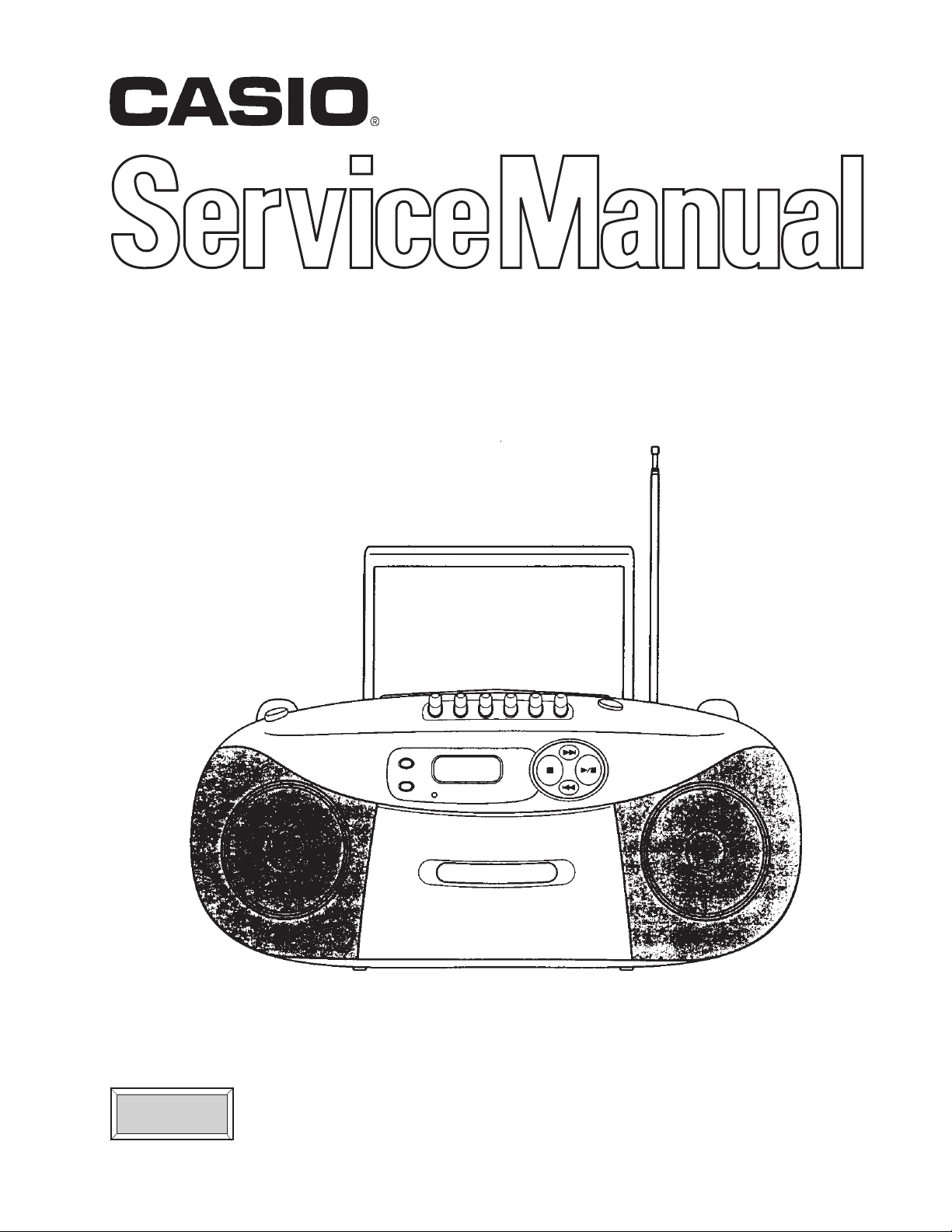
DISASSEMBLY INSTRUCTIONS
1. Remove the battery cover and batteries.
2. Remove six screws A holding case B ass’y(case B unit, PS unit).
Battery Cover
Case B Ass'y
Figure 1
3. Remove four screws B holding the case ass’y.
CD Door
Case Angle
Top Case Ass'y
Case Ass'y
Figure 2
1
Page 5
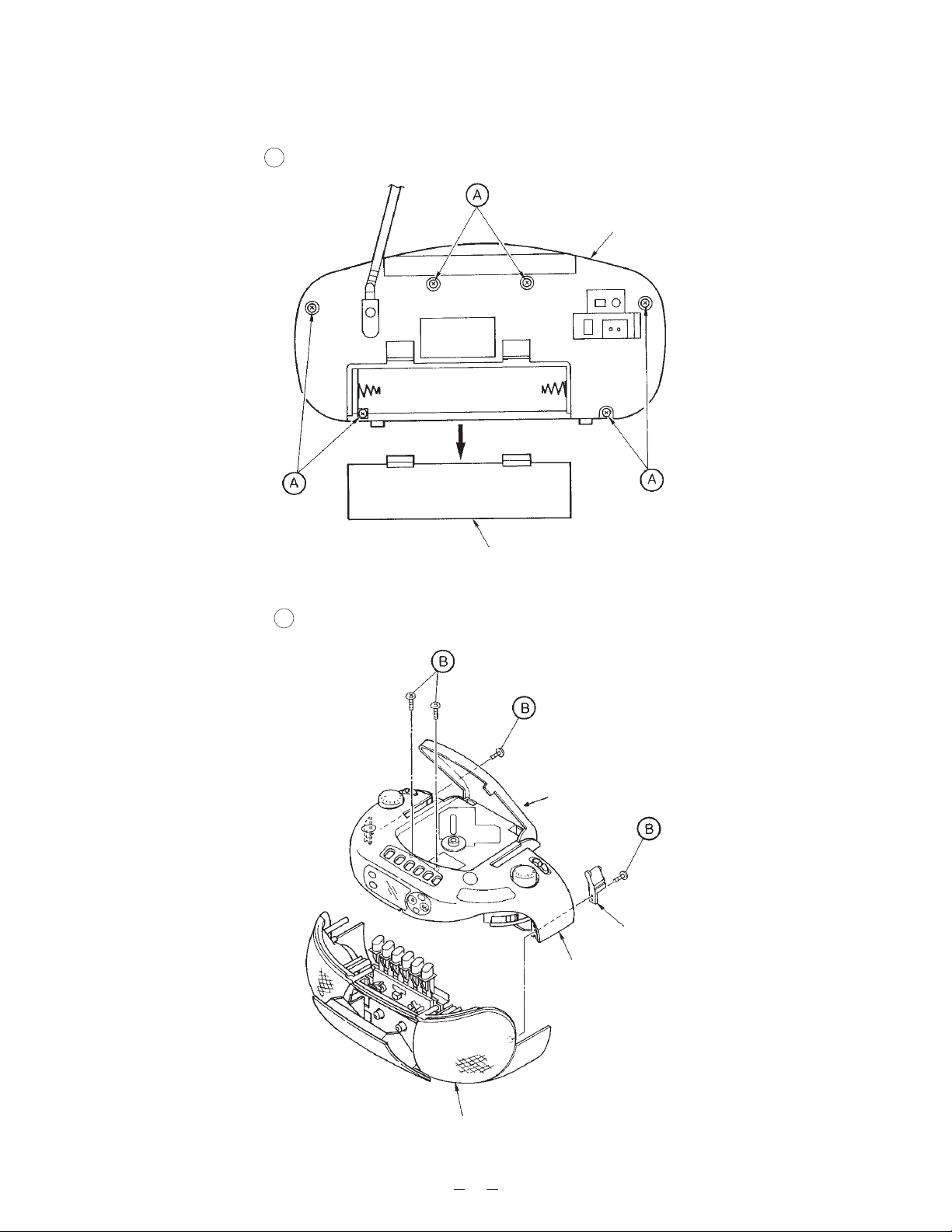
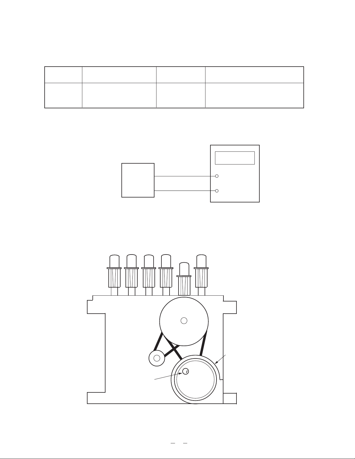
4. Pull out the two slect knobs, volume knob and tuning knob.
5. Remove four screws C holding the tuner unit.
6. Remove six screws D holding the CD AMP unit.
7. Remove five screws E holding the VR unit.
8. Remove three screws F holding the CD mechanism set.
9. Remove two screws G holding the LCD unit.
LCD Unit
VR Unit
Volume Knob
Select Knob
Tuning Knob
Select Knob
Top Case Unit
Tuner Unit
CD
Mechanism
Set
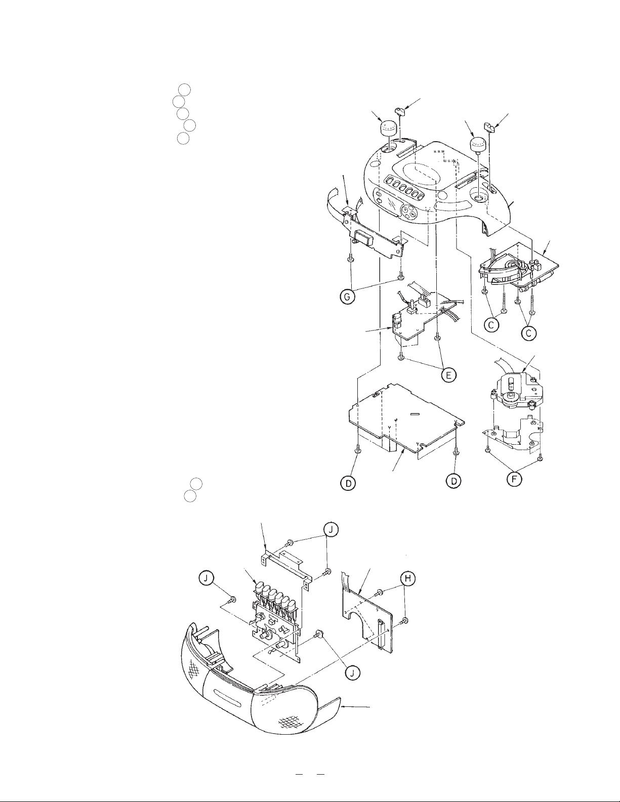
10. Remove three screws H holding the tape unit.
11. Remove four screws J holding the angle A and
cassette mechanism unit.
Cassette mechanism Unit
Angle A
Figure 4
CD AMP Unit
Figure 3
Tape Unit
Case Unit
2
Page 6
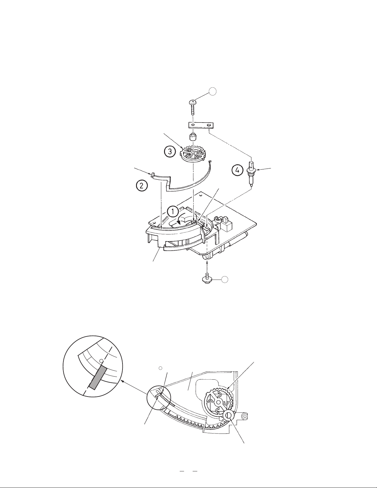
REASSEMBLY OF TUNING POINTER
1. Turn the varicon unclockwise stop position.
2. Set the pointer ; mark position. (refer figure 6)
3. Set the varicon gear of figure 6 position.
4. Insert the tuner gear
Varicon Gear
K
Pointer
Tuner Gear
Varicon
Tuner Chassis
L
Figure 5
Pointer
Mark
Varicon Gear
Tuner Chassis
Tuner Gear
Figure 6
3
Page 7
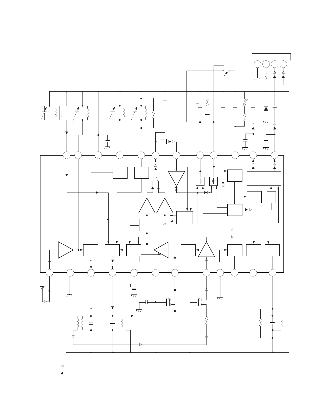
BLOCK DIAGRAMS
Tuner
Antenna
L1 L5
Bar
AM
RF In
FM
RF Out
To Amplifier Block
SW1
AM
BAND SW
FM-MONO
L4
FM
VCC1
22 21 20 19 18 17 16 15 14 1324 23
OSC
FM
OSC
AM
OSC
AM
OSC
L3
DET
Out
MPX In
PRE
FMStereo
LPF1 LPF2
VCO
GND VCC R ch L ch
31 2 4
D3
VCO
Decode
VCC2
FM
AF
CF1
AM/FM
SW
Level
DET
AM IFInFM IF
CF2
F.F
FM
IF
In
TUN
LED
GND2 QUAD
AM
AF
AM
DED
FM
RF
FM
MIX
1 2 3 4 5 76 8 9 10 11 12
Rod
Antenna
FM
RF In
GND1
L7
FM MIX AM MIX
AM
MIX
AGC
L8
AM
IF
AGC
HYS
ST
LEDFMDET
SW
L9
FM Signal
AM Signal
4
Page 8
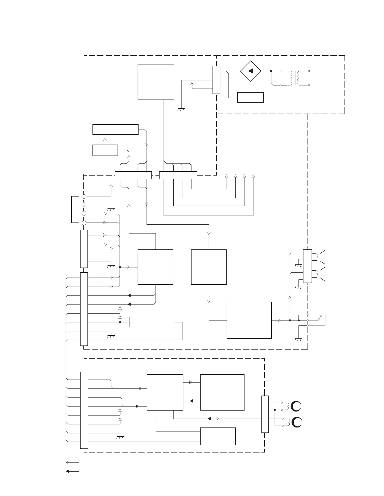
AMP, Tape, PS
To CD
Block
To Tuner
Block
VR201 Volume
SW202
CD 9V
GND
L ch
R ch
L ch
R ch
TU 9V
GND
L ch
R ch
REC L ch
REC R ch
TAPE 9V
DC 9V
GND
BEAT
SW201
Function
Q620,
Q720
SW501 Beat
TU 9V
CD 9V
DC 9V
Tape 9V
DC 9V
GND
AC 9V
Q623,
Q723
AF MUTE
CD 9V
TU 9V
PW AMP
BATT
AMP BLOCK
Tape 9V
DC 9V
IC581
T1
AC
PS BLOCK
Speaker
Headphone
L ch
R ch
REC L ch
REC R ch
Tape 9V
DC 9V
GND
BEAT
Audio Signal
Recording Signal
TAPE BLOCK
SW101
REC/PLAY
IC101
PRE AMP
R/P Head
L101
OSC
5
Page 9
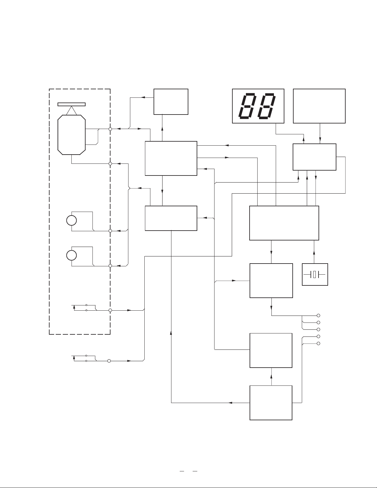
CD
CD Mechanism
Disc
Pickup
Disc
M
Motor
Sled
M
Motor
Q501
Laser
Driver
IC501
Signal Servo
Processor
IC503
Motor and Actuator
Driver
Display
IC502
Digital Signal
Processor
IC504
Audio
Filter AMP
SW801~SW806
Control
IC801
µµ
µ-COM
µµ
X501
16.9 MHz
Pset
SW
Door
SW
CD L ch
A-GND
CD R-ch
CD 9V
Q501, Q511
D510
Regulator 5V
Q504, Q505
D504
Regulator 8V
GND
6
Page 10
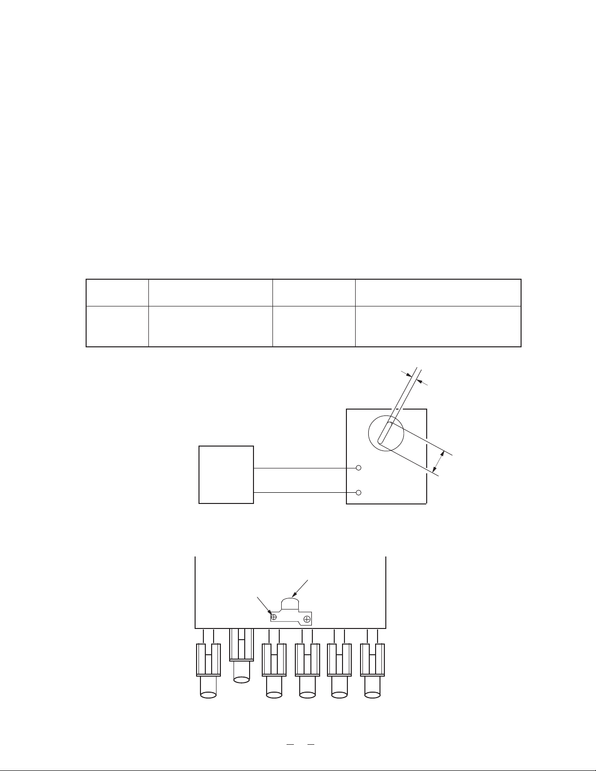
CASSETTE MECHANISM ELECTRICAL ADJUSTMENTS
General Remarks
* Before attempting to adjust the mechanism, wipe clean all tape-contacting surfaces (pinch roller, REC/PB
head, erase head, and capstan), as well as the contact surfaces of the driving parts (motor pulley, flywheel,
pulley, belt, and clutch assembly), with a piece of soft cloth moistened with denatured alcohol. Grease stains
may cause trouble.
* Never use a magnetized screwdriver for head adjustment.
Equipment Required
* Oscilloscope
* Frequency counter
* Screwdriver (Plastic type)
* Test tapes MTT-113C (TEAC) or TCC-111N (TEAC)
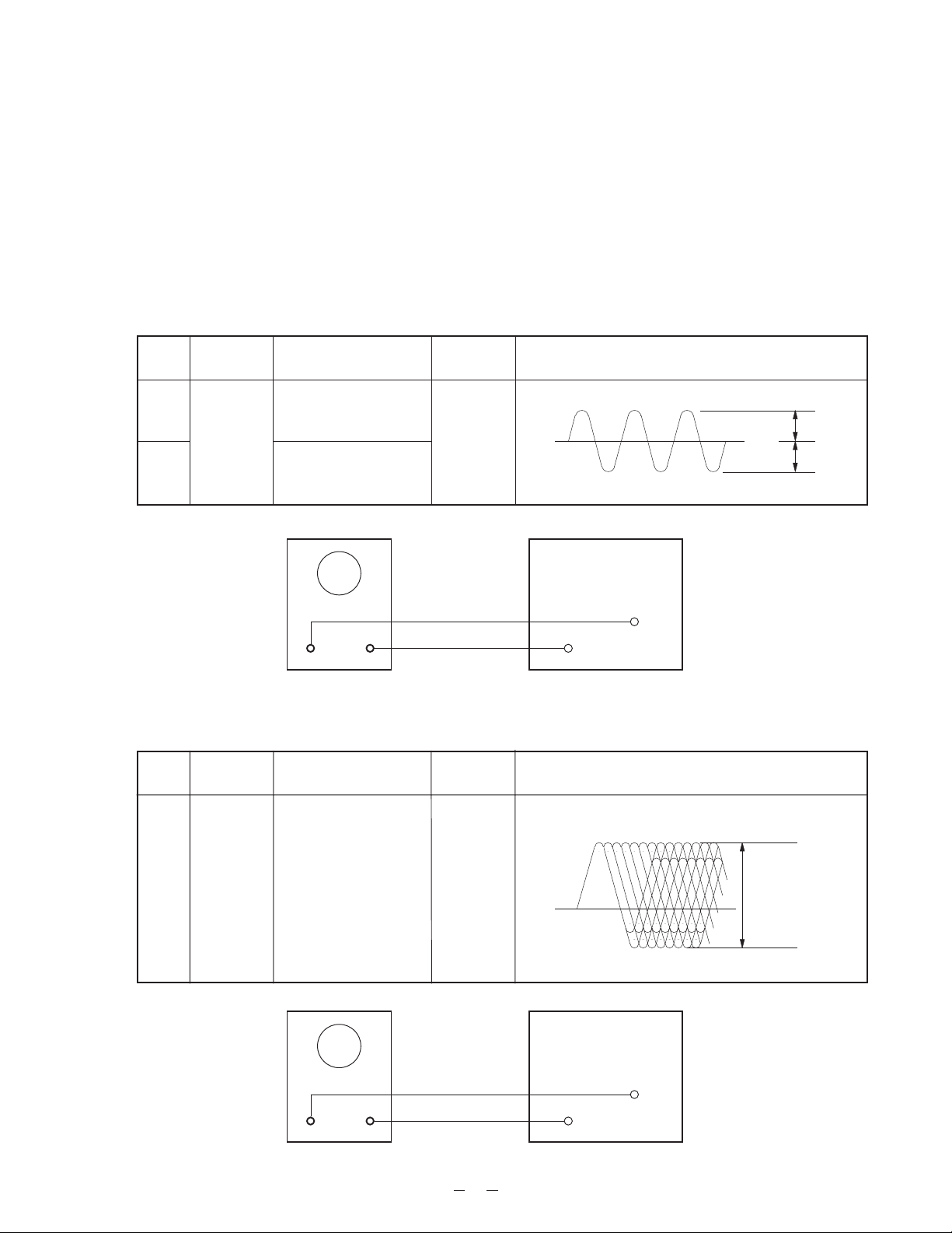
Head Azimuth Adjustment (Figures 7 and 8)
Step Setting
1
Play the test tape 8 KHz
position. (MTT-113C)
Set
Note: Mode Switch is X-Y position.
Adjust Screw
Adjust Result
Azimuth screw
(Figure 8)
J501
Headphone Jack
Figure 7
R/P Head
Obtain the maximum amplitude.
(A: Maximum) (B: Minimum)
B
Oscilloscope
A
Figure 8
7
Page 11
Tape Speed Adjustment (Figures 9 and 10)
Step Setting
1
Playthe test tape.
(MTT-111N)
Set
Adjust
Motor screw
(Figure 10)
J501
Headphone Jack
Figure 9
Result
Frequency counter reading
should be 3000 Hz (2910~3090).
Furequency Counter
3000
screw
Motor
Figure 10
8
Page 12
CD ADJUSTMENTS
Pre-Adjustment Procedures
* Remove the bottom chassis assembly. (Refer pages 1, 2)
* Use the plastic screwdriver.
Equipment Required
* Syncroscope (with probe 10:1)
* Screwdriver (Plastic type)
* The Test Disc SONY YEDS-18(Type 4)ABEX TCD784
E-F Balance Adjustment (Figures 11 and 13)
Step Connect Setting Adjust Result
Play the test disc.1
2
See
Figure 11
Set the PAUSE
mode.
Syncroscope CD PCB
VR501
A=B
0V
(Vref)
A
B
R572
(TSO)
GND
R571 Vref
Figure 11
RF Adjustment (Figures 12 and 13)
Step Connect Setting Adjust Result
1
See
Figure 12
Play the test disc.
VR502
Adjust VR502 for the amplitude of the waveform
at maximum.
0V
Measuring on syncroscope.
Syncroscope
CD PCB
>1.0V p-p
GND
Figure 12
9
R570 (RFO)
R571 Vref
Page 13
CD Adjustment Points
Vref
R571
RFO
R570
TSO
R572
VR502
RF
VR501
EF Balance
CD PCB Top View
Figure 13
10
Page 14
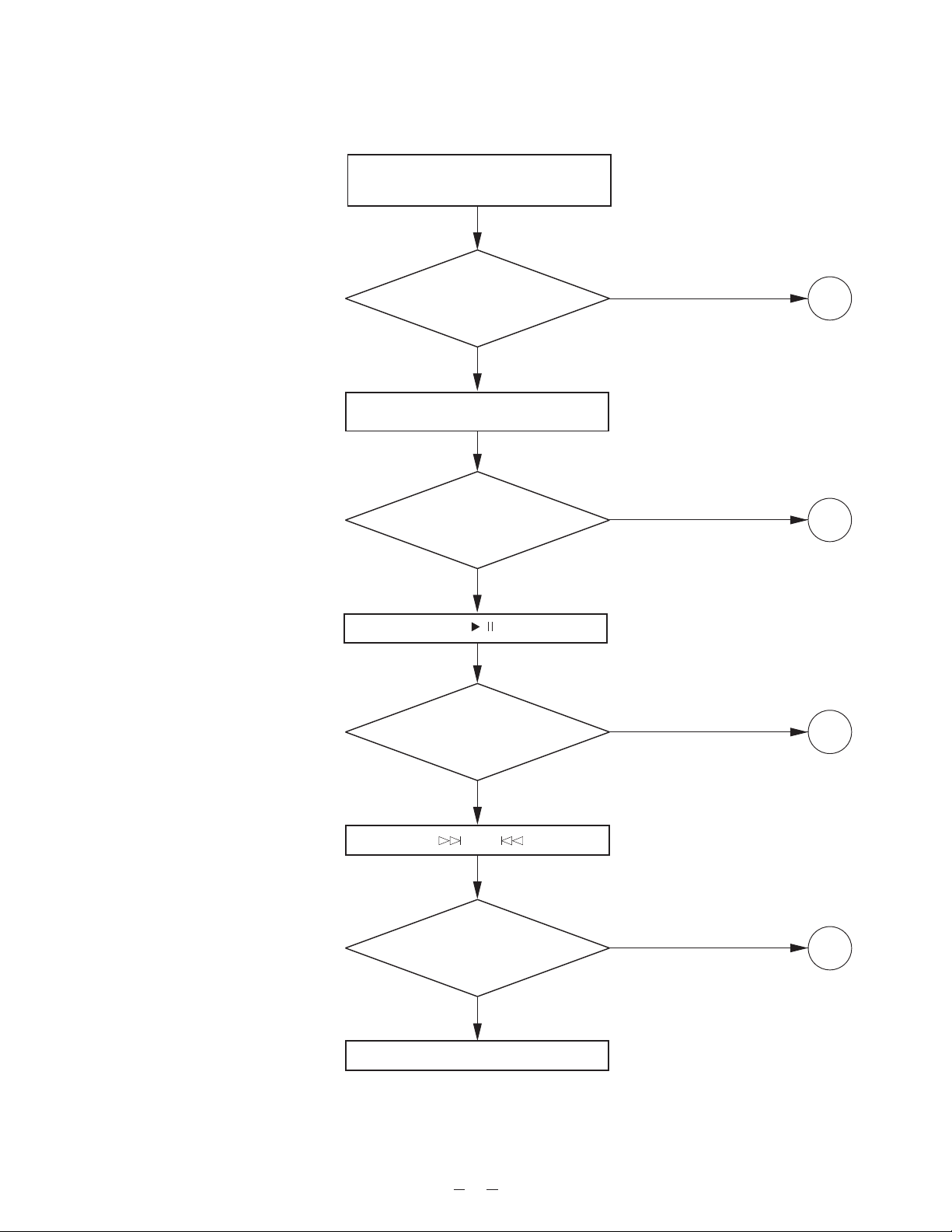
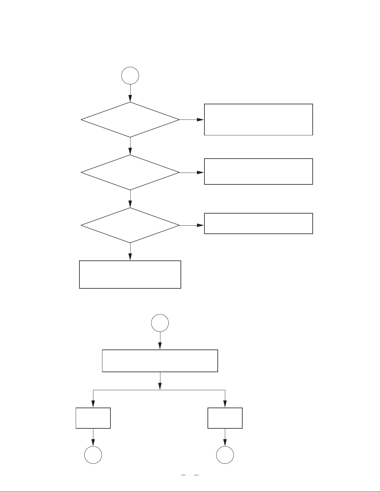
CD TROUBLESHOOTING
Open CD door and set function switch
for CD position.
Is “00” display
on LCD ?
Yes
Load a disc and close CD door.
Is total track
numbers displayed about 5
seconds ?
Yes
Press “ / “ key.
Is the audio signal
present at the output
terminals ?
No
1
No
2
No
3
Yes
Press “ “ or ” “ key.
Can a selected
of music be searched
smoothly ?
Yes
OK
11
No
4
Page 15
1. At power on, “00” is not displayed.
1
Is +5 V lines normal
(for IC801)?
Yes
Does 16.93 MHz
clock pulse appear at
IC502 pin 79 ?
Yes
Does 1.4 MHz
clock pulse appear at
IC801 pin 30 ?
Yes
* Check and circuit around IC801.
* Check LCD.
* Check wire connector.
No
No
No
* Check Q510, Q511 and D510.
* Check Q504, Q505 and D504.
* Check circuit around IC801.
* Check X501.
* Check circuit around X501 and IC502.
* Check circuit around IC502 pin 72.
2. “-- --” is not displayed total track numbers.
2
How long times it takes until “-- --” is
displayed after CD door has closed.
About
5 sec.
A B
12
About
16 sec.
Page 16
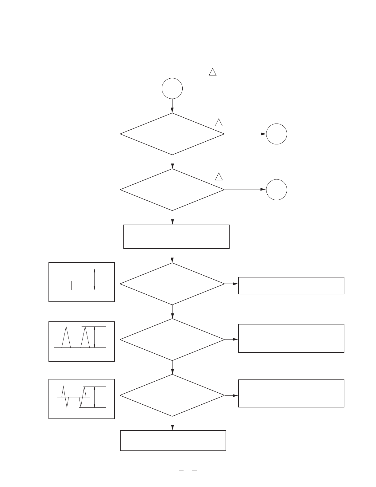
2-A
A
Does the LASER emit ?
Yes
Dose the lens move
up and down ?
Yes
Load a disc and close CD door.
Then check the following.
Note: Open the CD door and check the radiation
!
power with an optical power meter or by watching
the radiaation through the lens of the pickup unit at
a minimum distance of 30cmfrpm the pickup.
!
No
A1
!
No
A2
SEL-GND
Figure 14
RFO-Vref
Figure 15
FEO-Vref
Figure 16
5V
1V
>0.4V
Is the waveform
at pin 21 (SEL) of IC501 like
that shown in Fig. 14 ?
Is the waveform
at R570 (RFO) like that
shown in Fig. 15 ?
Is the waveform
at pin 10 (FEO) of IC501 like
that shown in Fig. 16 ?
* Check around IC501.
Yes
Yes
Yes
No
* Check around IC501 and IC502.
* Check wire connector from pickup.
No
* Check IC501.
* Check pickup.
* Check around pins 8, 9 and 10 of
No
IC501.
* Check VR502.
13
Page 17
2-A1
A1
(GND)
Figure 17
(GND)
Figure 18
5V
0V
5V
2.5V
0V
Is Q501
emmiter 5V ?
(Play)
Yes
Are waveforms at
pins 14~19 of IC502 like that
shown in Fig. 17 ?
Yes
Is waveform
at pin 42 (SEL) of IC502 like
that shwn in Fig. 18 ?
Yes
No
No
No
* Check Q501.
* Check around IC 502 and IC801.
* Check around IC501 and IC502
(SEL).
(GND)
Figure 19
3V
0V
Is waveform at
base of Q501 like that
shown in Fig. 19 ?
* Check 16P flat cable.
* Check pickup.
Yes
14
No
* Check around pin 45 of IC501
and Q501.
* Check IC501.
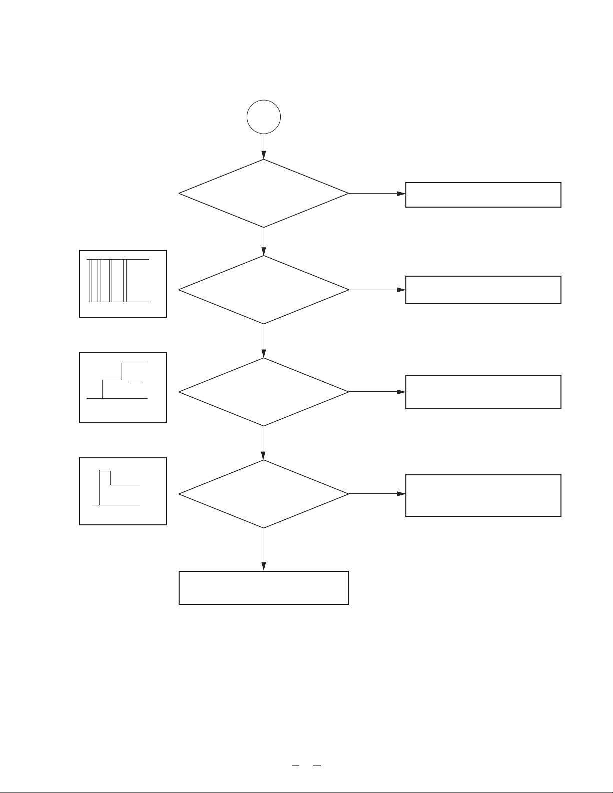
Page 18

2-A2
A2
Are voltages more
than 8V appeared at pins
1and 10 of
IC503 ?
Yes
Is waveform at
pins 11 to 12 of IC503 like that
shown in Fig. 20 ?
Yes
* Check 16P flat cable.
* Check pickup.
No
No
* Check around IC503 and Q504.
Is waveforn at
pin 16 (FSO) of IC501like
that shown in Fig.21 ?
Yes
No
pin 17 (COSC) of IC501 like that
* Check around IC503.
* Check around IC502.
* Check around IC501.
VREF-FSO
4V
Figure 20 Figure 22
Figure 21
1V
Is waveform at
shown in Fig. 22 ?
Yes
VREF-COSC
15
No
1V
Page 19

2-B
B
Figure 23
> 5V
>4V
Does the
disc motor rotate ?
No
Is waveform at
pins 15 to 16 of IC503 like that
shown in Fig. 23 ?
Yes
Is waveform at pin
40 (DMPC) of IC502 llike that
shown in Fig. 24 ?
Yes
Yes
No
No
B1
* Check wire connector CN543 and
wire.
* Check disc motor.
* Check around IC501 and IC502.
Figure 24
Is waveform at pin
24 (DMEO) fo IC501 like that
shown in Fig. 24 ?
Yes
* Check around IC501 and IC502.
16
No
* Check around IC501 and IC503.
Page 20

2-B1
B1
Confirm the waveforn at R570 (RFO) with a
syncroscope.
Waveform Waveform
B2
Is waveform at
pin 53 (RFI) of IC502 like that
shown in Fig. 25 ?
Yes
Is waveform at
pin 60 (PDO) of IC502 like that
shown in Fig. 26 ?
Yes
* Check digital signal of IC502 and
IC801.
* Check IC502 and IC801.
No
No
* Check around pin 53 of IC502.
* Readjust VR502.
* Check around PLL of IC502.
Figure 25
1.0~1.4V
4V
Figure 26
17
Page 21

2-B2
B2
Is waveform R572
(TSO) like that shown
in Fig. 27 ?
Yes
Is waveform at pin
30 (TS20) of IC501 like that
shown in Fig. 27 ?
Yes
Is waveform at pins
13 to 14 of IC503 like that
shown in Fig. 28 ?
Yes
* Check pickup.
No
No
No
* Check 16P flat cable.
* Readjust VR501.
* Check IC501.
* Check around TE-Amp lines.
* Check IC501.
* Check around TSO lines.
* Check IC503.
0.6V/1.5V
3V
3. No present at output terminals audio signal
3
Does audio
signal appear at IC504
pins 1 and 7 ?
No
* Check D601 and D701.
* Check around IC601.
Yes
18
Figure 27 Figure 28
* Check around IC502 pins 2~6 and IC504.
Page 22

4. Selected of music cannot be searched.
4
Press the play key.
(PAUSE)
VREF-TSO
Figure 29
VREF-TSO
A
B
Figure 30
VREF-FMFB
Figure 31
Vref
Vref
VREF
A=B
A+B=0.6V<
Is waveform at
R572 (TSO) like that
shown in Fig. 29 ?
No
Is waveform at
R572 (TSO) like that
shown in Fig. 30 ?
No
Press the” “ or “ “ key.
Is waveform at
pin 36 (FMFB) of IC502 like
that shown in Fig. 31.
No
Yes
Yes
Yes
* Readjust VR501.
* Check wire connector CN502.
* Check pickup.
* Check around IC503.
* Check sled motor.
VREF-TKIC
Figure 32
Is waveform at
pin 33 (TKIC) of IC502 like that
shown in Fig. 32 ?
No
* Check around pins 36 and 33 of
IC502.
19
Yes
* Check around IC501.
Page 23

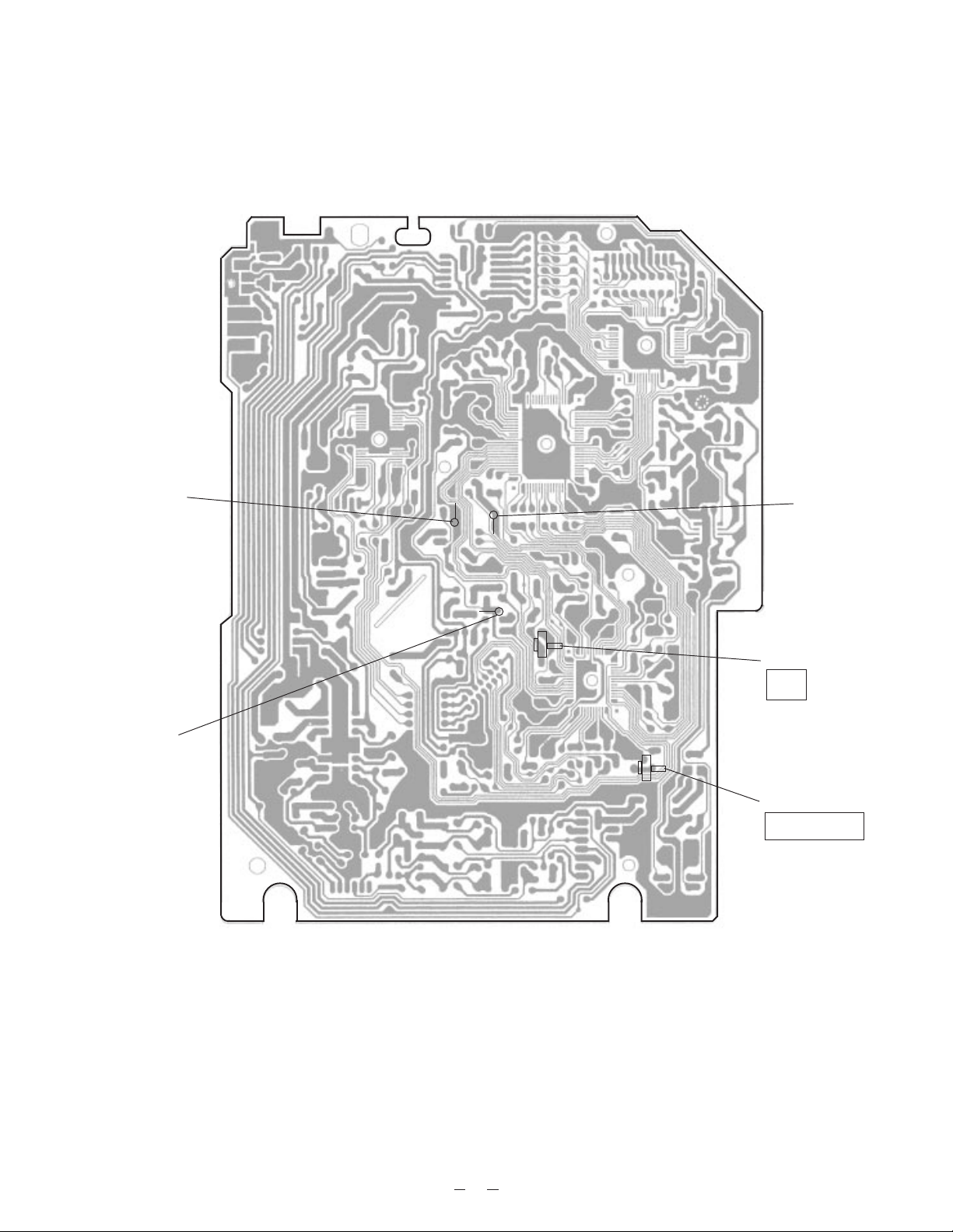
Tuner PCB Top View
PCB VIEWS
20
Page 24

CD AMP PCB Top View
Door Switch PCB Top View
21
Page 25

VR PCB Top View
22
Page 26

PS PCB Top View
AC-1
AC-2
CN400
F400
FUSE : 1.6A/125V
AC9V
GND
DC9V
PS PCB
C2451-505-0-91
D401
D403
C401
C403
BATT-2
BATT-1
JP400
JP401
C400
D402
C402
C404
D404
23
Page 27

Tape PCB Top View
24
Page 28

LCD PCB Top View
25
Page 29

CASSETTE MECHANISM
WIRING DIAGRAM
Red
Switch
R/P Head
Yellow
White
Red
(No.159)
Shield
(No.151)
Shield
White
Yellow
Motor
TAPE PCB
PS PCB
LCD PCB
1
6
1
3
8
1
(No.152)
(No.244)
No.342
1
1
4
TUNER PCB
(No.353)
Batteries 1.5 x 6
3
Shield
2
1
1
9
Red
Trelescopic
Antenna
White
1
2
White
Red
Shield
21
(No.221)
(No.289)
(No.243)
Red
Shield
White
Red
White
Shield
No.268
1
1
6
4
CN548
No.204
No.248
(No.241)
CN551
1
8
CN540
CD AMP PCB
CN539
16
1
1
4
10
1
CN543
(No.264)
CN547
8
CN546
2
1
8
1
(No.265)
CN544
1
10
1
1 2
1 2
19
CN542
Power Transformer
Yellow
Yellow
Brown
Blue
(No.352)
(No.352)
AC Socket
12
Pickup
16
1
Bar Antenna
CD MECHANISM
2 1
Preset
Switch Disc Motor Sled Motor
26
14
(No.335)
(No.186)
(No.195)
No.205
(No.311)
14
Speaker L ch Speaker R ch
(No.201)
DOOR SW PCB
1 2
Page 30

IC3: TA8167N
IC LEAD IDENTIFICATION AND INTERNAL DIAGRAMS
24
13
FM
12
AM
AM
DET
AM
IF
DET
Out
MPX In LPF1 LPF2 VCO L ch Out R ch Out
FM
AF
PRE
AM/FM
SW
Level
DET
FM
IF
VCO
F.F
TUN
LED
HYS
ST
LED
VCC1 FM OSC AM OSC
22 21 20 19 18 17 16 15 14 13
FM
MIX
FM
OSC
AM
MIX
OSC
AM
AF
AGC
Decode
SW
FM
DET
1
AM
RF In
RF Out
24 23
FM
RF
1 2 3 4 5 76 8 9 10 11 12
FM RF In GND1 FM MIX AM MIX AGC VCC2
AM IF In
FM IF In
GND2 TUN LED
IC101: TA7668BP
16 9
1
NF
R In
ALC
L In
NF
10
11
8
6
PRE
7
8
ALC DET
PRE
R Out REC Out Out Mute In
5 4
REC
REC
15
3
ST LED QUAD
16
V
CC
2
VS
27
1149 12 13
MuteREC OutL OutGND
GND
Page 31

IC501: TA2065F
39
2538
24
48
114
RFT RFN MDI LDO FPI FNI TNO TNI TPI TPO
48 47 46 45
500
22k
47k
1
RFO
RFI
VRO
2VRO
RFRP
SBAD
DFIN
FEP
FEN
FEO
FEI
FHLD
FEL1
FEL2
2
3
4
5
6
7
8
9
10
11
12
13
14
49k
22k
70k
30k
RF
VR
2VR
33P
20k
21k
21k
33P
30k
150k
15
FSN FSO COSC OSCI GND V
15
20k
RFBF
21k
21k
21k 29k
FE
100k
16
5k
FS
47k
15k
15k
44
PEAK
BOTTOM
16k
1.27k
1.5k
FP FN
2.5µA
20k
13k
3.5µA
5k
16k
20k
RFRP
FSOSC
17
43 42 41 40 39
30k 30k
ADD
680
MD
DET
3 STATE
16k
CC
39P
TN
10k
20k
20k20k
TE
20µA
25k
TS
TS1
1k
LD
47k
100µA
21201918
SEL
2.8k
BGR
10k
1.35V
68k
22
DMEP DMEN DMEO
20k
20k
68P
24k
12k
100k
DM
23
10k
TS2
FMS
5P
68k
39P
10k
TP
10k
24
7k
17.5k
47k
47k
20k
180k
38
37
36
35
34
33
32
31
30
29
28
27
26
25
TSN
TEL2
TEL1
TSO
TS1P
TS1N
TS2P
TS2N
TS2O
THLD
FMSP
FMSN
FMSO
DFCT
28
Page 32

IC502: TC9284BF
65
4164
40
2VREF
SEL
FCSI
FKIC
FEL2
FEL1
FEI
TESH
TEOF
SBAD
RFRP
VREF
RF1
GNDA
DTSC2
MONIT
DTSC1
VDDA
PDCNT
PDO
TNAX
LPFN
LPFO
VCOF
41
42
43
44
45
46
47
48
49
50
52
53
54
55
56
57
58
59
60
61
62
63
64
51
80
124
DMPC
DMFC
DMON
TEST
FMFB
TEST1
FMON
TKIC
TGUH1
40 39 38 37 36 35 34 33 32 31 30 29 28 27 26 25
Focus/Tracking Servo Tracking Search
A/D Converter
Data Slicer
PLL Circuit
Control Circuit
Servo Status Signal
Generating Circuit
16 K RAM
Address Circuit
CLV Servo Circuit
TMAX Detection Circuit
Circuit
Circuit EFM
Demodurarion
SYNC Separation
Crrection
Output Circuit
(Audio Output)
Correction
TGUH2
Circuit
Digital
25
TGUL
Out
TEL1
TEL2
DFCT
Correction
Sydtem
Timing
Generator
Control Data Bus
Q Data
Subcode
Clock
DA
Converter
GNDD
Interface
Storage
Demodulation
Generator
VDDD
RAM
24
23
22
21
20
19
18
17
16
15
14
13
12
11
10
9
8
7
6
5
4
3
2
1
CLCK
SUBD
SUBSYC
RST
4MCK
BUCK
CCE
BUS3
BUS2
BUS1
SUS0
GNDD
VDDD
SBOK
TEST5
TEST4
TEST3
GNDA
LO
LO
VDA
RO
RO
GNDA
Internal
Status
65 66 67 68 69 70 71 72 73 74 75 76 77 78 79 80
VDDX
XI
XO
HS
TESTX
GNDD
SPDA
COFS
CHCK
WDCK
BCK
AOUT
EMPH
DOUT
TEST2
29
GNDX
Page 33

IC503: BA5941FP
28 15
1
VIN4’ VIN4 VIN3’ VIN3 OP Out OP In(-) OP In(+)
27 26 25 24 23 22 21 20 19 18 17 16 15
28
10K
10K
14
GND NC VCC VO3(-) VO3(+) VO4(-) VO4(+)
13.3K
Level shift
13.3K
Level shift
Level shift
13.3K
13.3K
10K
1
V
BIAS In VIN1’ VIN1 VIN2’ VIN2 GND GND MUTE VCC VO2(-) VO2(+) VO1(-) VO1(+)
CC
3 4 5 6
2
10K
7
MUTE
8
9 10
Level shift
11 12 13 14
IC504: BA4510F
85
14
CC
+In 2-In2Out 2V
8 7 6 5
2
1
1 2 3 4
Out 1 -In 1 +In 1 V
30
EE
Page 34

IC581: TA8227P
12
16
Vcc1
Vcc2
7
B.S. 1 Out 1 Power GND
3 4
2
12
Ch 1
1
6
In 1 NF 1
30 kΩ
45Ω
5
Bias Circuit
Thermal
Shut Down
Protection
Circuit
9
Ripple
OUt 2
11 10
30 kΩ
Ch 2
8
7
In 2 NF 2
45Ω
B.S. 2
Pre GND
(F In)
31
Page 35

IC801: TMP47C422F-FR11
Segment drive output Common drive output
Power
Supply
V
DD
V
SS
LCD Drive
Power
Supply
VLC
COM1
COM2
COM3
COM4
V
DD
SEG0
SEG1
SEG2
SEG3
SEG4
SEG0~SEG4,
SEG5~SEG11
HOLD (KEO)
RESET
XOUT
XIN
P51
P50
R92 (SCK)
3332313029282726252423
34
35
36
37
38
39
40
41
42
43
44
1234567891011
SEG5
SEG6
SEG7
SEG8
SEG9
SEG10
SEG11
SEG0~SEG4,
SEG5~SEG11
LCD DriverVLC
R91 (S0)
R90 (S1)
R83 (T1)
R82 (INT1/ZIN)
22
21
20
19
18
17
16
15
14
13
12
R60 (SEG12)
R61 (SEG13)
R62 (SEG14)
R63 (SEG15)
R81 (T2)
R80 (INT2)
R73 (XOUT)
R72 (XTIN)
R71 (PULSE)
R70
V
SS
R43 (AIN3/SEG19)
R42 (AIN2/SEG18)
R41 (AIN1/SEG17)
R40 (AIN0/SEG16)
(Segment drive output)
I/O Port
Analog input
R4 R6
I/O Port
(Segment
drive output)
R60~R63R40~R43
Hold Input
Hold (KEO)
Reset Input
RESET
Test Pin
TEST
XIN
XOUT
OSC
connecting
pins
KE
Flag
C Z S
Hold Controller
System Controller
System Clock
Controller
Timing Generator
High
Frequ.
Low
Frequ.
R70~R73
Clock
Generator
R7 R5
I/O port
(OSC. connecting
pins)
ALU
Interval-
Watchdog
P50, P51
I/O port
Accumulator
EIR EIF
Interrupt Controller
timer
Timer
Zero-
cross
(T/C input)
(Interrrupt input)
HR LR
RAM
Address
Buffer
12-bit
Timer/
Counters
(2 ch)
R8 R9
R80~R83
Interface
I/O port
(Serial port)
8-bit
Serial
R90~R92
I/O port
Data Memory
(RAM)
LCD Display
Data Area
Stack SPW
TC1 TC2 DC
8-bit
A/D
Converter
Program
Counter
Program
Memory
(ROM)
IR
Decoder
32
Page 36

CD Mchanism
SCHEMATIC DIAGRAMS
Disc
1
2
3
4
6
7
8
9
Sled
Motor
Disc
Motor
10
11
12
13
5
14
15
16
M
M
P set
Switch
33
Page 37

Tuner
D2
1SS133
C10 33PF
L6
C9
15PF
ANT1
ROD ANT
C26
0.022
D6
1S2234-10
C3
C7
0.022
R2
100K
5PF CH
C6
0.022
PVC AM-ANT
FM-DFT
AM-DFT
0
0
1
4
R
CF2
FFE1070MA
C28
C32
0.022
100/16
FM-OCT
CF1
FFD455MB
5
R
4.7K
FM-ANT
L7
L8
C11
C12
33/10
C30
22PF
0.047
L9
1
2
3
4
5
6
7
8
9
10
11
12
IC3
TA8167N
FMI
GD1
FMM
AMM
AGC
VCC
ATF
FIF
GD2
TL
SL
QUD
AMR
24
23
FMR
VC1
22
21
FOS
AOS
20
19
DET
18
MPX
17
PF1
16
PF2
15
VCO
LO
14
13
RO
C23 0.018
C22 0.018
PVC FM-RF
C4 18-27PF
R1 33
C14 10/10
(22PF)
L5
FM-RF
C15
0.33/50
C16 3.3/25
C17 0.1
C21 1000PF
R8 12K
CH
C1 22PF
BZX55-C51V
C2 18-27PF
CH
R7 1K
SVR1
10K (B)
D3
C20
0.022
(22PF)
L4
FM-OSC
C13
C8
0.022
1000PF
R3 10
PVC FM-OSC
R6 1M
CH
(5PF)
R13 56K
FM-S
L1
AM BAR-ANT
L3
AM OSC
C5
3-12PF
PVC AM-OSC
AM
FM-M
R11
220
1/2W
C25 3300PF
C24 3300PF
D5
1SS133
R10 15K
R9 15K
D4
1SS133
C19
100/16
C18 1000PF
BAND SW
SW1
Notes:
1. All resistance values are in ohms (k=1000 ohms, M=1000 kohms).
2. All capacitonce values are in uF (P=10 uF).
4
JP M
PJ4
1
2
3
3. All resistors are 1/6 watt, unless otherwise specified.
-6
34
Page 38

AMP, PS
*This circuit diagarm shows the basic circuit.
It is subject to change for the purpose of important.
*Parts maker with
in respect to the safety.
Use the specifed type without fail.
are of importance
2446-548
2.0pitch
CW552
DECK MECHA
6
5
4
3
2
1
TO
TUNER
TAPE
PCB
C211
10u
16V
R207
10K
BBS
0.1
0.1
CON4
2.5
551
1
2
3
4
5
6
7
8
C650
C750
CN551
1
2
3
4
1
2
3
4
5
6
7
8
(M)
(M)
CN540
8pin
2.5pitch
CN547
1
1
2
2
3
3
3pin
2.0pitch
L ch
R ch
TU 9V
GND
L ch
TAPE 9V
R ch
DC 9V
REC Lch
GND
REC Rch
BEAT
C594
B 0.001
Rch VO
Lch VO
GND
Rch VI
Lch VI
L
c
h
SW501
W_SLIDE_SW
3
2
2
3
to LCD PCB
BLOCK
R
c
h
VR201
'
'
VR XVO
TO
CD
A
G
N
D
C720
R720
22K
0.027u
0.027u
R620
22K
C620
BEAT CUT SW
50V
C722
C736
C636
C622
50V
50V
'
1
1
C205
0.047
(F)
2
1
3
2
1
CN546
C
T
1K
R723
1K
R623
1K
Q620
R622
1K
C723
0.47u
C623
0.47u
T
D
U
A
N
P
9
E
E
V
R
9
9
V
V
50V
50V
9pin
2.0pitch
C
D
A
D
C
G
9
N
9
V
D
V
R722
R721
560K
1u
Q720
C721
2SC1815
220P
(B)
1u
50V
(M)
(M)
1u
C621
220P
(B)
2SC1815
R621
560K
1u
R652
R752
1.8K
R651
3.3K
1.8K
2451-551
2.5pitch
CW540
2446-540
2.5pitch
CW547
2446-547
2.0pitch
SW202
CW551
1
2
3
4
1
SW
MOTOR
2
4.7K
R650
R751
R750
3.3K
4.7K
TO:DOOR SW PCB
43
4 5
TA
CD
TU
TA
CD
TU
TU
CD
TA
SW201
TU
FUNC SW
CD
TA
C210
0.047
(F)
87
65
8 9
6 7
A
D
G
N
F
C
N
.
D
C
M
9
U
V
T
E
(B)
C806
1000
C203
2200u
16V
D201
1N4148
CW548
2446-546
9
2.0pitch
C595
F0.047
A
C
9
V
R579
2.2K
VOL PCB
C212
F0.047
F0.047
C202
2
1
C2446-545
C580
220u
16V
CW549
2451-549
2.5pitch
CD AMP PCB
R590
100K
C588
22u
C729
R734
R634
4.7K
C629
R
L
L
R
c
c
c
c
h
h
h
h
G
V
V
V
V
N
O
O
I
I
D
2.0Pitch
6
54
3
21
5 6
3 4
1 2
TO VOL PCB
CN400
DC 9V
1
1
GND
2
2
AC 9V
3
3
CON3
2.5
549
PS PCB
16V
R733
2.2K
4.7u
50V
4.7K
Q723
2SC1815
Q623
2SC1815
R633
2.2K
4.7u
50V
CN548
6PIN
(B)
470P
C730
(B)
470P
C630
C400
3300u
16V
C732
22u
16V
R735
C731
100P
IC581
C631
100P
CH
C632
22u
16V
BT
BATTERY
C401
0.01
D401
1N4001
D403
1N4001
C403
0.01
2
C402
0.01
D402
1N4001
D404
1N4001
C404
NOP
1
F400
FUSE
BATT-1
AC
BATT-2
T1
3
AC-2
4
TRANS
AC-1
2
4
5
1
1
2
2
AC
3
J301
PLUG MALE
120V 60Hz
(CT-1219U)
1
T1.6A/125V
CN542
4pin
2.5pitch
C590
470u
16V
47
R591
(1/4W)
C734
270
270
C589
4
PREGND
RPL
9
10V
47u
C733
13
PWGND
TA8227P
PWGND
14
C633
CH
5
6
IN1
NF1
IN2
NF2
8
7
R635
3
B.S.1
B.S.2
10
10V
100u
10V
100u
2
OUT1
OUT2
11
1000u
10V
1
VCC2
VCC1
12
C635
C634
1000u
10V
270
(M)
C735
0.15
R736
L CH
R CH
EM501
EM502
EM503
270
16V
1000u
0.15
(M)
C592
R636
SPEAKER
CW542
1
1
2
2
3
3
4
4
2451-542
2.5pitch
J501
H.P JACK
SP1A
1
2
3
4
L
LEFT
SP1B
R
RIGHT
Notes:
1. All resistance values are in ohms (k=1000 ohms, M=1000 kohms).
2. All capacitonce values are in uF (P=10 uF).
-6
3. All resistors are 1/6 watt, unless otherwise specified.
35
Page 39

R120
220K
R121
220K
R104 20K
C104
0.0027u(B)
C103
0.01u
(M)
R103
1K
R102
1K
C102
0.01
(M)
R105
10K
R107
220K
C107
22u
16V
C106
1u
50V
R109
6.8K
R122
1K
C105
0.01u
(M)
R106
82
C135
47p(CH)
C126
0.001u
(M)
C127
0.0047u
(B)
D103
1N4148
C132
1u
50V
R126
100K
R125
47K
C129
47u
16V
12
C130
100u
16V
C140
100u
16V
C128
1u
50V
C111
220p
B
C111
220p
B
C111
220p
B
C111
220p
B
C111
220p
B
C111
220p
B
C111
220p
B
345678
R108
68K
A
L
C
I
NMFOU
T
R
E
C
O
U
T
M
U
T
E
VSG
N
D
P
R
E
GINNF
O
U
T
O
U
T
M
U
T
E
M
U
T
E
I
N
V
C
C
IC101
TA7668BP
C108
10p
(CH)
C111
220p
(B)
R101
220K
C110
47u
16V
C101
4.7u
50V
C109
0.0022u
(M)
H
I
SW101
F
E
G
C113
4.7u
50V
C112
0.0022u
(M)
R124
1K
R114
220K
C116
1u
50V
C114
22u
16V
R110
68K
C118
1u
50V
9 10 11 12 13 14
C136
47p(CH)
C119
0.0047u
(B)
C121
220p
(B)
C117
10p
(CH)
R130
4.7K
C133
10u
16V
R127
100K
R128
47K
R129
10K
15 16
R123
100
1/4w
L ch
TAPE 9V
R ch
DC 9V
REC L ch
GND
1
2
3
4
5
6
7
8
JP F
PJ 8
REC R ch
BEAT
C134
1u
50V
D104
1N4148
R115
20K
R111
82
C115
0.01u(M)
C131
0.01u
(M)
C120
0.0027u
(B)
R113
10K
C
D
TL
R/P L
GND
4
3
2
1
JP G
1
2
3
4
JP G
R/P R
R/P COM
1
2
3
4
R/P HEAD
A
B R112
6.8K
R119
220
1/4
R116
8.2
R132
10K
Q101
2SC1815
C124
0.01u
(M)
R117
100
C125
220u
16V
D105
RD3.0B
L101
MT216-1188
Q102
2SC1815
R131
4.7K
C122
0.0022u
(PR)
C138
0.0022u
(PR)
C137
0.0082u
(PR)
Tape
36
Notes:
1. All resistance values are in ohms (k=1000 ohms, M=1000 kohms).
2. All capacitonce values are in uF (P=10 uF).
-6
3. All resistors are 1/6 watt, unless otherwise specified.
Page 40

LCD PCB
1
2 3
4 5
6 7 8
9 1
0
U1
2446LCD
1 2
3 4
5
6 7 8
910
CN544
10pin
2.0pitch
1
0
987
6
54
321
CW544
2446-544
2.0pitch
2
1
2446-550
DOOR SW
TO:CD AMP PCB
C594
2
1
CW551
2446-551
Pitch2.5
1 2
CN500
P2.5
P-SET SW
P-SET SW
CD MECHA
L501
10uH
Q501
2SA1015
R510
22
1/4
C502
100u
10V
+5V
C543
0.047u
(F)
R511
51K
R512
39K
R514
680K
R529
1.5M
CD AMP PCB
R531
47K
R530
1K
R536
33K
R533
1.8K
R532
2.2K
C517
220
10V
R561
100K
R562
10K
C518
0.1u
(M)
C519
0.022u
(M)
C520
0.1U
50V
C521
0.033u
(M)
VREF
TP
TSO
(TE)
R572
1
TSO
(TE)
R534
1.2M
R535
15K
D
G
N
D
R841
10K
R842
10K
RR843
560K
D803
1N4148
V
L
C
3
4
C
0
3
5
C
1
3
6
C
2
3
7
3
8
V
D
D
3
9
S
0
4
0
S
1
4
1
S
2
4
2
S
3
4
3
S
4
4
4
33
S5
1
P-SET
11
NEXT
10
TEST
9
DOOR OPEN
8
7
6
5
4
3
S6
2
S
T
D
B
Y
1
2
M
U
T
E
1
3
B
U
C
K
1
4
C
C
E
1
5
V
S
S
1
6
B
U
S
3
1
7
B
U
S
2
1
8
B
U
S
1
1
9
B
U
S
0
2
0
R
E
P
E
A
T
2
2
RWD
23
PLAY
24
STOP
25
MODE A
26
MEMO
27
28
29
XIN
30
XOUT
31
RST
32
F
W
D
2
1
C801
0.0047u
(M)
R840
4.7K
C802
0.1u
50V
Q801
2SC1815
C803
0.22u
50V
R825..R834
R821
1K
C804
0.047u
(F)
47K x 10
SW?
SW?
SW?
SW?
RWD
PLAY
STOP
MEM
8
7
6
5
4
3
2
1
CW547(2451)
2451-547
2.0pitch
1
2
3
4
5
6
7
8
CN547
8pin
2.0pitch
R815..R820
47K x 6
IC801
R811
22K
C539
47u
10V
TMP47C422F
R583
100K
1/6W
C805
0.047u
(F)
C538
0.047u
(F)
C583
0.047u
(F)
R537
47K
R539
10K
T
E
S
T
X
6
5
H
S
6
6
G
N
D
D
6
7
S
P
D
A
6
8
C
O
F
C
6
9
W
D
C
K
7
0
C
H
C
K
7
1
B
C
K
7
2
A
O
U
T
7
3
E
M
P
H
7
4
D
O
U
T
7
5
T
E
S
T
2
7
6
V
D
D
X
7
7
X
I
7
8
CLCK
24
SUBD
23
SUBSYC
22
RST
21
PFCK
20
BUCK
19
CCE
18
BUS3
17
BUS2
16
BUS1
15
V
D
D
D
2
5
G
N
D
D
2
6
D
F
C
T
2
7
T
E
L
2
2
8
T
E
L
1
2
9
T
G
U
L
3
0
T
G
U
H
2
3
1
T
G
U
H
1
3
2
T
K
I
C
3
3
F
M
O
N
3
4
T
E
S
T
1
3
5
F
M
F
B
3
6
T
E
S
T
3
7
D
M
O
N
3
8
D
M
F
C
3
9
D
M
P
C
4
0
2V REF
41
SEL
42
FCSI
43
FKIC
44
FEL2
45
FEL1
46
FEI
47
TESH
48
X
O
7
9
G
N
D
X
8
0
BUS0
14
GNDD
13
VDDD
12
SBOK
11
TEST5
10
TEST4
9
TEST3
8
GNDA
7
LO +
6
LO -
5
VDA
4
RO -
3
RO +
2
GNDA
1
TEOF
49
SBAD
50
RFRP
51
VREF
52
RFI
53
GNDA
54
DTSC2
55
MONIT
56
DTSC1
57
VDDA
58
PDCNT
59
PDD
60
TMAX
61
LPFN
62
LPFO
63
VCOF
64
IC502
TA9284
R538
100K
C522
0.022u
(M)
+5V
C523
47u
10V
C552
47u
10V
R527
8.2K
C514
10u
16V
R513
22K
IC501
TA2065
R
F
O
1
R
F
I
2
V
R
O
3
2
V
R
O
4
R
F
R
P
5
S
B
A
D
6
D
F
I
N
7
F
E
P
8
F
E
N
9
F
E
O
1
0
F
E
I
1
1
F
H
L
D
1
2
F
E
L
1
1
3
F
E
L
2
1
4
DMEO
24
DMEN
23
DMEP
22
SEL
21
VCC
20
GND
19
OSCI
18
COSI
17
FSO
16
FSN
15
D
F
C
T
2
5
F
M
S
O
2
6
F
M
S
N
2
7
F
M
S
P
2
8
T
H
L
D
2
9
T
S
2
O
3
0
T
S
2
N
3
1
T
S
2
P
3
2
T
S
1
P
3
3
T
S
1
P
3
4
T
S
O
3
5
T
E
L
1
3
6
T
E
L
2
3
7
T
S
N
3
8
TPO
39
TPI
40
TNI
41
TNO
42
FNI
43
FPI
44
LDO
45
MDI
46
RFN
47
RFT
48
C547
0.1u
(M)
C516
10u
16V
VR
PD
LD
C
B
D
A
E
F
5V
VREF
R502
56K
R503
56K
R504
56K
R505
56K
R507
68K
R506
68K
R501
91
R508
130K
VR501
100K
R509
180K
D501
1N4148
C501
1u 50V
R515
56K
1
2
3
4
5
6
7
8
9
10
11
12
13
14
15
16
CN539
16pin
16
15
14
13
12
11
10
9
8
7
6
5
4
3
2
1
C508
0.0012u
(M)
CD PICK UP
1
2
3
4
5
6
7
8
9
10
11
12
13
14
15
16
FC539
2451-539
FLAT CABLE 16
GND
F T T +
F +
R516
1.5K
TP
VREF
R571
1
VREF
C504
33P
(CH)
C503
3P
(CH)
C509
1u
50V
R517
68K
R518
2.7K
R519
680K
VR502
5K
TP
RFO
R520
470K
VREF
R570
1
RFO
C510
0.001u
(B)
C505
0.1u
(M)
R523
820
R526
27K
C512
0.001u
(B)
C5130.1u
(M)
C511
0.033u
(M)
C557
0.047u
(F)
IC502
TC9284
C524
0.0047u
(B)
C525
0.0033u
(B)
R540
1.5K
R551
22K
R552
22K
C702
0.0015u
(B)
C537
0.047u
(F)
C557
0.047u
(F)
AC 9V
DC 9V
AC 9V
TP808
DC 9V
R555
22K
D800
1N4148
R801
1K
R802
1.5K
R804
330
R803
680
SW?
SW?
D?
LED
FWD
REPEAT
TO VR UNIT
C810
B0.001
C2446-556
C706
4.7u
50V
C606
4.7u
50V
D701
1N4148
D601
1N4148
CD L
A-GND
CD R
R709
12K
R609
12K
TP
TP
R613
390
R713
390
R610
4.7K
TP
R710
4.7K
R712
100K
R612
100K
C608
0.1u
50V
C708
0.1u
50V
R701
22K
R602
22K
R601
22K
R702
22K
R705
33K
R605
33K
R606
33K
R707
33K
R706
33K
3
2
1
8
4
IC504A
R607
33K
R708
33K
R608
33K
5
6
7
8
4
IC504B
BA4510F
R703
22K
R704
22K
C701
330P
(B)
C703
0.0015u
(B)
C602
0.0015u
(B)
R603
22K
R604
22K
C601
330P
(B)
C604
82P
(CH)
C705
82P
(CH)
C704
82P
(CH)
R548
220K
R850
1K
C526
0.0033u
(B)
C533
0.01u
(M)
C532
0.01u
(M)
R546
10K
R547
47K
R550
33K
R545
2.2K
R549
2.2M
+5V
C531
100P
(CH)
C527
0.047u
(F)
R521
51K
R522
39K
C506
47u
10V
SL-
1
2
3
4
CW543
2451-543
4
3
2
1
CN543
4pin
2.0pitch
V
I
N
4
2
8
V
I
N
4
2
7
V
I
N
3
2
6
V
I
N
3
2
5
O
P
O
U
T
2
4
O
P
I
N
-
2
3
O
P
I
N
+
2
2
G
N
D
2
1
N
C
2
0
V
C
C
1
9
V
O
3
-
1
8
V
O
3
+
1
7
V
O
4
-
1
6
V
O
4
+
1
5
V
C
C
1
B
I
A
S
I
N
2
V
I
N
1
3
V
I
N
1
4
V
I
N
2
5
V
I
N
2
6
G
N
D
7
G
N
D
8
M
U
T
E
9
V
C
C
1
0
V
O
2
1
1
V
O
2
+
1
2
V
O
1
1
3
V
O
1
+
1
4
IC3
BA5941
R542
22K
R541
12K
SLED
1
2
MOTOR
SPINDLE
1
2
MOTOR
CHASSIS GND
C2446-557
SL+
SPSP+
IC503
R543
18K
'
'
'
C545
1000P
(B)
C546
1000P
(B)
TUNER GND
'
BA5941
R544
6.8K
A
G
N
D
D
G
N
D
Q510
2SB1329
Q511
2SC1815
C534
47u
10V
C553
0.047u
(F)
Q504
2SB1655
Q505
2SC1815
R580
1K
1/4 W
X501
16.93MHz
A
G
N
D
C603
0.0015u
(B)
C605
82P
(CH)
R558
1K
1/4 W
C535
22P
(CH)
C536
22P
(CH)
C540
22u
16V
R556
22K
TO AMP BLOCK
TO AMP BLOCK
CD 9V
GND
D504
UDZ 9.1B
R559
220
1/4 W
R581
220
1/4 W
D510
UDZ 5.6B
C542
100u
16V
C581
100u
16V
C582
220u/10V
CD
Notes:
1. All resistance values are in ohms (k=1000 ohms, M=1000 kohms).
2. All capacitonce values are in uF (P=10 uF).
3. All resistors are 1/6 watt, unless otherwise specified.
37
-6
Page 41

PARTS LIST
CD-311S
Notes: 1. Prices and specifications are subject to change
without pointer notice.
2. As for spare parts order and supply, refer to the
“GUIDEBOOK for Spare parts Supply”, published
separately.
3. The numbers in item column correspond to the
same numbers in drawing.
38
Page 42

PARTS PRICE LIST
CD-311S(B)
N
Item
Parts Code
Part Name
Specification
Price Code
RSRWE
ELECTRICAL PARTS
CD AMP
ICs
IC 501
2114 4634
IC / TA2065F
0911-187-1-00
11BFAIC 502
2114 4641
IC / TC9284BF
0911-187-2-00
11CIAIC 503
1915 7492
IC / BA5941FP
0911-205-5-00
11BEAIC 504
1909 5840
IC / BA4510F
0911-166-3-00
11AKAIC 581
1910 0405
IC / TA8227P
0911-188-5-00
11AWAIC 801
1910 0334
IC / TMP 47C422F-FR11
0037-354-0-00
11BTAJACK
J- 501
1910 0249
JACK MINI / 3.5 JY-3551
C0033-527-0-00
11AKCCOIL
L- 501
1910 0410
INDUCTOR / LAL02NA100K
C0991-861-0-05
11ABCTRANSISTORS
Q- 501
1915 7115
TRANSISTOR / TRP-2SA1015-GR
0906-200-2-55
11AKBQ- 504
1915 7113
TRANSISTOR / 2SB1655-E
0901-005-6-00
11AMBQ- 505,
1909 3379
TRANSISTOR / TRP-2SC1815-GR
0906-200-4-55
77ABB511,620
623,720
723,801
Q- 510
2251 0525
TRANSISTOR / 2SB1329
0901-005-5-00
11ACBSWITCHES
SW 501
1915 7391
SWITCH / SLIDE SK-22F03-G8
C0028-441-0-00
11ABCSW 502
1909 8266
SWITCH / PUSH ESE11SV1
0028-060-0-00
11AECVARIABLE RESISTORS
VR 501
1915 7392
POTENTIOMETER / TRIMMER, 100K
C0031-779-1-04
11AACVR 502
1915 7393
POTENTIOMETER / TRIMMER, 5K
C0031-779-5-02
11AACOSCILLATOR
X- 501
1910 0333
RESONER / CERAMIC, FCR16.93M2G
0038-988-0-00
11AL
C
TAPE UNIT
IC
IC 101
1915 7363
IC / TA7668BP
0911-201-8-00
11APACOIL
L- 101
1915 7364
COIL / OSC TRANS-10 MT216-1188
C0015-098-0-00
11ADCTRANSISTOR
Q- 101,
1909 3379
TRANSISTOR / TRP-2SC1815-GR
0906-200-4-55
22ABB102
SWITCH
SW 101
1915 7394
SWITCH / SLIDE PS-92D05S
C0028-429-0-00
11AE
C
VR UNIT
SWITCHES
SW 201
1910 0340
SWITCH / SLIDE SS-43D01-G10
C0028-427-0-00
11AECSW 202
1910 0339
SWITCH / PUSH PS-2201-L
C0028-067-0-00
11AGCVARIABLE RESISTOR
VR 201
1915 7396
POTENTIOMETER / ROTARY P,
0031-668-5-03
11AKC RK12L12 50K-B
TUNER UNIT
CERAMIC FILTERS
CF 001
1910 0319
FILTER / CERAMIC, FFD455MB
C0039-145-0-00
11AHCCF 002
1910 0320
FILTER / CERAMIC, FFE1070MA
C0039-144-0-00
11AHCIC
IC 003
1909 3353
IC / TA8167N
0911-105-3-00
11AWACOILS
L- 001
1910 0321
COIL / BAR ANTENNA
C0016-302-0-00
11ACCL- 003
1910 0322
COIL / OSC 10 MW (OA-812631)
C0014-126-0-00
11ACCL- 004
3841 1820
COIL / W/O CORE (FM,OSC)
0013-149-0-00
11AACL- 005,
1909 3371
COIL
0013-024-0-00
11AAC 006
Q
- 39 -
Page 43

PARTS PRICE LIST
CD-311S(B)
N
Item
Parts Code
Part Name
Specification
Price Code
RQL- 007
1910 0324
COIL / FM IFT-10 (F-812630)
C0012-009-0-00
11ACCL- 008
1910 0325
COIL / AM IFT-10 (A-814867)
C0012-339-0-00
11ACCL- 009
1910 0326
COIL / FM IFT-10 (F-812628)
C0012-010-0-00
11ACCSWITCH
SW 001
1910 0332
SWITCH / SLIDE SS-43D01-G10
C0028-422-0-00
11AECVARIABLE CAPACITOR
VC 001
1910 0330
VARIABLE CAPACITOR / 20-160P
C0030-165-0-00
11AYCVARIABLE RESISTOR
VR (S)
1910 0331
POTENTIOMETER / TRIMMER 10K
C0031-777-1-03
44ABCVR VR1
VR 001
LCD UNIT
LED
D- 301
1910 0416
LED / L-934GD
C0916-036-2-00
11ACCLCD
LD 001
1915 7397
LCD / PANEL E-4441
0040-598-0-0013
11BACSWITCH
SW 203
3412 1890
SWITCH / TACT
C0028-882-0-00
11AA
C
MECHANICAL PARTS
1
1915 7377
UNIT / CD AMP PCB ASSY
2446-001-0-00
11DTB2
1915 7379
UNIT / TAPE PCB ASSY
2446-006-0-00
11CR
BN3
1915 7713
UNIT / VR PCB ASSY
2446-012-0-00
11BV
BN4
1915 7714
UNIT / LCD PCB ASSY
2446-031-0-00
11BK
BN5
1915 7715
UNIT / TUNER PCB ASSY
2446-021-0-00
11CHB6
1915 7462
KNOB / CD
C2446-866-0-01
11ADC7
1915 7464
KNOB / MODE
C2446-867-0-01
11ADC8
1915 7466
KNOB / BBS
C2446-869-0-01
10AD
CN8
1915 7716
KNOB / BBS
C2446-869-0-03
01AAC9
1915 7470
COVER / BATTERY
C2451-808-0-03
10AR
CN9
1915 7717
COVER / BATTERY
C2451-808-0-06
01ABC10
1915 7473
KNOB / TUNING
C2451-873-0-03
10AG
CN10
1915 7718
KNOB / TUNING
C2451-873-0-05
01ABC11
1915 7475
KNOB / VOLUME
C2451-874-0-03
10AD
CN11
1915 7719
KNOB / VOLUME
C2451-874-0-05
01ABC12
1915 7477
KNOB / SELECT
C2451-875-0-03
10AD
CN12
1915 7720
KNOB / SELECT
C2451-875-0-05
01AAC13
1915 7410
UNIT / TAPE MECHA SET,
2446-100-0-00
11CIBTK20FX-V644-001
13-1
1915 7398
BUTTON / REC
C2446-860-0-01
10AD
CN 13-1
1915 7721
BUTTON / REC
C2446-860-0-03
01ABC 13-2
1915 7400
BUTTON / PLAY
C2446-861-0-01
10AD
CN 13-2
1915 7722
BUTTON / PLAY
C2446-861-0-03
01ABC 13-3
1915 7402
BUTTON / REW
C2446-862-0-01
10AD
CN 13-3
1915 7723
BUTTON / REW
C2446-862-0-03
01ABC 13-4
1915 7404
BUTTON / FF
C2446-863-0-01
10AD
CN 13-4
1915 7724
BUTTON / FF
C2446-863-0-03
01ABC 13-5
1915 7406
BUTTON / STOP
C2446-864-0-01
10AD
CN 13-5
1915 7725
BUTTON / STOP
C2446-864-0-03
01ABC 13-6
1915 7408
BUTTON / PAUSE
C2446-865-0-01
10AD
CN 13-6
1915 7726
BUTTON / PAUSE
C2446-865-0-03
01AAC14
1915 7384
UNIT / CASE
2446-080-0-01
10CXB14
1915 7386
UNIT / CASE
2446-080-0-03
01CXB 14-1
1915 7412
SPRING / CASS DOOR
C2446-400-0-00
11AAX 14-2
1915 7416
CASSETTE LID
C2446-805-0-01
10ALXN
14-2
1915 7727
CASSETTE LID
C2446-805-0-03
01AEX 14-3
1915 7418
COVER / CASSETTE LID
C2446-806-0-01
10AV
XN 14-3
1915 7728
COVER / CASSETTE LID
C2446-806-0-03
01ALX 14-4
1915 7420
NET / SPEAKER (L)
C2446-818-0-01
10AU
XN 14-4
1915 7729
NET / SPEAKER (L)
C2446-818-0-03
01AR
X
- 40 -
Page 44

PARTS PRICE LIST
CD-311S(B)
N
Item
Parts Code
Part Name
Specification
Price Code
RQ 14-5
1915 7422
NET / SPEAKER (R)
C2446-819-0-01
10AU
XN 14-5
1915 7730
NET / SPEAKER (R)
C2446-819-0-03
01ARX 14-6
1915 7424
WINDOW / CASSETTE
C2446-830-0-01
11ADX 14-7
1915 7427
SPEAKER / D77-4
0023-278-0-0013
22BBC 14-8
6924 6290
HOLDER / DAMPER
C2431-277-0-00
11AD
XN 15-1
1915 7731
CASE / TOP
C2446-811-1-03
10BJCN
15-1
1915 7732
CASE / TOP
C2446-811-1-04
01BJC 15-3
1915 7369
WINDOW / DISPLAY
C2446-832-0-02
10AO
XN 15-3
1915 7733
WINDOW / DISPLAY
C2446-832-0-03
01AFX 15-4
1915 7433
BUTTON / CD OPEN
C2446-868-0-01
10AB
CN 15-4
1915 7734
BUTTON / CD OPEN
C2446-868-0-03
01AAC 15-5
1915 7435
LEVER / LOCK
C2446-870-0-00
11ACC 15-6
1915 7438
SPRING / CD DOOR
C2451-401-1-00
11ABX 15-7
1915 7367
DOOR / CD
C2451-807-0-07
10BB
XN 15-7
1915 7735
DOOR / CD
C2451-807-0-10
01APX 15-8
6924 3300
GEAR
2431-274-0-00
11AA
XN16
1915 7444
UNIT / CD MECHA SET
2596-152-1-00
11DJB17
1910 0240
ANTENNA / TELESCOPIC, YH830206
C0046-121-0-00
11AWB18
1915 7445
HANDLE
C2451-811-0-03
10AH
CN18
1915 7736
HANDLE
C2451-811-0-06
01AGC19
1915 7448
CASE / B
C2451-814-0-03
10BQ
CN19
1915 7737
CASE / B
C2451-814-0-06
01AR
CN20
1915 7738
COVER / AC SOCKET PSU27-CR
2424-873-0-00
11AAXJ- 301
1910 0362
SOCKET / AC PSU27-N
C0033-056-0-00
11AK
XNSW-10
1915 7739
SWITCH / SLIDE SV12605P
C0028-448-0-00
11AA
XNT- 001
1915 7740
POWER TRANS / CT-1219U
C0019-646-0-00
11BH
C
CD MECHANICAL PARTS
N
1015 0903
LASER PICK UP
0020-016-0-0001
11CVB1915 7452
MOTOR / MCR3B
0022-105-0-0013
11BBC1915 7939
MOTOR / BCH3B
0022-106-0-0013*GEAR
11BBC1915 7353
RUBBER CUSHION
2528-300-0-00
33AB
1915 7454
CENTER TABLE
2516-271-1-00
11ABX1909 8291
SPRING / COM
2595-400-1-00
11AAX1915 7455
GEAR / MOTOR
2596-260-0-00
11AAX6925 0850
GEAR A
2596-261-0-00
11ABX1915 7457
TURN TABLE
2596-270-0-00
11ANX1915 7458
KNOB
2596-272-0-00
11AA
XN1915 7742
SPRING / COM
2596-403-0-00
11AAX6925 0860
GEAR B
2596-262-0-00
11AB
XN1915 7743
RACK GEAR
2596-267-0-00
11AB
XN1915 7744
SPRING / COM
2596-404-0-00
11AAX1909 8278
MICRO SWITCH / SW-110
0036-819-0-00
11AF
X
ACCESSARY
1910 0365
AC CORD / WITH PLUG
C0047-178-0-00
11AV
X
- 41 -
Page 45

Capacitors and resistors can not be supplied, because they will be available in your country.
CAPACITOR
Item Specification Q’ty
C1 Ceramic 50V 22 PF !5% 1
C2 Ceramic 50V 22 PF !5% 1
C3 Ceramic 50V 5 PF !0.25 PF 1
C4 Ceramic 50V 22 PF !5% 1
C5 Ceramic 50V 5 PF !0.25 PF 1
C6 Ceramic 50V 0.022 µF !10% 1
C7 Ceramic 50V 0.022 µF !10% 1
C8 Ceramic 50V 0.022 µF !10% 1
C9 Ceramic 50V 15 PF !5% 1
C10 Ceramic 50V 33 PF !5% 1
C11 Ceramic 50V 22 PF !5% 1
C12 Electrolytic 10V 33 µF !20% 1
C13 Ceramic 50V 1000 PF !10% 1
C14 Electrolytic 10V 10 µF !20% 1
C15 Electrolytic 50V 0.33 µF !20% 1
C16 Electrolytic 25V 3.3 µF !20% 1
C17 Ceramic 50V 0.1 µF !10% 1
C18 Ceramic 50V 1000 PF !10% 1
C19 Electrolytic 16V 100 µF !20% 1
C20 Ceramic 50V 0.022 µF !10% 1
C21 Plastic film 50V 1000 PF !5% 1
C22 Ceramic 50V 0.018 µF !10% 1
C23 Ceramic 50V 0.018 µF !10% 1
C24 Ceramic 50V 3300 PF !20% 1
C25 Ceramic 50V 3300 PF !20% 1
C26 Ceramic 50V 0.022 µF !10% 1
C28 Ceramic 50V 0.022 µF !10% 1
C30 Ceramic 50V 0.047 µF !10% 1
C32 Electrolytic 16V 100 µF !20% 1
C101 Electrolytic 50V 4.7 µF !20% 1
C102 Plastic film 50V 0.01 µF !10% 1
C103 Plastic film 50V 0.01 µF !10% 1
C104 Plastic film 50V 2700 PF !10% 1
C105 Plastic film 50V 0.01 µF !10% 1
C106 Electrolytic 50V 1 µF !20% 1
C107 Electrolytic 16V 22 µF !20% 1
C108 Ceramic 50V 10 PF !5% 1
C109 Plastic film 50V 2200 PF !10% 1
C110 Electrolytic 16V 47 µF !20% 1
C111 Ceramic 50V 220 PF !10% 1
C112 Plastic film 50V 2200 PF !10% 1
C113 Electrolytic 50V 4.7 µF !20% 1
C114 Electrolytic 16V 22 µF !20% 1
C115 Plastic film 50V 0.01µF !10% 1
C116 Electrolytic 50V 1 µF !20% 1
C117 Ceramic 50V 10PF !5% 1
C118 Electrolytic 50V 1 µF !20% 1
C119 Ceramic 50V 4700 PF !10% 1
C120 Plastic film 50V 2700 PF !10% 1
C121 Ceramic 50V 220 PF !10% 1
C122 Plastic film 100V 2200 PF !5% 1
C124 Plastic film 50V 0.01 µF !10% 1
C125 Electrolytic 16V 220 µF !20% 1
C126 Plastic film 50V 0.01 PF !10% 1
C127 Ceramic 50V 4700 PF !10% 1
C128 Electrolytic 50V 1 µF !20% 1
Item Specification Q’ty
C129 Electrolytic 16V 47µF !20% 1
C130 Electrolytic 16V 100 µF !20% 1
C131 Plastic film 50V 0.01 µF !10% 1
C132 Electrolytic 50V 1 µF !20% 1
C133 Electrolytic 16V 10 µF !20% 1
C134 Electrolytic 50V 1 µF !20% 1
C135 Ceramic 50V 47 PF !5% 1
C136 Ceramic 50V 47 PF !5% 1
C137 Plastic film 100V 8200 PF !5% 1
C138 Plastic film 100V 2200 PF !5% 1
C139 Plastic film 50V 0.027µF !10% 1
C140 Electrolytic 16V 100 µF !20% 1
C202 Ceramic 50V 0.047 µF +80/-20% 1
C203 Electrolytic 16V 2200 PF !20% 1
C205 Ceramic 50V 0.047 µF +80/-20% 1
C210 Ceramic 50V 0.047 µF +80/-20% 1
C211 Electrolytic 16V 10 µF !20% 1
C212 Ceramic 50V 0.047 µF +80/-20% 1
C400 Electrolytic 16V 3300 µF !20% 1
C401 Ceramic 50V 0.01 µF +80/-20% 1
C402 Ceramic 50V 0.01 µF +80/-20% 1
C403 Ceramic 50V 0.01 µF +80/-20% 1
C501 Electrolytic 50V 1 µF !20% 1
C502 Electrolytic 10V 100 µF !20% 1
C503 Ceramic 50V 3 PF !0.025PF 1
C504 Ceramic 50V 33 PF !5% 1
C505 Plastic film 50V 0.1 µF !10% 1
C506 Electrolytic 10V 47 µF !20% 1
C508 Plastic film 50V 1200 PF !10% 1
C509 Electrolytic 50V 1 µF !20% 1
C510 Ceramic 50V 1000 PF !10% 1
C511 Plastic film 50V 0.033 µF !10% 1
C512 Ceramic 50V 1000 PF !10% 1
C513 Plastic film 50V 0.1 µF !10% 1
C514 Electrolytic 16V 10 µF !20% 1
C516 Electrolytic 16V 10 µF !20% 1
C517 Electrolytic 10V 220 µF !20% 1
C518 Plastic film 50V 0.1 µF !10% 1
C519 Plastic film 50V 0.022 µF !10% 1
C520 Electrolytic 50V 0.1 µF !20% 1
C521 Plastic film 50V 0.033 µF !10% 1
C522 Plastic film 50V 0.022 µF !10% 1
C523 Electrolytic 10V 47 µF !20% 1
C524 Plastic film 50V 4700 PF !10% 1
C525 Ceramic 50V 3300 PF !20% 1
C526 Ceramic 50V 3300 PF !20% 1
C527 Ceramic 50V 0.047 µF +80/-20% 1
C531 Ceramic 50V 100 PF !5% 1
C532 Plastic film 50V 0.01 µF !10% 1
C533 Plastic film 50V 0.01 µF !10% 1
C534 Electrolytic 10V 47 µF !20% 1
C535 Ceramic 50V 22 PF !5% 1
C536 Ceramic 50V 22 PF !5% 1
C537 Ceramic 50V 0.047 µF +80/-20% 1
C538 Ceramic 50V 0.047 µF +80/-20% 1
C539 Electrolytic 10V 47 µF !20% 1
42
Page 46
Item Specification Q’ty
C540 Electrolytic 16V 22 µF !20% 1
C542 Electrolytic 16V 100 µF !20% 1
C543 Ceramic 50V 0.047 µF +80/-20% 1
C545 Ceramic 50V 1000 PF !10% 1
C546 Ceramic 50V 1000 PF !10% 1
C547 Plastic film 50V 0.1 µF !10% 1
C552 Electrolytic 10V 47 µF !20% 1
C553 Ceramic 50V 0.047 µF +80/-20% 1
C554 Ceramic 50V 0.047 µF +80/-20% 1
C557 Ceramic 50V 0.047 µF +80/-20% 1
C580 Electrolytic 16V 220 µF !20% 1
C581 Electrolytic 16V 100 µF !20% 1
C582 Electrolytic 10V 220 µF !20% 1
C583 Ceramic 50V 0.047 µF +80/-20% 1
C588 Electrolytic 16V 22 µF !20% 1
C589 Electrolytic 10V 47 µF !20% 1
C590 Electrolytic 16V 470 µF !20% 1
C592 Electrolytic 16V 1000 µF !20% 1
C594 Ceramic 50V 1000 PF !10% 1
C595 Ceramic 50V 0.047 µF +80/-20% 1
C601 Ceramic 50V 330 PF !10% 1
C602 Ceramic 50V 1500 PF !10% 1
C603 Ceramic 50V 1500 PF !10% 1
C604 Ceramic 50V 82 PF !5% 1
C605 Ceramic 50V 82 PF !5% 1
C606 Electrolytic 50V 4.7 µF !20% 1
C608 Electrolytic 50V 0.1 µF !20% 1
C620 Electrolytic 50V 1 µF !20% 1
C621 Ceramic 50V 220 PF !10% 1
C622 Electrolytic 50V 1 µF !20% 1
C623 Electrolytic 50V 0.47 µF !20% 1
C629 Electrolytic 50V 4.7 µF !20% 1
C630 Ceramic 50V 470PF !10% 1
C631 Ceramic 50V 100 PF !5% 1
C632 Electrolytic 16V 22µF !20% 1
C633 Electrolytic 10V 100µF !20% 1
C634 Electrolytic 10V 1000µF !20% 1
C635 Plastic film 50V 0.15µF !5% 1
C636 Plastic film 50V 0.027µF !10% 1
C650 Plastic film 50V 0.1µF !10% 1
C701 Ceramic 50V 330 PF !10% 1
C702 Ceramic 50V 1500 PF !10% 1
C703 Ceramic 50V 1500 PF !10% 1
C704 Ceramic 50V 82 PF !5% 1
C705 Ceramic 50V 82 PF !5% 1
C706 Electrolytic 50V 4.7 µF !20% 1
C708 Electrolytic 50V 0.1 µF !20% 1
C720 Electrolytic 50V 1 µF !20% 1
C721 Ceramic 50V 220 PF !10% 1
C722 Electrolytic 50V 1 µF !20% 1
C723 Electrolytic 50V 0.47 µF !20% 1
C729 Electrolytic 50V 4.7 µF !20% 1
C730 Ceramic 50V 470 PF !10% 1
C731 Ceramic 50V 100 PF !5% 1
C732 Electrolytic 16V 22 µF !20% 1
C733 Electrolytic 10V 100 µF !20% 1
C734 Electrolytic 10V 1000 µF !20% 1
C735 Plastic film 50V 0.15 µF !5% 1
C726 Plastic film 50V 0.027 µF !10% 1
Item Specification Q’ty
C750 Plastic film 50V 0.1 µF !10% 1
C801 Plastic film 50V 4700 PF !10% 1
C802 Electrolytic 50V 0.1 µF !20% 1
C803 Electrolytic 50V 0.22 µF !20% 1
C804 Ceramic 50V 0.047 µF +80/-20% 1
C805 Ceramic 50V 0.047 µF +80/-20% 1
C806 Ceramic 50V 1000 PF !10% 1
C810 Ceramic 50V 1000 PF !10% 1
RESISTOR
All resistors are carbon film type, 1/6watts, !5% unless
otherwise specified.
Item Specification Q’ty
R1 33Ω 1/4W 1
R2 100KΩ 1/4W 1
R3 10Ω 1/4W 1
R4 100Ω 1/4W 1
R5 4.7KΩ 1/4W 1
R6 1MΩ 1/4W 1
R7 1KΩ 1/4W 1
R8 12KΩ 1/4W 1
R9 15KΩ 1/4W 1
R10 15KΩ 1/4W 1
R11 220Ω 1/2W 1
R13 56KΩ 1/4W 1
R101 220KΩ 1
R102 1KΩ 1
R103 1KΩ 1
R104 20KΩ 1
R105 10KΩ 1
R106 82Ω 1
R107 120KΩ 1
R108 68KΩ 1
R109 6.8KΩ 1
R110 68KΩ 1
R111 82Ω 1
R112 6.8KΩ 1
R113 10KΩ 1
R114 120KΩ 1
R115 20KΩ 1
R116 8.2KΩ 1
R117 100Ω 1
R119 220Ω 1/4W 1
R120 220KΩ 1
R121 220KΩ 1
R122 1KΩ 1
R123 100Ω 1/4W 1
R124 1KΩ 1
R125 47KΩ 1
R126 100KΩ 1
R127 100KΩ 1
R128 47KΩ 1
R129 10KΩ 1
R130 4.7KΩ 1
R131 4.7KΩ 1
R132 10KΩ 1
R207 10KΩ 1
R501 91Ω 1
43
Page 47

Item Specification Q’ty
R502~ 56KΩ 4
R505
R506 68KΩ 1
R507 68KΩ 1
R508 130KΩ 1
R509 180KΩ 1
R510 22Ω 1/4W 1
R511 51KΩ 1
R512 39KΩ 1
R513 22KΩ 1
R514 680KΩ 1
R515 56KΩ 1
R516 1.5KΩ 1
R517 68KΩ 1
R518 2.7KΩ 1
R519 680KΩ 1
R520 470KΩ 1
R521 51KΩ 1
R522 39KΩ 1
R523 820Ω 1
R526 27KΩ 1
R527 8.2KΩ 1
R529 1.5MΩ 1
R530 1KΩ 1
R531 47KΩ 1
R532 2.2KΩ 1
R533 1.8KΩ 1
R534 1.2MΩ 1
R535 15KΩ 1
R536 33KΩ 1
R537 47KΩ 1
R538 100KΩ 1
R539 10KΩ 1
R540 1.5KΩ 1
R541 12KΩ 1
R542 22KΩ 1
R543 18KΩ 1
R544 6.8KΩ 1
R545 2.2KΩ 1
R546 10KΩ 1
R547 47KΩ 1
R548 220KΩ 1
R549 2.2MΩ 1
R550 33KΩ 1
R551 22KΩ 1
R552 22KΩ 1
R555 22KΩ 1
R556 22KΩ 1
R558 1KΩ 1/4W 1
R559 220Ω 1/4W 1
R561 100KΩ 1
R562 10KΩ 1
R570~ 1Ω 1/4W 3
R572
R579 2.2KΩ 1/4W 1
R580 470Ω 1/4W 1
R581 220Ω 1/4W 1
R583 100KΩ 1
R590 100KΩ 1
Item Specification Q’ty
R591 47Ω 1/4W 1
R601 22KΩ 1/4W 1
R602 22KΩ 1/4W 1
R603 22KΩ 1
R604 22KΩ 1
R605~ 33KΩ 4
R608
R609 12KΩ 1
R610 4.7KΩ 1
R612 100KΩ 1
R613 390Ω 1
R620 22KΩ 1
R621 560KΩ 1
R622 1KΩ 1
R623 1KΩ 1
R633 2.2KΩ 1
R634 4.7KΩ 1
R635 270Ω 1
R636 270Ω 1
R650 4.7KΩ 1
R651 3.3KΩ 1
R652 1.8KΩ 1
R701 22KΩ 1/4W 1
R702 22KΩ 1/4W 1
R703 22KΩ 1
R704 22KΩ 1
R705~ 33KΩ 4
R708
R709 12KΩ 1
R710 4.7KΩ 1
R712 100KΩ 1
R713 390Ω 1
R720 22KΩ 1
R721 560KΩ 1
R722 1KΩ 1
R723 1KΩ 1
R733 2.2KΩ 1
R734 4.7KΩ 1
R735 270Ω 1
R736 270Ω 1
R750 4.7KΩ 1
R751 3.3KΩ 1
R752 1.8KΩ 1
R801 1KΩ 1
R802 1.5KΩ 1/4W 1
R803 680Ω 1
R804 330Ω 1/4W 1
R811 22KΩ 1
R815 47KΩ 6
R820~
R821 1KΩ 1
R825~ 47KΩ 10
R834
R840 4.7KΩ 1
R841 10KΩ 1
R842 10KΩ 1
R843 560KΩ 1
R850 1KΩ 1/4W 1
44
Page 48
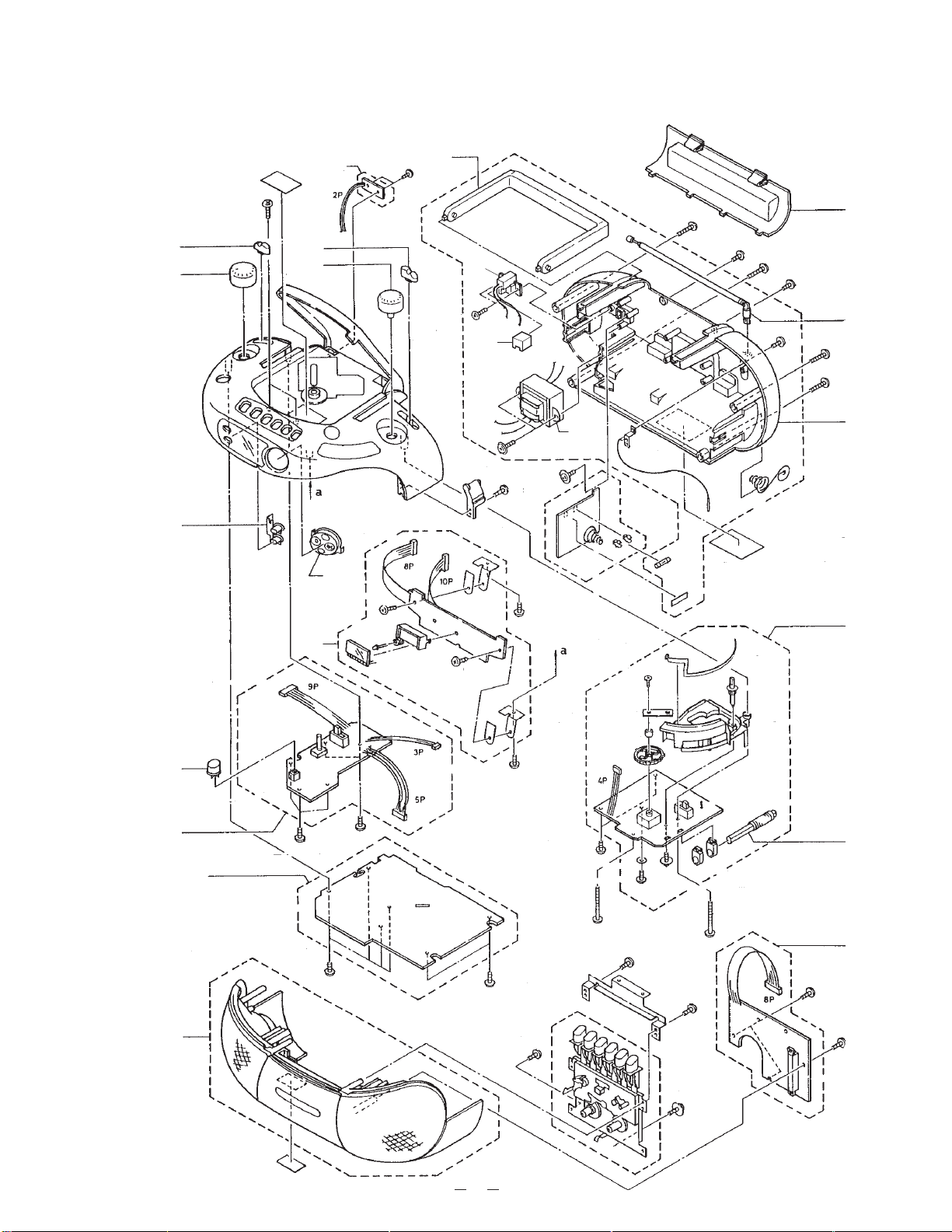
Cabinet
1 (2/2)
EXPLODED VIEWS
18
9
12
11
15
12
10
7
6
4
J301
S-10
20
T001
17
19
5
8
3
1 (1/2)
14
L001
2
45
Page 49

Cassette Mechanism
13-1
13-2
13-3
13-4
13-5
13-6
13
46
Page 50

Case Unit
14-7
15-8
14-8
14-4
14-2
14-6
14-3
14-7
14-5
14-1
47
Page 51

Top Case Unit
15-4
15-3
15-7
15-6
15-1
15-5
16
14-8
15-8
48
Page 52

AF0800181A
CASIO TECHNO CO.,L TD.
Overseas Service Division
8-11-10, Nishi-Shinjuku
Shinjuku-ku, Tokyo 160-0023, Japan
 Loading...