

Page 1
AP-10
(with price)
ELECTRONIC KEYBOARD
Page 2
CONTENTS
Safety Notice ......................................................................................2
Specifications.....................................................................................3
Block Diagram....................................................................................4
PCB Layout.........................................................................................5
Disassembly Instructions................................................................. 6
Circuit Description.......................................................................... 10
Major Waveforms .............................................................................12
Troubleshooting...............................................................................13
Wiring Diagram ................................................................................17
Exploded View..................................................................................18
Parts List...........................................................................................21
Schematic Diagrams....................................................................... 23
SAFETY NOTICE
CAUTION!
Danger of explosion if battery is incorrectly replaced.
Replace only with the same of equivalent type recommended
by the appliance manufacturer.Discard used batteries
according to manufacturer's instructions.
— 2 —
Page 3

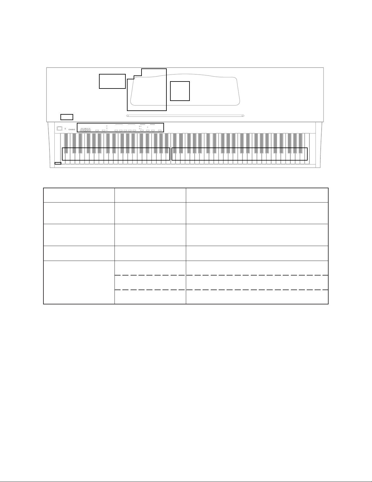
SPECIFICATIONS
GENERAL
Number of keys: 88
Polyphonic: 24-note
Preset tones: 5, Piano-1, Piano-2, Electric Piano, Pipe Organ, Strings
Layer: On/Off
Key transpose: Range of ± 1 octave by a semitone increment
Effects: Reverb-1/Reverb-2/Chorus reverb
Demo tunes: 5, 1. Grande valse brillante (F.F. Chopin)
2. One-Eighty (CASIO original)
3. Harmonious blacksmith (G.F. Handel)
4. Fugue in G minor (J.S. Bach)
5. Rainbow (CASIO original)
Memory: Number of songs: 2
System: Real-time recording
Memory capacity: Approx. 1200 notes total
Memory backup battery: Built-in lithium battery
Battery life: Approx. 5 years
Pedals: Damper, Soft/Sostenuto
Tuning control: 440Hz ± 50 cents
Built-In Speakers: 14 cm dia. 10 W input rating: 2 pcs.
MIDI: 8-channel, multi-timbral reception
Terminals: Line Out Jacks [Output impedance: 2 KΩ Output voltage: 1.5V (rms) MAX],
Phone Jacks, MIDI Jacks (IN, OUT)
Power source: 120V AC (for U.S.A.)
120V/220V/230V/240V (for other countries)
Power consumption: 35 W (with 120V AC), 30 W (with 220V/230V/ 240V AC)
Dimensions (HWD): Without stand:165 × 1340 × 480 mm (6-1/2 × 52-13/16 × 18-15/16 inches)
With stand: 805 × 1360 × 480 mm (31-11/16 × 53-9/16 × 18-15/16 inches)
Weight: Without stand:25.0 kg (55.1 lbs)/28.0 kg (61.7 lbs)
With stand: 35.5 kg (78.3 lbs)/38.5 kg (84.9 lbs)
Note: There are two models of AP-10, one has a keyboard cover, the other has no keyboard cover.
— 3 —
Page 4
Working Storage
RAM (64K-bit)
LSI304
LC3564SM-85
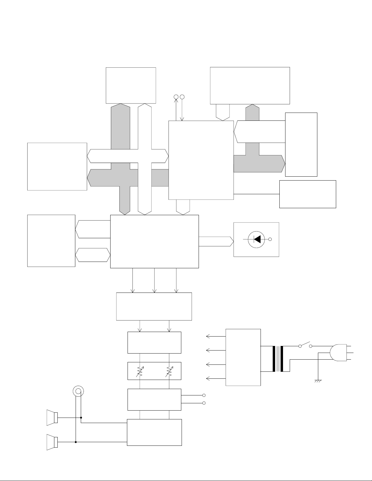
BLOCK DIAGRAM
MIDI
INOUT
Buttons
Sound Source ROM
(8M-bit)
LSI303
MX23C8100MC-
12CA27
Effect RAM
(256K-bit)
LSI305
LC333832M-70
EIO0 ~
EA0 ~
EA14
EIO7
MA0
~
MA12
MD0 ~ MD15
MA1 ~ MA19
MD0
~
MD7
UPD912GF-3BA
DSP
LSI302
HG51B227FB
LRCK SO BCK
CPU
LSI301
BCK, SO, LRCKMA0, MA1
HALL
STAGE
ROOM
SONGA
SONGB
MEMORY
KI0 ~ KI2
FI0 ~ FI10
SI0 ~ SI19
Keyboard
KC0 ~ KC7
Reset IC
IC 302
RN5VD24AA
LEDs
VDD
Speakers
Output
D/A Converter
LSI306
UPD6379GR
Filter
IC104
Main
Volume
Line Out Amp.
IC102
Power Amplifer
IC101
LA4620
LVDD
AVCC
AVDD
— 4 —
VDD
5V
5V
12.5V
5V
LINE OUT L
LINE OUT R
Voltage
Regulator
Q101 ~ 106,
and Q111
Power Switch
T101
Transformer
Page 5
PS3M
PCB LAYOUT
PS1M
MA1MPS2M
ON
OFF
POWER
PS4M
PCB
Main PCB
Sub PCB
Console PCB
Other PCBs
VOLUME
MIN MAX
CHORUS REVERB
REVERB2
PIANO E.PIANO
CN1M
REVERB1
TONE
HARPSICHORD
PIPE
ORGAN STRINGS
MEMORY
DEMO
SONG A
START/
STOP
SONG B
RECORD
TRANSPOSE/
DIGITAL
TUNE/MIDI
EFFECT
TP8-KY1M TP8-KY2M
JCM358-
MA1M
CPU, DSP, Sound Source ROM Working storage
RAM, Effect RAM Reset IC, DAC
PS2M
Filter, Lineout Amp., Power Amp. Power supply cir-
cuit. MIDI input/output.
CN1M
PS1
PS3M
PS4M
Main Volume, LEDs, Buttons
Fuse, Noise filter
Head phone Jack
Power lamp
AP-10
Components
— 5 —
Page 6
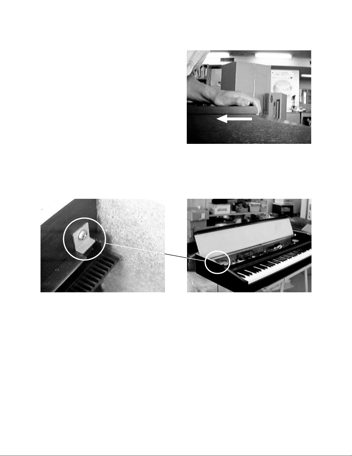
DISASSEMBLY INSTRUCTIONS
1. Disassembling top board
1-1. Remove 8 screws on the rear.
1-2. Slide the top board towards the rear.
The top board will be free from catches
on the case.
1-3. Lift the top board.
For keyboard-cover model
2. Disassembling the keyboard cover
2-1. Remove L-shape metal on inside of the side board.
2-2. Slide the keyboard cover to open fully.
2-3. Lift the keyboard cover.
For no-keyboard-cover model
2. Disassembling the front cover
2-1. Remove 4 screws at both ends of the front cover.
2-2. Remove the front cover.
— 6 —
Page 7

3. Disassembling the console panel
Note: To avoid scratch on the side board, put paper between the console panel and the side board at
both ends.
3-1. The console panel is fixed with screws and nuts.
Holding the nut, remove the screw.
3-2. Remove the screw fixing a grounding wire at the transformer.
3-3. Slide the console panel towards the front to free from catches.
3-4. Turn round the console panel.
3-5. Remove 2 screws fixing the power switch.
Insert paper here.
Hold this nut.
4. Disassembling keyboard unit
4-1. Remove 20 screws on the bottom.
4-2. Disconnect 2 connectors for the keyboard unit on the main PCB.
4-3. Remove the keyboard unit from the case.
Insert paper here.
— 7 —
Page 8
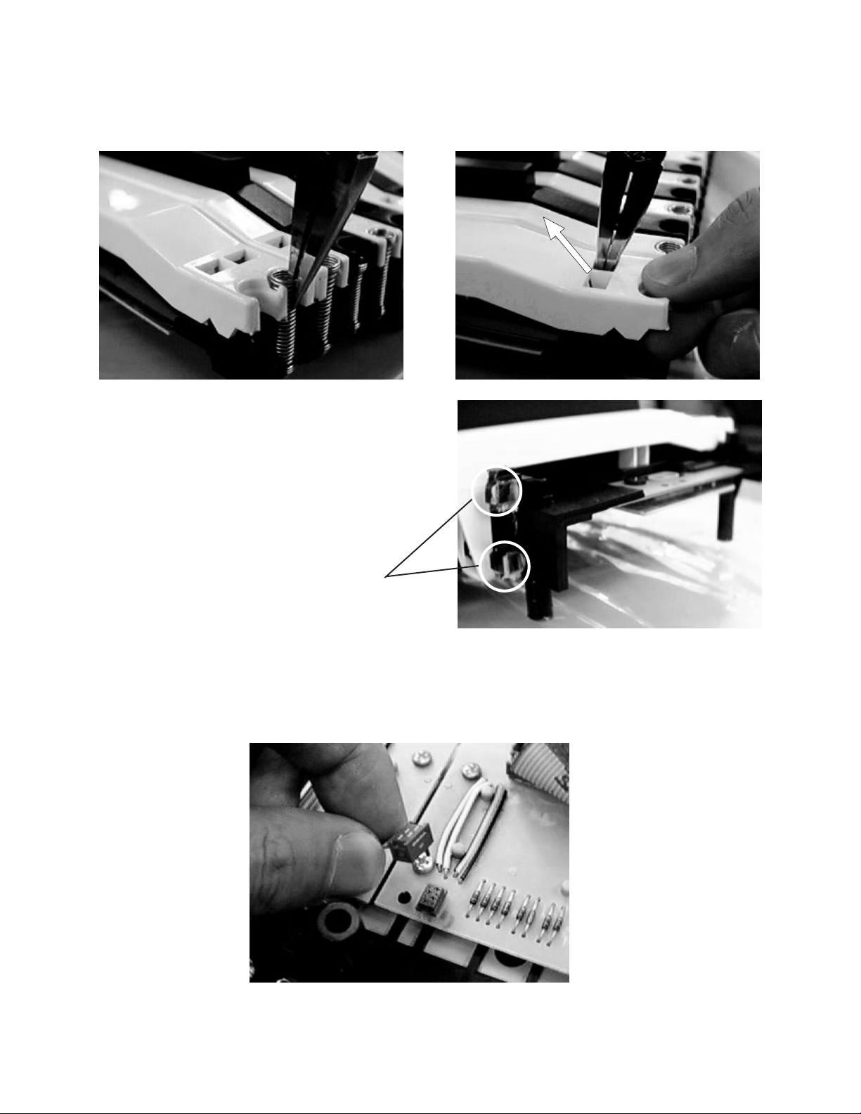
5. Disassembling keys
5-1. Remove a key spring.
5-2. Use a long-nose plier, pressing the hook, lift the key.
Apply grease G501
6. Disassembling keyboard PCBs
6-1. Turn around the keyboard unit to face the PCB up.
6-2. Disconnect the connector at middle of the keyboard.
6-3. Remove screws on keyboard PCBs
— 8 —
Page 9
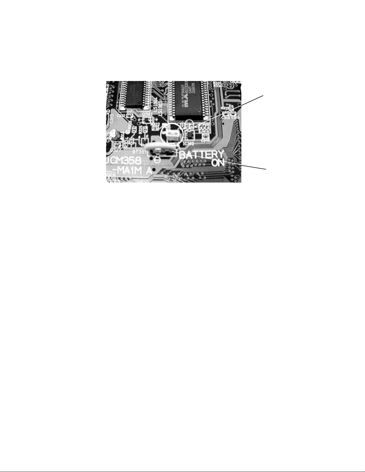
7. Replacing the main PCB
Note: The main PCB contains a lithium battery for memory back-up. Please remove the jumper before
replacing the PCB.
And make sure that the jumper is reset on new main PCB after replacing the PCB. Because no
jumper is set on a spare part of the main PCB.
Jumper and short-pin
Lithium battery
— 9 —
Page 10

KEYMATRIX
CIRCUIT DESCRIPTION
Second contact First contact
FI
KC
SI
KC0 KC1 KC2 KC3 KC4 KC5 KC6 KC7
FI0 A0 1 A0 # 1 B0 1 C1 1 C1 # 1 D1 1 D1 # 1 E1 1
SI0 A0 2 A0 # 2 B0 2 C1 2 C1 # 2 D1 2 D1 # 2 E1 2
EI1 F1 1 F1 # 1 G1 1 G1 # 1 A1 1 A1 # 1 B1 1 C2 1
SI1 F1 2 F1 # 2 G1 2 G1 # 2 A1 2 A1 # 2 B1 2 C2 2
FI2 C2 # 1 D2 1 D2 # 1 E2 1 F2 1 F2 # 1 G2 1 G2 # 1
SI2 C2 # 2 D2 2 D2 # 2 E2 2 F2 2 F2 # 2 G2 2 G2 # 2
FI3 A2 1 A2 # 1 B2 1 C3 1 C3 # 1 D3 1 D3 # 1 E3 1
SI3 A2 2 A2 # 2 B2 2 C3 2 C3 # 2 D3 2 D3 # 2 E3 2
FI4 F3 1 F3 # 1 G3 1 G3 # 1 A3 1 A3 # 1 B3 1 C4 1
SI4 F3 2 F3 # 2 G3 2 G3 # 2 A3 2 A3 # 2 B3 2 C4 2
LSI
UPD912GF-3BA
FI5 C4 # 1 D4 1 D4 # 1 E4 1 F4 1 F4 # 1 G4 1 G4 # 1
SI5 C4 # 2 D4 2 D4 # 2 E4 2 F4 2 F4 # 2 G4 2 G4 # 2
FI6 A4 1 A4 # 1 B4 1 C5 1 C5 # 1 D5 1 D5 # 1 E5 1
SI6 A4 2 A4 # 2 B4 2 C5 2 C5 # 2 D5 2 D5 # 2 E5 2
FI7 F5 1 F5 # 1 G5 1 G5 # 1 A5 1 A5 # 1 B5 1 C6 1
SI7 F5 2 F5 # 2 G5 2 G5 # 2 A5 2 A5 # 2 B5 2 C6 2
FI8 C6 # 1 D6 1 D6 # 1 E6 1 F6 1 F6 # 1 G6 1 G6 # 1
SI8 C6 # 2 D6 2 D6 # 2 E6 2 F6 2 F6 # 2 G6 2 G6 # 2
FI9 A6 1 A6 # 1 B6 1 C7 1 C7 # 1 D7 1 D7 # 1 E7 1
SI9 A6 2 A6 # 2 B6 2 C7 2 C7 # 2 D7 2 D7 # 2 E7 2
FI10 F7 1 F7 # 1 G7 1 G7 # 1 A7 1 A7 # 1 B7 1 C8 1
SI10 F7 2 F7 # 2 G7 2 G7 # 2 A7 2 A7 # 2 B7 2 C8 2
— 10 —
Page 11

POWER SUPPLY CIRCUIT
The power supply circuit generates five voltages as shown in the following table.
Name Voltage For operation of
VDD +5 V CPU, Reset IC, DSP, Sound source ROM, Working storage RAM, Effect RAM, LEDs
AVDD +5 V DAC
LVDD +5 V Power lamp
AVCC +12.5 V Filter
VC V Power amplifier
— 11 —
Page 12

MAJOR WAVEFORMS
A .5 s
1
2
3
CH1 5V CH2 5V
1 VDD CA connector pin 6
2 NMI CA connector pin 8
3 POWER CA connector pin 9
A 1ms
CH1
CH2
A 1ms
4
5
˜˜
CH1 .2V CH2 .2V
4 DAC output CA connector pin 1
5 DAC output CA connector pin 2
A 20µs
CH1
CH2
CH1
6
7
˜˜
CH1 .2V CH2 .2V
6 Filter output CF connector pin 5
7 Filter output CF connector pin 4
Tone : Pipe Organ
Key : A4
CH1
CH2
8
9
0
CH1 5V CH2 5V
CH3 5V
8 Key scan signal KC0 CC connector pin 2
9 Key scan signal KC1 CC connector pin 4
0 Key scan signal KC2 CC connector pin 6
CH2
CH3
— 12 —
Page 13

1. No power
TROUBLESHOOTING
Check fuse F101.
Is F101 blown up?
No
Check fuse F102.
Yes
Replace F101.
(A)
No
No
Is F102 blown up?
No
Measure output voltage of
transformer T101.
Is voltage 14 V AC?
Yes
Is voltage VC 17 V DC?
Yes
Is voltage VDD + 5 V DC?
Yes
Yes
Replace F102.
No
• Check power switch.
• Check position of voltage
selector.
Is it OK ?
No
Yes
Replace T101.
Replace PS2M PCB.
No
Yes
Does signal NMI vary
as Fig 1?
Yes
Does signal POWER vary
as Fig 1?
No
Replace MA1M PCB.
— 13 —
Set voltage selector at proper
positon.
Switch ON
VDD voltage
Signal NMl
0.9 sec
Signal POWER
Fig 1
Page 14

2. No sound
Press "Hall" button.
No
Yes
Does the LED light up?
Yes
Measure voltage at pin 9 of CA
connector.
Is the voltage +5 V?
Yes
Set main volume to maximum.
Touch pin1 of CA connector
with test rod (+) of multimeter
in resistance range, connecting
test rod (-) to ground.
Is a noise made?
No
Follow from (A) of "No sound"
troubleshooting.
Replace MA1M PCB.
No
Touch pin2 of CF connector
with test rod (+).
Is a noise made?
No
Replace PS2M PCB.
Yes
Check main volume and
connection to the volume.
— 14 —
Page 15

3. Distorted sound
Replace PS2M PCB.
Is a sound ok?
Replace MA1M PCB.
4. Certain keys do not function
Replace MA1M PCB.
Do the keys function?
Replace keyboard PCBs.
No
No
Yes
End
Yes
End
5. A certain key does not function
Clean the contact.
Does the key function?
Replace key contact rubber.
Does the key function?
Replace keyboard PCBs.
Yes
No
Yes
No
End
— 15 —
Page 16

6. A certain button does not function
Replace CN1M PCB.
Does the button function?
No
Replace MA1M PCB.
Yes
End
— 16 —
Page 17

WIRING DIAGRAM
POWER
Switch
POWER Lamp
CM-1
CM-2
JCM358-PS4M
JCM358-PS1 TRANSFORMER
BL
W
R
BK
BL
W
R
BK
TRANS
TRANSBRO
PEDAL
SOFT
N.C.
DAMPER
GND
UNIT
SOFT
DAMPER
GND
CE-1
CE-2
CE-3
CE-4
LVDD
DG
PHONES
CM-1
CM-2
MIDI
IN OUT
JCM358-PS3M
CG-1
CG-2
CG-3
CG-4
CG-5
CG-6
CG-7
DG
LVDD
L-OUT
L-IN
LHp
RHp
R-INAGR-OUT
CG-1
CG-2
CG-3
CG-4
CG-5
CG-6
CG-7
JCM358-PS2M
CA-1
CA-2
CA-3
CA-4
CA-5
CA-6
CA-7
CA-8
Rmel
LmelAGVDDFGVDDDGNMI
CA-1
CA-2
CA-3
CA-4
CA-5
CA-6
CA-7
CA-8
CG-8
CG-9
CG-8
CG-9
CA-9
CA-10
CA-11
POWER
M-IN
M-OUT
CA-9
CA-10
CA-11
LSP+
LSP–
RBKR
RSP+
RSP–
BK
CF-1
CF-2
CF-3
CF-4
CF-5
Lmel OUT
Rmel OUT
AG
Lmel IN
Rmel IN
Speakers
Left
Right
CF-R-O
CF-R-Y
CF-R-E
CF-R-BR
CF-R-R
JCM358-CN1M
CB-1
CB-2
CB-3
CB-4
CB-5
CB-6
CB-7
CB-8
SI0
KC0
FI0
KC1
SI1
KC2
FI1
KC3
123456789
TP8-KY1M
JCM358-MA1M
CB-9
CB-10
CB-11
CB-12
CB-13
CB-14
CB-15
CB-16
CB-17
CB-18
SI2
KC4
FI2
KC5
SI3
KC6
FI3
KC7
SI4
1011121314151617181920
CB-19
CB-20
FI4
CC-1
CC-2
CC-3
CC-4
CC-5
CC-6
CC-7
CC-8
SI5
KC0
FI5
KC1
SI6
KC2
FI6
KC3
123456789
TP8-KY2M
CC-9
CC-10
CC-11
CC-12
CC-13
CC-14
CC-15
CC-16
CC-17
CC-18
SI7
KC4
FI7
KC5
SI8
KC6
FI8
KC7
SI9
FI10
1011121314151617181920
CC-19
CC-20
FI9
SI10
CD-1
CD-2
CD-3
CD-4
CD-5
CD-6
CD-7
CD-8
CD-9
CD-10
CD-11
CD-12
CD-13
CD-14
HALL
STAGE
ROOM
VDD
SONGA
SONGB
MEMORY
KC0
KC1
KC2
KC3
KI2
KI1
KI0
CD-1
CD-2
CD-3
CD-4
CD-5
CD-6
CD-7
CD-8
CD-9
CD-10
CD-11
CD-12
CD-13
CD-14
— 17 —
Page 18

STAND
EXPLODED VIEW
V
R-8 R-9
R-10
x2
x4
x4
x1
x8
x2
R-11 R-11
U
x2
x4
— 18 —
Page 19

R-1
R-2
R-3
R-4
R-5
26
29
30
2
8
— 19 —
26
5
9
1
4
7
3
6
28
R-6
10
19
23
21
27
20
22
25
19
18
11
17
24
12 13 14 15 1618
Page 20

PARTS LIST
AP-10
Notes: This parts list does not include the cosmetic parts, which
parts are marked with item No. "R-X" in the exploded
view.
Contact our spare parts department if you need these
parts for refurbish.
1. Prices and specifications are subject to change without prior notice.
2. As for spare parts order and supply, refer to the
"GUIDEBOOK for Spare parts Supply", published
seperately.
3. The numbers in item column correspond to the same
numbers in drawing.
Page 21

FOB Japan
N Item Code No. Parts Name Specification Q M N.R.Yen R
Unit Price
Main PCB
BT301 3815 0714 Lithium battery CR1220/1VC 1 130 B
N D301 2390 2555 Chip schottky diode RB500V-40TE-17 1 24 B
IC302 2105 5173 MOS IC RN5VD42AA-TR 1 75 B
LSI301 2012 2072 LSI UPD912GF-3BA(T) 1 750 A
LSI302 2012 2079 LSI HG51B227FB-1
LSI303 2012 1890 LSI MX23C8100MC-12CA27
1 500 A
1 600 A
N LSI304 2012 1764 LSI LC3564SM-85-TRM 1 320 A
LSI305 2012 0777 LSI LC33832M-70-TLM 1 410 A
LSI306 2105 4746 LSI UPD6379GR-E1 1 150 A
Q301 2250 1162 Chip transistor 2SA1576A-T106R 1 8 B
Q302 2252 0637 Chip transistor 2SC4081-T106R 1 6 B
N
X301 2590 2387 Crystal oscillator HC-49/US24B 1 110 B
N X302 2590 2079 Ceramic oscillator CSACS16.00MX040-TC 1 68 B
N 1 6924 4790 Main PCB ass'y M358-MA1M M240318*1 1 5,590 A
Console PCB
LED401 - 406 2370 0630 LED LN282RPX-(TX3)
SW401 - 411
VR401 2765 0280
3412 0903 Tact switch EVQ-21405R
Slide volume
EWA-NAXCH1B14 1 100 A
621B
11 14 A
N 2 6924 4860 Console PCB ass'y M358-CN1M M240321*1 1 1,220 A
Amp. PCB
D101 2390 2366 Diode stack S4VB20-4033(L10) 1 190 B
N F102
3632 0427 Fuse, time-lag (S)T-6.3A
162A
F102 3632 0420 Fuse, time-lag UL-TSC-6.3A-N1 1 62 A
IC101 2114 1883 IC, Amp. LA4620 1 270 A
IC102, IC104 2114 1799 IC, OP-amp. M5218APR 2 35 B
IC103 2114 1421 IC, photocoupler PC900V 1 100 B
J101/102 3612 0789 Jack YKB21-5010 2 35 A
J103 3501 4816 DIN jack YKF51-5051 1 100 B
Q101 2253 0455 Transistor 2SD1762E,F 1 47 A
Q102 - 106, 2220 1387 Transistor 2SC1740SQ-TP-T
88A
Q109 - 111
Q107/108 2253 0420 Transistor 2SD1468SR,S-TP-T 2 16 A
ZD101 2360 2044 Zener diode MTZJ6.2AT-77-T 1 8 A
N ZD102 2360 2737 Zener diode MTZJ10CT-77-T 1 8 A
N ZD103 2360 2772 Zener diode MTZJ13CT-77-T 1 8 A
ZD104 - 106 2360 1946 Zener diode MTZJ5.6CT-77-T 3 8 A
N3
6924 8210 Amp. PCB ass'y M358-PS2M M140332*2
1 3,180 A
PS1 & PS3M PCBs
F101 3632 0287 Fuse, time-lag (S)T-0.63A 1 49 A
F101 3632 0294 Fuse, time-lag MT4-2A-N1 1 64 A
N 4 6924 4840 PCB ass'y M358-PS3M M340345*1 1 880 B
N 5 6924 4920 PCB ass'y M358-PS4M M340346*1 1 470 B
J104 3613 1533 Jack, phone HLJ4336-01-3040 1 170 A
Other electrical parts
LED101
6
N7
8
2320 9748 LED LN28RPH
3613 0217 Receptacle NC-174-10-C
3012 1449
Transformer
TE-358-1M1
6924 5260 Power button M340318-1
120B
1 110 C
1 1,290 B
113B
9 3412 1827 Power switch SDDLD1-A2-D 1 130 A
Keyboard unit
N 10 6924 1810 Keyboard unit 88TP/8CASIO 1 7,180 B
N 11 ~ 17 6924 9040 White key, 1-octave 88TP8(42123530) 7 450 A
N 20 6924 9030 Black key, 1-octave 88TP8(42123460) 7 360 A
Notes: N – New parts
M – Minimum order/supply quantity
R – Rank
— 21 —
Page 22

FOB Japan
N Item Code No. Parts Name Specification Q M N.R.Yen R
Unit Price
N 21 6924 9050 Spring, for key 88TP8(23105360) 88 21 B
N 22 6924 9190 Contact, rubber, for key, 12 88TP10/8(2564230) 6 150 A
N 23 6924 9200 Contact, rubber, for key, 13 88TP10/8(2564240) 1 160 A
N 24 6924 9060 Keyboard PCB (DX) 88TP10/8(42912070) 1 2,800 C
N 25 6924 9070 Keyboard PCB (SX) 88TP10/8(42912080) 1 3,500 C
Mechnical parts
26 3831 0966 Speaker SG13G01BFA
27 6924 5390 Rack L 1037153000
28 6924 5410 Rack R 1037154009
29 6919 3241 Slide knob M311405A-1
N 30 6924 5240 Button set 358 M240303*1
Stand
31
N 32 6924 7100 Screw set for AP-10's stand A190007300 1 410 B
6924 6670 Pedal box ass'y A190007200
AC cord
3701 0196 AC cord (120V, USA) UC-964-J01
3701 0595 AC cord (230V, Europe) EC-654-E06
3701 0588 AC cord (230V, UK) BC-323-J01
3701 0553 AC cord (240V, Australia) SC-101-J02 1 660 C
2 510 B
1 170 B
1 170 B
117B
1 110 B
1 3,920 B
1 650 C
1 720 C
1 860 C
Notes: N – New parts
M – Minimum order/supply quantity
R – Rank
— 22 —
Page 23

MAIN PCB (A) JCM358-MA1M
1
D/A Converter
5
4
DSP
SCHEMATIC DIAGRAMS
3
2
Sound
Source
Working
Storage
RAM
ROM
CPU
Effect RAM
— 23 —
10
8
9
Reset IC
Page 24

MAIN (B) & POWER SUPPLY PCBs JCM358-PS1/PS2M/PS3M/PS4M
1
3
2
45
6
7
Power Amp.
Page 25

CONSOLE PCB JCM358-CN1M
CHORUS
REVERB
REVERB2
REVERB1
DIGITAL EFFECT
— 25 —
Page 26

KEYBOARD PCB TP8-KY1
— 26 —
Page 27

KEYBOARD PCB TP-KY2
— 27 —
Page 28

MA0100661A
8-11-10, Nishi-Shinjuku
Shinjuku-ku, Tokyo 160, Japan
Telephone: 03-3347-4926
 Loading...