


 Loading...
SERVICE MANUAL
(with price
ELECTRONIC CASH REGISTER
110CR/PCR250 (EX-266)
150CR (EX-267)
JAN. 1995
Printer Model : M42V
INDEX
-
CONTENTS |
|
|
Page |
1.FEATURES ................................................................................... |
1 |
2.SPECIFICATIONS ................................................................................... |
1 |
3.OPTION ................................................................................... |
2 |
4.MAC OPERATION ................................................................................... |
2 |
5.BLOCK DIAGRAM ................................................................................... |
3 |
6.CIRCUIT EXPLANATIONS ............................................................................. |
4 |
6-1. Power supply circuit ................................................................................. |
4 |
6-2. Reset circuit ................................................................................... |
5 |
6-3. Data communication between CPU and EEPROM ................................. |
6 |
6-4. Printer drive circuit ................................................................................... |
8 |
6-5. Pin description ................................................................................... |
9 |
7.DISASSEMBLY ................................................................................. |
10 |
7-1. To open the upper case ......................................................................... |
10 |
7-2. To remove the Main PCB....................................................................... |
10 |
7-3. To remove the keyboard ass'y............................................................... |
10 |
8. DIAGNOSTOC OPERATIONS .................................................................... |
11 |
9. IC DATA ................................................................................. |
16 |
9-1. LB1268 ................................................................................. |
16 |
9-2. S-80728AN-Z ................................................................................. |
16 |
10.CIRCUIT DIAGRAM ................................................................................. |
17 |
11.PCB LAYOUT ................................................................................. |
28 |
12. PARTS LIST ................................................................................. |
29 |
1. FEATURES
Function |
110CR |
PCR-250 |
150CR |
150CR |
|
(U.S.A.,Canada) |
|||||
|
|
|
|
||
Depertment number |
4 |
8 |
4 |
8 |
|
|
|
|
|
|
|
PLU function |
Nil |
16 |
Nil |
16 |
|
|
|
|
|
|
|
Customer display |
Nil |
Nil |
Effective |
Effective |
|
|
|
|
|
|
|
PRG data back up function |
Effective |
Nil |
Effective |
Nil |
|
|
|
|
|
|
|
Calculator function |
Effective |
Effective |
Effective |
Effective |
|
|
|
|
|
|
2. SPECIFICATIONS
110CR/PCR-250
|
|
|
|
100V |
120V |
220V |
230/240V |
|
|
|
|
|
|
|
|
Power consumption |
In operation |
Max. |
4.5W |
0.08A |
0.09A |
0.04A |
0.05A |
|
|
|
|
|
|
|
|
|
|
Stand-by |
- |
0.05A |
0.06A |
0.03A |
0.04A |
|
|
|
|
|
|
|
|
|
Mode SW OFF |
|
- |
0.04A |
0.05A |
0.02A |
0.03A |
|
|
|
|
|
|
|
|
Memory protection |
Backup battery |
Mangan battery UM-3 x 3 pcs. (25°C) |
|
||||
|
|
|
|
|
|
|
|
|
Backup period |
1 year (25°C) |
|
|
|
|
|
|
|
|
|
|
|
|
|
|
Battery life |
Replace every 1 year |
|
|
|
||
|
|
|
|
|
|
|
|
Clock and calender |
Accuracy |
Within ±30 sec. per month |
|
|
|||
|
|
|
|
|
|
|
|
|
Auto calender |
Effective until 2099 A.D. |
|
|
|
||
|
|
|
|
|
|
|
|
Environment |
Operating temperature |
0°C ~ 40°C |
|
|
|
|
|
|
|
|
|
|
|
|
|
|
Operating humidity |
10% ~ 90% |
|
|
|
|
|
|
|
|
|
|
|
|
|
|
Storage temperature |
-25°C ~ 65°C |
|
|
|
|
|
|
|
|
|
|
|
|
|
|
Storage humidity |
10% ~ 95% |
|
|
|
|
|
|
|
|
|
|
|
|
|
Printer |
Model |
M-42V |
|
|
|
|
|
|
|
|
|
|
|
|
|
|
Print method |
Print wheel selecting type serial printer |
|
||||
|
|
|
|
|
|
|
|
|
Print digits |
12 digits (Amount 10 digits : Symbol 2 digits) |
|||||
|
|
|
|
|
|
|
|
|
MCBF |
700,000 lines |
|
|
|
|
|
|
|
|
|
|
|
|
|
Ink roller |
Model |
IR-40 (Purple) |
|
|
|
|
|
|
|
|
|
|
|
|
|
|
Life |
1,000,000 characters |
|
|
|
||
|
|
|
|
|
|
|
|
Roll paper |
Type |
Fine-quarity paper |
|
|
|
||
|
|
|
|
|
|
|
|
|
Size |
57.5±0.5 mm |
|
|
|
|
|
|
|
|
|
|
|
|
|
|
Roll diameter |
80 mm or less |
|
|
|
|
|
|
|
|
|
|
|
|
|
Drawer |
S drawer (Coin 5/Bill 4) |
DL-1313 ( for U.S.A.) |
|
|
|
||
|
|
|
|
|
|
|
|
|
S drawer (Coin 5/Bill 3) |
DL-1817 (for except U.S.A.) |
|
|
|||
|
|
|
|
|
|
|
|
|
M drawer (Coin 5/Bill 4) |
DL-2439 (for Europe, Other countries) |
|
||||
|
|
|
|
|
|
|
|
|
M drawer (Coin 8/Bill 4) |
DL-2749 (for Europe,U.K. and Other countries) |
|||||
|
|
|
|
|
|
|
|
- 1 -
150CR
|
|
|
120V |
220V |
230/240V |
Power consumption |
In operation |
Max. |
0.11A |
0.05A |
0.06A |
|
|
Stand-by |
0.07A |
0.04A |
0.05A |
|
Mode SW OFF |
|
0.06A |
0.03A |
0.04A |
Memory protection |
|
Same as 110CR |
|
|
|
Clock and calender |
|
Same as 110CR |
|
|
|
Environment |
|
Same as 110CR |
|
|
|
Printer |
|
Same as 110CR |
|
|
|
Ink roller |
|
Same as 110CR |
|
|
|
Roll paper |
|
Same as 110CR |
|
|
|
Drawer |
S drawer (Coin 5/ Bill 4) |
DL-1313 (for U.S.A.) |
|||
|
S drawer (Coin 5/Bill 3) |
DL-1817 (for Europe,U.K., |
|||
|
|
|
|
||
|
|
|
germany,Other countries) |
||
|
|
|
|
|
|
|
M drawer (Coin 5/Bill 4) |
DL-2439 (for Europe, |
|||
|
|
|
Canada, Other countries) |
||
|
M drawer (Coin 8/Bill 4) |
DL-2749 (for Europe,U.K., |
|||
|
|
|
Other countries) |
||
3. OPTIONS (110CR/PCR-250/150CR)
• Wet cover |
WT-69 |
4.MAC OPERATION (Memory All Clear operation)
1.Set the Mode Switch to OFF.
2.Plug the power cord of the ECR off an AC outlet.
3.Remove the memory protection batteries.
4.Leave the ECR a few minutes and plug the power cord into an AC outlet.
5.Set the memory protection batteries.
6.Turn the Mode Switch to REG position.
- 2 -
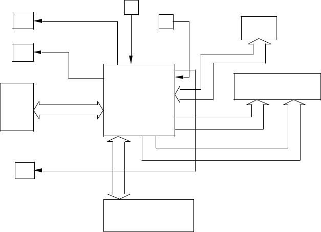
5. BLOCK DIAGRAM
Voltage detection
Buzzer
Winder Motor drive circuit
Printer drive circuit
Drawer drive circuit
Reset IC
EEPROM
DISPLAY |
CPU |
KEYBOARD
- 3 -
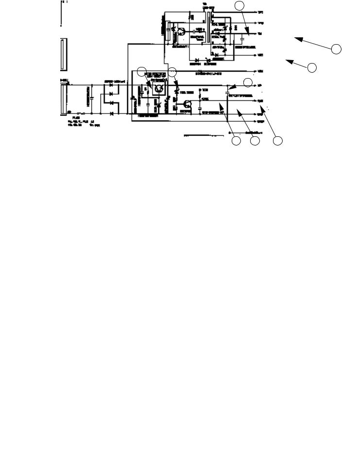
6. CIRCUIT EXPLANATION
6-1. Power supply circuit
G
I
A B H
 C
C
D E F
1.Plug the power cord into AC outlet, secondary voltage (9.65VAC) of the power transformer T1 will be appears at "A" point.
2.Then, its AC voltage is rectified by the diode bridge and change it to DC voltage.("B" point)
3.DC voltage appears more than 7V at the corrector of power transistor 2SD2396, and then the power transistor is turned on.
Then VP is supplied. ("C" point)
4.When the VP voltage becomes more than 3.3V, the transistor 2SD945 is turned on and then PWD signal becomes GND level. ("F" point)
When the PWD signal becomes GND level, CPU knows no power failure.
5.VP is supplied at the DC DC converter trans T2, the DC DC converter makes display and logic circuit voltage.
VN ,VF1,VF2 : Display voltage ("I", "J" point )
VDD : Logic circuit voltage ("H" point)
Transistor 2SD1803 is used for oscillating the primary voltage of DC DC converter trans.
- 4 -
|
D |
C |
|
|
|
|
|
G |
A |
|
I |
|
|
H
GND
B
E
|
|
|
|
|
|
|
F |
|
|
|
|
|
|
|
|
|
|
|
|
|
|
|
A |
B |
C |
D |
E |
F |
|
G |
H |
I |
Power ON |
9.65 VAC |
10.52V |
5.76V |
10.45V |
0.78V |
0.12V |
|
Pulse |
5.07V |
-23.9V |
Plug out |
0 |
0 |
0 |
0 |
0 |
4.13V |
|
0 |
4.30V |
0 |
Voltage level is measured at the following condition.
1.Plug the power cord in AC outlet.
2.Mode switch position : REG, display 0.00
3.Put in the memory protection batteries.
4.Plug out : Plug out the power cord , the memory protection batteries in.
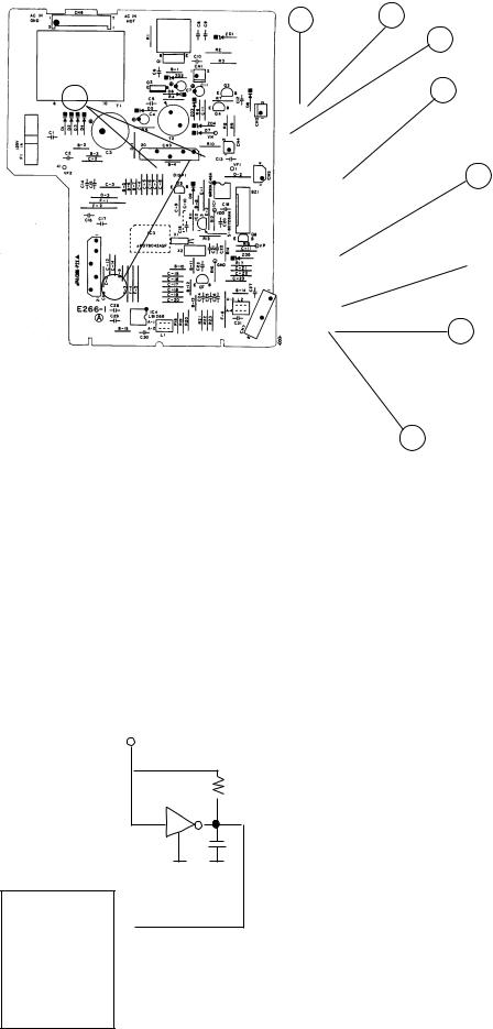
6-2. Reset circuit |
VDD |
|
S-80728AN 
GND
RESET 
Pin No.17
When the voltage level at the pin no.17 of CPU is not stable, CPU does not work properly.
To make a stable voltage, the reset IC(S-80728AN) is used for this circuit.
In case the voltage level of VDD becomes down output terminof reset IC is out the stable voltage.
- 5 -

6-3. Data communication between CPU and EEPROM
CPU |
EEPROM |
|
||||
|
1 |
|
|
|||
Pin No.23 |
CS |
|
||||
|
|
|
|
|||
2 |
CS : Chip enable |
|||||
|
SK |
|||||
Pin No.14 |
|
|
|
|||
|
|
|
SK : Sirial data clock |
|||
3 |
||||||
|
BR93LC46A |
|||||
|
DI : Serial data input |
|||||
Pin No.15 |
|
|
|
DI |
||
4 |
DO : Serial data outpu |
|||||
|
|
|||||
|
DO |
|
||||
Pin No.16 |
|
|
|
|
||
|
|
|
|
|||
|
|
|
|
|
|
|
EEPROM is a memory to possible write/erase by electricity .
The BR93LC46A privides efficient nonvolatile read/write memory arranged as 64 registers of 16 bits each.
(64 words X 16 bits = 1024 bits)
[Block diagram]
CS |
|
|
Command code |
|
|
|
|
|
Power detection |
|
||||||
|
|
|
|
|
|
|
||||||||||
|
|
|
|
|
||||||||||||
SK |
|
|
|
controller |
|
|
|
|
|
|
|
|
|
|
|
|
|
|
|
Clock generator |
|
|
|
|
|
|
|
|
|
|
|
|
|
|
|
|
|
|
|
|
|
|
|
|
|
|
|
|
||
|
|
|
|
|
Write |
|
|
|
High voltage |
|||||||
|
|
|
|
|
|
|
|
|
|
|
||||||
|
|
|
|
|
|
|
|
|
|
|
||||||
|
|
|
|
|
|
|
|
protection |
|
|
genarator |
|||||
|
|
|
|
|
||||||||||||
DI |
|
|
|
|
|
|
|
|
|
|
|
|
|
|
|
|
|
|
|
|
|
|
|
|
|
|
|
|
|
|
|
|
|
|
|
|
|
|
|
|
|
|
|
|
|
|
|
|
|
|
|
|
|
|
|
|
|
|
|
|
|
|
|
|
Command |
|
|
|
|
|
Address |
|
|
|
|
Address |
|
|
|
|
|
|
|
|
|||||
|
|
|
|
|
|
|
|
|
|
|
|
|
|
|
|
|
|
|
|
||||||||||
|
|
|
|
|
|
|
|
|
|
6 bits |
|
|
|
|
|
|
|
|
|||||||||||
|
|
|
|
|
|
|
|
|
|
|
|
|
|
|
|
|
|
|
|||||||||||
|
|
|
|
|
|
register |
|
|
|
|
|
buffer |
|
|
|
|
decorder |
|
|
|
|
|
|
|
|
||||
|
|
|
|
|
|
|
|
|
|
|
|
|
|
|
|
6 bits |
1024 bit |
||||||||||||
|
|
|
|
|
|
|
|
|
|
|
|
|
|
|
|
|
|
|
|
|
|
|
|||||||
|
|
|
|
|
|
|
|
|
|
|
|
|
|
|
|
|
|
|
|
|
|
|
|
|
|
|
|
|
|
|
|
|
|
|
|
|
|
|
|
|
|
|
|
|
|
|
|
|
|
|
|
|
|
|
|
|
|
|
|
|
|
|
|
|
|
|
|
|
|
|
|
|
|
|
|
|
|
|
|
|
|
||||||||
|
|
|
|
|
|
|
|
|
|
|
|
|
|
|
|
|
|
|
|
|
|
|
|
|
|
|
|
|
|
|
|
|
|
|
|
|
|
|
|
|
|
|
|
|
|
|
|
|
|
|
|
|
|
|
|
|
|
|
EEPROM array |
|
|
|
|
|
|
|
|
|
|
|
|
|
|
Data |
|
|
|
|
R/W |
|
|
|
|
|
|
|
|
||
|
|
|
|
|
|
|
|
|
|
|
|
|
|
|
|
|
|
|
|
|
|
|
|
|
|
||||
|
|
|
|
|
|
|
|
|
|
|
|
|
|
|
16 bits |
|
|
|
|
|
|
|
|
|
|
||||
DO |
|
|
|
Dammy bit |
|
|
|
|
|
|
register |
|
|
amplifier |
|
|
16 bits |
|
|||||||||||
|
|
|
|
|
|
|
|
|
|
|
|
|
|
|
|
||||||||||||||
|
|
|
|
|
|
|
|
|
|
|
|
|
|
|
|
|
|
|
|
|
|
|
|
|
|
|
|
|
|
|
|
|
|
|
|
|
|
|
|
|
|
|
|
|
|
|
|
|
|
|
|
|
|
|
|
|
|
|
|
|
|
|
|
|
|
|
|
|
|
|
|
|
|
|
|
|
|
|
|
|
|
|
|
|
|
|
|
|
|
- 6 -
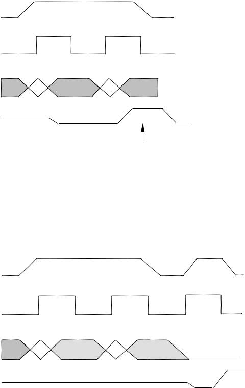
[Data reading procedure]
When the CPU read the dara of EEPROM, CPU send the CS signal and SK signal to EEPROM. Then, CPU send the address to EEPROM, and then EEPROM send the data to CPU.
CS
SK
DI |
Address |
DO |
Data |
|
|
|
Output data here |
[Data writing procedure]
When the CPU save the data to EEPROM, CPU sends the CS and SK signal to EEPROM. And CPU send the address and data to EEPROM from pin No.15.
When the EEPROM writes the data , EEPROM outputs the busy signal from DO terminal to CPU. After finish writing, EEPROM outputs the ready signal from DO terminal to CPU.
Status
CS
SK
Address |
Data |
DI
READY(H)
DO
High Impedance
BUSY(L)
- 7 -
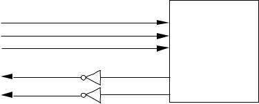
6-4. Printer drive circuit
|
RP |
M42 |
Pt |
PT |
|
Printer |
MD |
|
|
|
HD |
CPU
Pin No.44
Pin No.45
Pin No.47
Pin No.62
Pin No.63
When the CPU start printing, CPU send MD signal to rotate motor unit.
Then the printer send back the RP(reset pulse),PT and PT (Timing pulse) to CPU. After CPU receive RP,PT andPT, CPU knows the position of printin wheel.
And then, CPU send HD signal to operate the printing magnet when the character selected. The CPU counts the TP signal to select the character.
6-5. Pin description (CPU uPD78042AGF)
Pin No. |
Signal |
In/Out |
Mode SW |
Mode SW |
AC cord |
Description |
|
|
|
REG |
OFF |
Plug off |
|
1 |
P94/FIP6 |
Out |
Pulse |
-24V |
L |
Display digit signal DG7 |
2 |
P93/FIP5 |
Out |
Pulse |
-24V |
L |
Display digit signal DG6 |
3 |
P92/FIP4 |
Out |
Pulse |
-24V |
L |
Display digit signal DG5 |
4 |
P91/FIP3 |
Out |
Pulse |
-24V |
L |
Display digit signal DG4 |
5 |
P90/FIP2 |
Out |
Pulse |
-24V |
L |
Display digit signal DG3 |
6 |
P81/FIP1 |
Out |
Pulse |
-24V |
L |
Display digit signal DG2 |
7 |
P80/FIP0 |
Out |
Pulse |
-24V |
L |
Display digit signal DG1 |
8 |
VDD |
- |
+5V |
+5V |
+5V |
VDD terminal |
9 |
P27/SCK0 |
In/Out |
- |
- |
- |
Not used |
10 |
P26/SO0/SB1 |
In/Out |
- |
- |
- |
Not used |
11 |
P25/SI0/SB0 |
In/Out |
- |
- |
- |
Not used |
12 |
P24/BUSY |
In/Out |
- |
- |
- |
Not used |
13 |
P23/STB |
Out |
H |
H |
H |
Strobe signal for AVREF |
14 |
P22/SCK1 |
Out |
L |
H |
H |
SK signal for EEPROM |
15 |
P21/SO1 |
Out |
L |
H |
H |
DI signal for EEPROM |
16 |
P20/SI1 |
In |
H |
H |
H |
DO signal for EEPROM |
17 |
RESET |
In |
H |
H |
H |
Reset signal |
18 |
P74 |
Out |
H |
H |
L |
Drawer open signal |
19 |
P73 |
Out |
L |
H |
H |
Common signal for PAD condition |
20 |
AVSS |
- |
GND |
GND |
GND |
GND for AD converter |
21 |
P17/ANI7 |
In |
GND |
GND |
GND |
GND |
22 |
P16/ANI6 |
In |
GND |
GND |
GND |
GND |
23 |
P15/ANI5 |
Out |
L |
L |
H |
Chip enable signal for EEPROM |
24 |
P14/ANI4 |
In |
GND |
GND |
GND |
GND |
25 |
P13/ANI3 |
In |
GND |
GND |
GND |
GND |
26 |
P12/ANI2 |
In |
GND |
GND |
GND |
GND |
27 |
P11/ANI1 |
In |
GND |
GND |
GND |
GND |
28 |
P10/ANI0 |
In |
H |
H |
H |
Low battery detection terminal |
29 |
AVDD |
- |
H |
H |
H |
Power for AD converter |
30 |
AVREF |
In |
L |
L |
L |
Voltage for AD converter (VDD) |
31 |
XT1 |
In |
Pulse |
Pulse |
Pulse |
Sub system clock |
32 |
XT2 |
- |
Pulse |
Pulse |
Pulse |
Sub system clock |
33 |
VSS |
- |
GND |
GND |
GND |
GND |
34 |
X1 |
In |
Pulse |
L |
L |
Main system clock |
35 |
X2 |
- |
Pulse |
H |
H |
Main system clock |
36 |
P37 |
In |
L |
L |
L |
Mode switch position (OFF) |
37 |
P36/BUZ |
Out |
L |
L |
L |
Buzzer signal |
38 |
P35/PCL |
In |
L |
L |
L |
Mode switch position (Z) |
39 |
P34/T12 |
In |
L |
L |
L |
Mode switch position (X) |
40 |
P33/T11 |
In |
L |
L |
L |
Mode switch position (CAL) |
- 8 -
|
Pin No. |
Signal |
In/Out |
Mode SW |
Mode SW |
AC cord |
Description |
|
|
|
|
REG |
OFF |
Plug off |
|
|
41 |
P32/TO2 |
In |
H |
L |
L |
Mode switch position (REG) |
42 |
P31/TO1 |
In |
L |
L |
L |
Mode switch position (RF) |
|
43 |
P30/TO0 |
In |
L |
L |
L |
Mode switch position (PRG) |
|
44 |
P03/INTP3/CI0 |
In |
H |
L |
L |
Reset pulse RP from printer |
|
45 |
P02/INTP2 |
In |
H |
Pulse |
L |
Sub timimg pulse Pt from printer |
|
46 |
P01/INTP1 |
In |
L |
L |
H |
Power down signal PWD |
|
47 |
P00/INTP0/TI0 |
In |
H |
L |
L |
Main timing pulse PT from printer |
|
48 |
IC |
- |
GND |
GND |
GND |
GND |
|
49 |
P72 |
In |
H |
H |
H |
TAX PAD signal for Japan |
|
50 |
P71 |
In |
- |
- |
- |
PAD2 condition |
|
51 |
P70 |
In |
L |
H |
H |
PAD1 condition |
|
52 |
VDD |
- |
+5V |
+5V |
+5V |
Power (+5V) |
|
53 |
P127/FIP33 |
In |
L |
L |
L |
Key input signal KI7 |
|
54 |
P126/FIP32 |
In |
L |
L |
L |
Key input signal KI6 |
|
55 |
P125/FIP31 |
In |
L |
L |
L |
Key input signal KI5 |
|
56 |
P124/FIP30 |
In |
L |
L |
L |
Key input signal KI4 |
|
57 |
P123/FIP29 |
In |
L |
L |
L |
Key input signal KI3 |
|
58 |
P122/FIP28 |
In |
L |
L |
L |
Key input signal KI2 |
|
59 |
P121/FIP27 |
In |
L |
L |
L |
Key input signal KI1 |
|
60 |
P120/FIP26 |
In |
L |
L |
L |
Key input signal KI0 |
|
61 |
P117/FIP25 |
Out |
L |
L |
L |
Winder motor drive signal WMO |
|
62 |
P116/FIP24 |
Out |
L |
L |
L |
Printer moter drive signal PMO |
|
63 |
P115/FIP23 |
Out |
L |
L |
L |
Head drive signal for printer PHD |
|
64 |
P114/FIP22 |
Out |
Pulse |
L |
L |
Key common signal KC3 |
|
65 |
P113/FIP21 |
Out |
Pulse |
L |
L |
Key common signal KC2 |
|
66 |
P112/FIP20 |
Out |
Pulse |
L |
L |
Key common signal KC1 |
|
67 |
P111/FIP19 |
Out |
Pulse |
L |
L |
Key common signal KC0 |
|
68 |
P110/FIP18 |
Out |
H |
H |
H |
Not used (+5V) |
|
69 |
P107/FIP17 |
Out |
Pulse |
-24V |
L |
Display segment signal Sdp (Decimal point) |
|
70 |
P106/FIP16 |
Out |
Pulse |
-24V |
L |
Display segment signal Sg |
|
71 |
VLOAD |
- |
-24V |
-24V |
L |
Display voltage VN |
|
72 |
P105/FIP15 |
Out |
Pulse |
-24V |
L |
Display segment signal Sf |
|
73 |
P104/FIP14 |
Out |
Pulse |
-24V |
L |
Display segment signal Se |
|
74 |
P103/FIP13 |
Out |
Pulse |
-24V |
L |
Display segment signal Sd |
|
75 |
P102/FIP12 |
Out |
Pulse |
-24V |
L |
Display segment signal Sc |
|
76 |
P101/FIP11 |
Out |
Pulse |
-24V |
L |
Display segment signal Sb |
|
77 |
P100/FIP10 |
Out |
Pulse |
-24V |
L |
Display segment signal Sa |
|
78 |
P97/FIP9 |
Out |
H |
Pulse |
L |
Mode switch common signal |
|
79 |
P96/FIP8 |
Out |
Pulse |
-24V |
L |
Display digit signal DG9 |
|
80 |
P95/FIP7 |
Out |
Pulse |
-24V |
L |
Display digit signal DG8 |
|
Note : Above data is measured under following condition.
Mode SW REG : AC cord plug in the AC outlet, Memory protection batteries in, Mode SW position : REG
Mode SW OFF : AC cord plug in the AC outlet, Memory protection batteries in, Mode SW position : OFF
AC cord plug off : AC cord plug out the AC outlet, memory protection batteries in, Mode SW position : OFF
- 9 -
7. DISASSEMBLY
7-1. To open the upper case
1.Take out the printer cover and release the screw A.
2.Pushing the position B and slide the upper case to backward.
3.Lift up the upper case and remove the drawer connector.
Screw A
Slide this direction
Position B
Position B
7-2. To remove the Main PCB
1.Remove all cables on Main PCB and release 3 pcsof screw B.
2.Take out the Main PCB ass'y.
Screw B
Hook |
|
Hook |
|
|
|
Hook |
|
Hook |
|
7-3. To remove the keyboard ass'y
1. Release the 4 hooks and push the keyboard ass'y down.
- 10 -
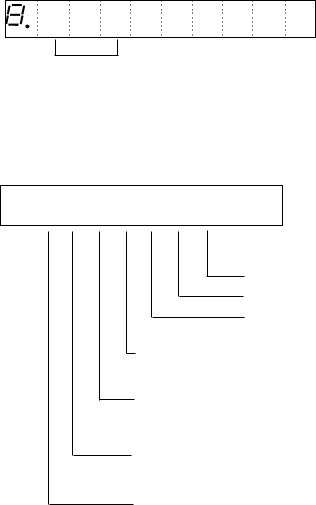
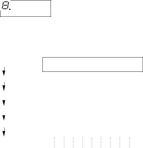
8. DIAGNOSTIC OPERATIONS
8-1. To start the diagnostic operation
1.Make MAC operation.
2.Turn the mode switch to PGM position.
3.Input "99999999" and press "SUB TOTAL" key.
Note : Do not issue the receipt under REG / RF / X / Z mode before execute the diagnostic. If the machine issued a receipt, the diagnostic does not start.
Print ing Layout |
|
Receipt sample |
|
|
|
0 0 - 0 0 - 0 0 |
|
0 0 - 0 0 - 0 0 |
0 0 - 0 0 # 0 0 0 2 |
|
0 0 - 0 0 # 0 0 0 2 |
- d1d2d3d4 - - d5d6d7 |
|
- 2 8 6 2 - - 1 - - |
|
|
|
d1d2d3d4 : Version No.
d5 : |
PAD condition |
||
|
0 : |
Japan |
|
|
1 : |
Export (ADD2) |
|
|
2 : |
US / Canada |
|
|
3 : |
Export (ADD3) |
|
d6 : |
4 : |
Export (ADD1) |
|
0 : |
Non taxable (Japan) |
||
|
|||
|
1 : |
Taxable (Japan) |
|
d7: |
- : |
Export version |
|
0 : |
118ER (Japan) |
||
|
|||
|
1 : |
108ER (Japan) |
|
|
- : |
Export version |
|
8-2. Check items
The following test can be checked in the test mode.
1.Key code check
2.Switch check
3.Individual function check
4.Country code write operation for EEPROM (PAD data)
- 11 -
8-3. Operations
1. Key code check (Hard key code)
When pressing a key, the machine displays the following key code.
Key code table
|
FEED |
029 |
|
027 |
|
|
021 |
|
|
|
|
|
|
|
|
|
|
|
C |
028 |
|
026 |
|
|
020 |
|
|
|
|
|
|
|
|
|
|
|
|
|
|
|
|
|
|
|
7 |
8 |
9 |
|
025 |
|
|
019 |
017 |
|
|
|
|
|
|
|
|
|
4 |
5 |
6 |
|
024 |
|
|
018 |
016 |
|
|
|
|
|
|
|
|
|
1 |
2 |
3 |
|
023 |
|
|
014 |
015 |
|
|
|
|
|
|
|
|
|
0 |
011 |
012 |
|
022 |
|
|
013 |
127 |
|
|
|
|
|
|
|
|
|
Display
0 2 2
022 : Hard key code
2. Switch check
Press " C " button, the switch condition is appered on a display.
 Always 0
No display
No display
PAD1 condition
EEPROM mounted : 1
PAD2 condition |
|
No EEPROM |
: 0 |
|
|
|
|
|
|
Open : 1 |
|
|
|
|
Short : 0 (Export version) |
|
|||
Non taxable PAD |
|
|
|
|
Short : 1 |
|
|
|
|
Open : 0 (export version) |
|
|||
FEED button |
|
|
|
|
OFF : |
0 |
|
|
|
ON : |
1 |
|
|
|
Mode key condition |
|
|
|
|
PRG : |
1 |
X : |
5 |
|
RF : |
2 |
Z : |
6 |
|
REG : |
3 |
OFF : |
8 |
|
CAL : |
4 |
Others: 0 |
|
|
- 12 -
3. Individual test
After finishing each test, the machine issues the following receipt.
Except US / Canada |
|
US / Canada |
|
|
|
#d1 |
|
d1 # |
|
|
|
Sample receipt |
d1 : Test command No. |
|
|
|
|
#1
1234567890ST#
1. General test
Press "1" key and "SUB TOTAL" key.
The machine executes the following tests.
All segment display
Set time and date
Date : 31st Dec. '94 Time : 23:59
Open drawer |
|
|
|
|
|
|
|
|
|
Print check |
|
|
|
|
|
|
Except US |
|
US |
|
|
|||
|
|
|||
|
|
|
|
|
Issue a test receipt |
1234567890ST# |
|
123456789012ST# |
|
|
|
|
||
Display test data
1 |
2 |
3 |
4 |
5 |
6 |
7 |
8 |
|
|
|
|
|
|
|
|
2. Mode selection (Receipt / Journal)
Press "2" key and "SUB TOTAL" key.
Change the mode to "Journal" from "Receipt".
3. Read/Write test for EEPROM (This test is effected at EEPROM version.)
Press "3" key and "SUB TOTAL" key.
Write a test data (1 word ) to test area of EEPROM and read it.
In case an error happens, the machine beep an error sound and issues an error receipt.
- 13 -
Loading...