

Page 1

R
LASER PRINTER
SERVICE MANUAL
MODEL:HL-1260
Page 2

No part this publication may be reproduced in any form or by any means without permission in writing
from the publisher.
Trademarks:
• BR-Script, and DX-1200 are registered trademarks of Brother Industries, Ltd.
• Centronics is a registered trademark of Genicom Corporation.
• PostScrip is a registered trademark of Adobe Systems Incorporated.
• IBM Proprinter XL is a registered trademark of International Business Machines Corporation.
• EPSON FX-850 is a registered trademark of Seiko Epson Corporation.
• HP-GL and HP Laser Jet 4 are registered trademarks of Hewlett Packard Company.
Page 3

PREFACE
This service manual contains basic information required for after-sales service of the laser printer
(hereinafter referred to as ”this machine” or ” the printer”). This information is vital to the service technician
in maintaining the high printing quality and performance of the printer.
This manual consists of the following chapters:
Chapter I : General
Features, specifications, etc.
Chapter II : Theory of Operation
Basic operation of the mechanical system and the electrical system, and their timing.
Chapter III : Electrical System
Theory of the electronics circuit
Chapter IV : Mechanical System
Requirements for a suitable location, disassembling and reassembling procedure of
mechanical system.
Chapter V : Maintenance and Servicing
Parts replacement schedule, list of tools, lubricants and cleaners.
Chapter VI : Troubleshooting
Reference values and adjustment, troubleshooting for image defects, troubleshooting
for malfunctions, etc.
Appendices : Engine Block Diagram, PCB Circuitry Diagrams, etc.
Information in this manual is subject to change due to improvement or re-design of the product. All relevant
information in such cases will be supplied in service information bulletins (Technical Information).
A thorough understanding of this printer, based on information in this service manual and service
information bulletins, is required for maintaining its quality performance and for fostering the practical ability
to find the cause of troubles.
Page 4

CONTENTS
CHAPTER I GENERAL
1. FEATURES ........................................................................................................................ I-1
2. SPECIFICATIONS.............................................................................................................. I-1
3. SAFETY INFORMATION.................................................................................................... I-6
3.1 Laser Safety (110 - 120V Model only)...................................................................... I-6
3.2 CDRH Regulations (110 - 120V Model only)............................................................ I-7
3.3 Additional Information .............................................................................................. I-7
4. PAR TS OF THE PRINTER................................................................................................. I-8
4.1 External Views ......................................................................................................... I-8
4.2 Cross Sectional View ............................................................................................... I-9
5. STORAGE AND HANDLING OF EP-ED CARTRIDGES.................................................. I-10
5.1 Storage of Sealed EP-ED Cartridges ..................................................................... I-10
5.2 Storage of Unsealed EP-ED Cartridges ................................................................. I-10
CHAPTER II THEORY OF OPERATION
1. BASIC OPERATIONS ....................................................................................................... II-1
1.1 Mechanical Configuration........................................................................................ II-1
1.2 Main Drive ............................................................................................................... II-2
1.3 Basic Sequence of Operations................................................................................ II-3
2. LASER/SCANNER SYSTEM ............................................................................................ II-4
3. IMAGE FORMATION SYSTEM......................................................................................... II-5
3.1 Outline..................................................................................................................... II-5
3.2 Printing Process ...................................................................................................... II-5
3.2.1 Electrostatic latent image formation stage ................................................ II-6
3.2.2 Developing stage ...................................................................................... II-8
3.2.3 Transfer stage ........................................................................................... II-9
3.2.4 Fixing stage ............................................................................................ II-10
3.2.5 Drum cleaning stage...............................................................................II-10
3.3 Operation ..............................................................................................................II-11
4. PAPER PICK-UP/FEED SYSTEM................................................................................... II-12
4.1 Outline...................................................................................................................II-12
4.2 Cassette Feed.......................................................................................................II-13
4.3 MP Tray Feed ........................................................................................................II-14
4.4 Paper Jam Detection.............................................................................................II-15
i
Page 5

CHAPTER III ELECTRICAL SYSTEM
1. MAIN PCB........................................................................................................................III-1
1.1 Outline.................................................................................................................... III-1
1.2 Video Controller Circuit ..........................................................................................III-2
1.3 Engine Controller Circuit ........................................................................................III-7
2. PAPER FEED DRIVE CIRCUIT ....................................................................................... III-9
3. DISPLAY CIRCUIT.........................................................................................................III-11
3.1 Outline..................................................................................................................III-11
3.2 Operation .............................................................................................................III-11
4. LOW-VOLTAGE POWER SUPPL Y ASSY.......................................................................III-12
4.1 Outline..................................................................................................................III-12
4.2 Protection Functions ............................................................................................III-12
5. HIGH-VOLTAGE POWER SUPPLY ASSY......................................................................III-14
5.1 Outline..................................................................................................................III-14
5.2 Operation of the Components of the High-Voltage Power Supply Assy ...............III-14
CHAPTER IV MECHANICAL SYSTEM
PRINTER DISASSEMBLING PROCEDURE
PRINTER BODY
1.1 Configuration.......................................................................................................... IV-3
1.2 Toner Cartridge Lid ................................................................................................IV-3
1.3 Side Cover L .......................................................................................................... IV-3
1.4 Font Cover Assy..................................................................................................... IV-4
1.5 Upper Cover Assy, Rear Cover Assy......................................................................IV-4
1.5.1 Upper cover assy, rear cover assy ...........................................................IV-4
1.5.2 Changeover guide, jam remove cover......................................................IV-5
1.6 Side Cover R.......................................................................................................... IV-5
1.7 DC Fan Motor......................................................................................................... IV-6
1.8 Main PCB ...............................................................................................................IV-6
1.9 Control Panel Unit .................................................................................................. IV-8
1.10 Scanner Unit .......................................................................................................... IV-9
1.11 Cartridge Stopper Assy .......................................................................................... IV-9
1.12 Paper Feed Chassis Unit .....................................................................................IV-10
1.13 Separation Pad Assy............................................................................................IV-11
1.14 MP PE Sub Actuator ............................................................................................ IV-12
1.15 P Feed /Size-SW PCB Assy................................................................................. IV-12
1.16 Side-Switch Spring ...............................................................................................IV-12
1.17 Regist Sensor Actuator ........................................................................................IV-13
1.18 MP Paper Detection Actuator...............................................................................IV-13
1.19 PE Sensor Actuator MP ....................................................................................... IV-13
1.20 Tray Sensor Holder .............................................................................................. IV-14
1.21 Roller Holder ........................................................................................................IV-14
1.22 Paper Pick-up Roller Assy, Bearing...................................................................... IV-15
1.23 Paper Pick-up Solenoid ........................................................................................IV-16
1.24 Paper Feed Motor Assy........................................................................................IV-16
1.25 MP Tray Cover......................................................................................................IV-17
1.26 MP Tray Assy ....................................................................................................... IV-17
1.27 Paper Path Separation Plate, Paper Path Separation Film .................................. IV-18
1.28 Latch .................................................................................................................... IV-19
1.29 Fixing Unit (for both 120V and 230V, the only difference is the halogen heater). IV-19
1.30 Transfer Unit......................................................................................................... IV-22
ii
Page 6

1.31 DC Gear Holder Assy........................................................................................... IV-23
1.32 PS Switch Wire, Remote Switch .......................................................................... IV-23
1.33 High-Voltage Power Supply PCB Assy................................................................. IV -24
1.34 Low-Voltage Power Supply PCB Assy.................................................................. IV-24
1.35 Toner Cartridge (EP-ED Cartridge)...................................................................... IV-25
1.36 Paper Tray ............................................................................................................ IV-25
CHAPTER V MAINTENANCE AND SERVICING
1. PERIODICAL REPLACEMENT PARTS ............................................................................ V-1
2. CONSUMABLE PARTS STANDARD ENDURANCE TABLE............................................. V-1
3. LIST OF STANDARD TOOLS............................................................................................ V-2
4. LIST OF LUBRICANTS AND CLEANERS ........................................................................ V-3
CHAPTER VI TROUBLESHOOTING
1. INTRODUCTION ..............................................................................................................VI-1
1.1 Initial Check............................................................................................................VI-1
1.2 Basic Procedure.....................................................................................................VI-2
2. TEST PRINTING AND MECHANICAL CHECK ...............................................................VI-2
2.1 Test Printing ...........................................................................................................VI-2
3. IMAGE DEFECTS ............................................................................................................VI-3
3.1 Image Defect Examples .........................................................................................VI-3
3.2 Troubleshooting Image Defects..............................................................................VI-4
4. TROUBLESHOOTING OF MALFUNCTIONS ................................................................ VI-11
5. TROUBLESHOOTING PAPER TRANSPORT PROBLEMS ...........................................VI-19
5.1 Paper Jams..........................................................................................................VI-19
5.2 Incomplete Paper Feed ........................................................................................VI-22
6. OPERATION ..................................................................................................................VI-23
6.1 Line Inspection Mode Procedure .........................................................................VI-23
6.2 DRAM Test ...........................................................................................................VI-25
7. STATUS MESSAGE LIST...............................................................................................VI-26
APPENDICES
1. Engine Block Diagram ....................................................................................................... A-1
2. Paper Feed/Size-SW PCB Circuitry Diagram (1/1)............................................................ A-2
3. Main PCB Circuitry Diagram (1/8) .....................................................................................A-3
4. Main PCB Circuitry Diagram (2/8) .....................................................................................A-4
5. Main PCB Circuitry Diagram (3/8) .....................................................................................A-5
6. Main PCB Circuitry Diagram (4/8) .....................................................................................A-6
7. Main PCB Circuitry Diagram (5/8) .....................................................................................A-7
8. Main PCB Circuitry Diagram (6/8) .....................................................................................A-8
9. Main PCB Circuitry Diagram (7/8) .....................................................................................A-9
10. Main PCB Circuitry Diagram (8/8) ................................................................................... A-10
11. Control Panel PCB Circuitry Diagram (1/1) ..................................................................... A-11
12. Scanner LD PCB Circuitry Diagram (1/1) ........................................................................ A-12
iii
Page 7

CHAPTER I GENERAL
1. FEATURES
A. This high-speed, non-impact (low-noise) printer is based on electrophotography, electronics
and laser technology.
B. The printer is compact and easy to carry. The internally-storable, front-loading paper
cassette enables you to save an occupation space for the machine; the printer can now
be installed in a smaller place.
C. The charging roller, developing cylinder, photosensitive drum and cleaner of the printer
are combined into a single assembly called an ”EP-ED cartridge”. The cartridge can be
replaced by the user when necessary without a need of service call. High printing quality
is maintained by a simple cleaning procedure.
D. Laser beam safety is designed into the printer. The printer is approved by the US Center
for Devices and Radiological Health (CDRH).
E. Paper can be fed in two ways, by the multi-purpose paper feed tray and paper cassette.
F. Maintenance is easy with print component units which are directly detachable, and they
require no adjustment after reassembly.
2. SPECIFICATIONS
(1) Type Desktop page printer
(2) Printing method Electrophotography (single-component dry toner)
(3) Printing speed
Cassette feed 12 pages/minute (A4/Letter size by cassette feed)
10.2 pages/minute (Legal size)
(4) First print time Approx. 20 seconds
(A4 size by face-down print delivery from the paper cassette)
(5) Warm-up (WAIT) time Max. 1 minute at 20°C (68°F)
(6) Optical system
Laser Semiconductor laser
Output power : 5mW max.
Wave length
Scanning system Rotating six-faced polygon mirror
(7) Resolution
Horizontal 600 dots/inch and high resolution control (HRC)
Vertical 600 raster lines/inch
: 780 nm
I - 1
Page 8

(8) Printing system
Photosensitive drum OPC
Charging Charging Roller
Exposure Laser scanning system
Development Toner projection development system
Paper feed Cassette or manual feed
Image transfer Roller method
Separation Natural(utilizing a small drum radius), Static charge eliminator
Fixing Heated fixing roller
Toner supply Included in the replaceable EP-ED cartridge
Life expectancy 6000 pages/cartridge
(9) Paper
Cassette feed Plain paper for Letter, Legal, A4, ISO B5, A5, ISO B6, A6,
Multi-purpose Tray Plain paper of 90 x 148 mm 216 x 356 mm (recommended:
(10) Cassette (Tray 1)
Executive (A4 or letter size paper with the print density set at
2
level 8 with 4% coverage, recommended: 60 g/m
105 g/m )
and Envelope (com10, monarch, C5, DL, ISO B5)
2
60g/m 135 g/m , overhead projector (OHP) film, postcards,
2
label stock and envelopes (specified sizes)
2
Universal cassette A4, Letter, Legal, ISO B5, Executive, A5, ISO B6, and A6
Maximum load height 55 mm (500 sheets of 80 g/m paper)
Feedable paper type 60 105 g/m
2
Envelopes 40 envelopes
(11) Print delivery Face-down or (face-up)
(12) Print delivery tray capacity
Face-down 250 sheets (80 g/m )
2
Face-up Discharge only
2
I - 2
Page 9
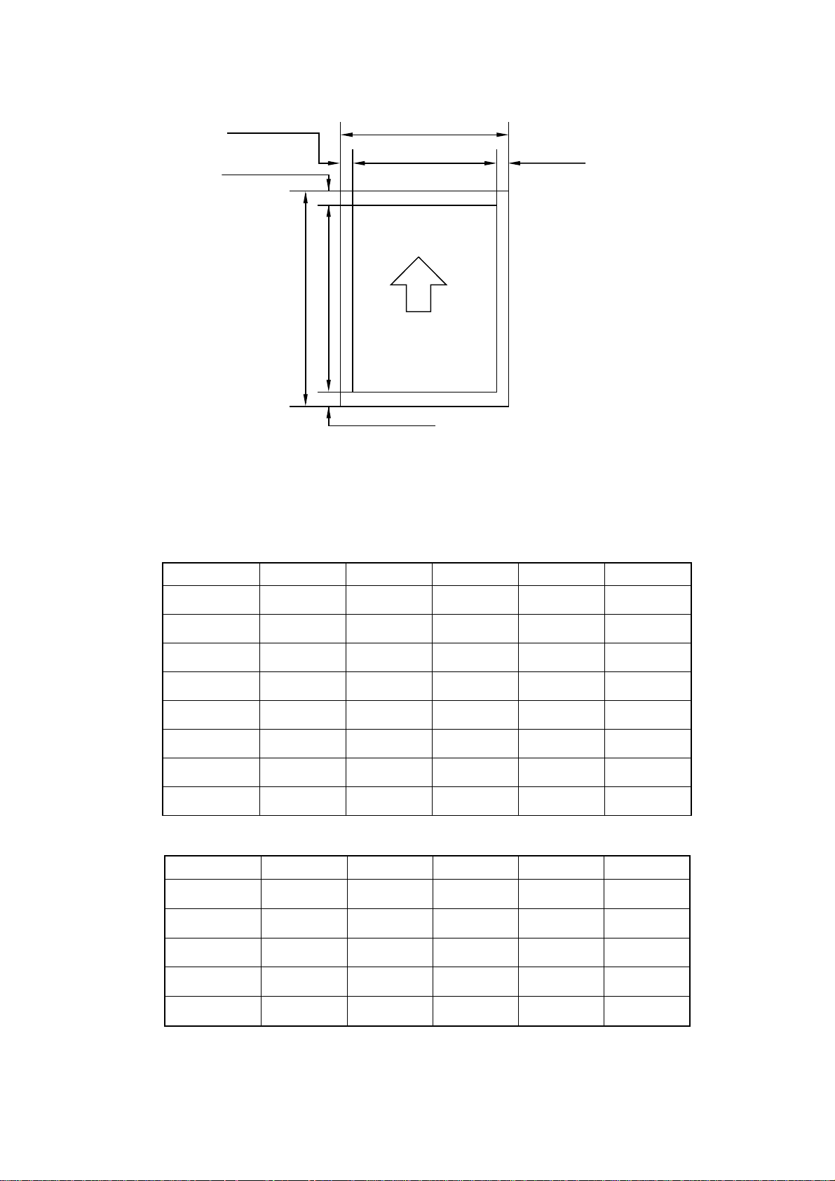
(13) Effective printing area
E
E
A
C
E
Printable area
D
B
E
Figure 1.1 Printable Area
Effective printable area is referred to as a area within which is guaranteed the printing of all
interface signal data on a hard copy without any omission.
The tables below shows the effective printable area for each paper size.
Table 1.1 Plain Paper
SIZE A (mm) B (mm) C (mm) D (mm)
A 4
Letter
Legal
B 5 (ISO)
Executive
A 5
B 6 (ISO)
A 6
210.0 297.0 203.2
215.9 279.4 207.4 270.9
215.9 355.6 207.4 347.1
176.0 250.0 167.5 241.5
184.2 266.7 175.7 258.2
148.0 210.0 139.5 201.5
125.0 176.0 116.5 167.5
105.0 148.0 96.5 139.5
Table 1.2 Envelope
SIZE A (mm) B (mm) C (mm) D (mm)
COM-10
MONARCH
DL
104.8 241.3 96.3
98.4 190.5 89.9 182.0
110.1 221.0 101.6 212.5
288.5
232.8
E (mm)
3.39 ± 1.0
4.23 ± 1.0
4.23 ± 1.0
4.23 ± 1.0
4.23 ± 1.0
4.23 ± 1.0
4.23 ± 1.0
4.23 ± 1.0
E (mm)
4.23 ± 1.0
4.23 ± 1.0
4.23 ± 1.0
C5
B5 (ISO)
162.2 228.6 154.1 220.1
176.0 250.0 167.5 241.5
(The sizes above are nominal sizes according to ISO.)
An A4 sheet accepts 80 PICA-pitch characters (203.2mm).
I - 3
4.23 ± 1.0
4.23 ± 1.0
Page 10

(14) Standard interfaces Automatic interface selection
• Centronics, Bi-directional parallel
• RS-232C serial
Baud rate : 150, 300,1200, 2400, 4800, 9600
19200, 38400, 57600 bps
Stop bit : 1 bit
Start bit : 1 bit or 2 bits
Data length : 7 bits or 8 bits
Parity : Odd, Even, or None
Protocol : Xon/Xoff or DTR
(15) Emulation Automatic emulation selection
• HP Laser Jet 4 (PCL Level 5
• EPSON FX-850
• IBM Proprinter XL
• BR-Script level 2 (PostScript language emulation interpreter)
• HP- GL
e
)
(16) CPU 79R3041 (20MH
Z)
(17) Resident fonts 75 scalable fonts and 12 bitmapped fonts
HP Laser Jet 4, EPSON FX-850, IBM Proprinter XL
Scalable Fonts:
Intellifont Compatible Fonts:
• Albertville, Extrabold
• Antique Oakland, Oblique, Bold
• Brougham, Oblique, Bold,
Bold Oblique
• Cleveland Condensed
• Connecticut
• Guatemala Antique, Italic, Bold,
Bold Italic
• Letter Gothic, Oblique, Bold
• Maryland
• Oklahoma, Oblique, Bold,
Bold Oblique
Windows 3.1 Compatible Fonts:
• Tennessee Roman, Italic, Bold,
Bold Italic
• Helsinki, Oblique, Bold, Bold Oblique
• BR Symbol
• W Dingbats
BR-Script Fonts:
• Atlanta Book, Book Oblique, Demi,
Demi Oblique
• Copenhagen Roman, Italic, Bold,
Bold Italic
• Portugal Roman, Italic, Bold, Bold Italic
• Calgary Medium Italic
• PC Brussels Light, Light Italic, Demi,
Demi Italic
• PC Tennessee Roman, Italic, Bold,
Bold Italic
• Utah, Oblique, Bold, Bold Oblique
• Utah Condensed, Oblique, Bold,
Brother Original Fonts:
• Bermuda Script
• Germany
• San Diego
• US Roman
Bold Oblique
Bitmapped Fonts (Portrait and Landscape):
• Letter Gothic 16.66 Medium, Italic, Bold, Bold Italic
• OCR-A
• OCR-B
I - 4
Page 11

BR-Script Level 2 Mode
Scalable Fonts:
• Atlanta Book, Book Oblique, Demi,
Demi Oblique
• Brussels Light, Light Italic, Demi,
Demi Italic
• Brougham, Oblique, Bold, Bold Oblique
• Helsinki, Oblique, Bold, Bold Oblique
• Helsinki Narrow, Oblique, Bold,
Bold Oblique
• Copenhagen Roman, Italic, Bold,
Bold Italic
• Portugal Roman, Italic, Bold, Bold Italic
• Tennessee Roman, Italic, Bold, Bold Italic
• Calgary Medium Italic
• BR Symbol
• BR Dingbats
• Albertville, Extrabold
• Antique Oakland, Oblique, Bold
• Cleveland Condensed
• Conecticut
• Guatemala Antique, Italic, Bold, Bold Italic
• Letter Gothic, Oblique, Bold
• Maryland
• Oklahoma, Oblique, Bold, Bold Oblique
• Utah, Oblique, Bold, Bold Oblique
• Utah Condensed, Oblique, Bold,
Bold Oblique
• Bermuda Script
• Germany
• San Diego
• US Roman
(18) RAM 2M bytes (expandable to 26M bytes)
(19) Font cartridge/card slots Two slots
One font cartridge slot and one font card slot
(20) Power souse USA and Canada : AC 110 to 120 V, 60 H
Europe and Australia : AC 220 to 240 V, 50 HZ
(21) Power consumption Printing : 500 WH or less
Stand-by : 80 WH or less
Sleep : 20 WH
(22) Noise Printing : 49 dB A or less
Stand-by : 40 dB A or less
(23) Dimensions (W x H x D) 371.6 x 326.5 x 393 mm (14.6 x12.9 x 15.5 inches)
(24) Weight Approx. 15 kg (32.6 Ibs)
(25) Environmental conditions
Operating Temperature 10 ~ 32.5°C
environment Relative humidity 20 ~ 80%RH
(No condensation allowed)
Air pressure 613 ~ 1013 hPa
(0 ~ 2,500 m above sea level)
Non-operating Temperature 0 ~ 35°C
environment Relative humidity 10 ~ 80%RH
(No condensation allowed)
Storage conditions
Z
• Printer Temperature
Normal (total storage time x 9/10)
0 ~ 35°C
Severe (total storage time x 1/10)
High Low
35°C ~ 60°C -20°C ~ 0°C
Temperature change (within 3 minutes)
High Low
60°C 15°C -20°C 25°C
I - 5
Page 12

Relative humidity
Normal (total storage time x 9/10)
35 ~ 85%RH
Severe (total storage time x 1/10)
High Low
85 ~ 95%RH 10 ~ 35%RH
Air pressure 613 ~ 1013 hPa
Total storage time 0.5 years
• EP-ED cartridge Temperature
Normal (2.45 years max.)
0 ~ 35°C
Severe (0.05 years max.)
High Low
35°C ~ 40°C -20°C ~ 0°C
Temperature change (within 3 minutes)
High Low
40°C 15°C -20°C 25°C
Relative humidity
Normal (2.45 years max.)
35 ~ 85%RH
Severe (0.05 years max.)
High Low
85 ~ 95%RH 10 ~ 35%RH
Air pressure 613 ~ 1013 hPa
Maximum total storage time: 2.5 years including used time
3. SAFETY INFORMATION
3.1 Laser Safety (110 ~ 120V Model only)
This printer is certified as a Class 1 laser product under the US Department of Health and
Human Services (DHHS) Radiation Performance Standard according to the Radiation
Control for Health and Safety Act of 1968. This means that the printer does not produce
hazardous laser radiation,
Since radiation emitted inside the printer is completely confined within the protective
housings and external covers, the laser beam cannot escape from the machine during any
phase of user operation.
I - 6
Page 13

3.2 CDRH Regulations (110 ~ 120V Model only)
The center for Devices and Radiological Health (CDRH) of the US Food and Drug
Administration implemented regulations for laser products on August 2, 1976. These
regulations apply to laser products manufactured from August 1, 1976. Compliance is
mandatory for products marketed in the United States. The label shown below indicates
compliance with the CDRH regulations and must be attached to laser products marketed in
the United States.
MANUFACTURED :
BROTHER INDUSTRIES, LTD.
15-1, Naeshiro-cho, Mizuho-ku Nagoya 467, Japan.
This product complies with FDA radiation
performance standards , 21 CFR chapter 1
subchapter J.
Figure 1.2
Caution: Use of controls, adjustments or performance of procedures other than those
specified in this manual may result in hazardous radiation exposure.
3.3 Additional Information
When servicing or adjusting the optical system of the printer, be careful not to place
screwdrivers or other reflective objects in the path of the laser beam. Be sure to take off any
personal accessories such as watches and rings before working on the printer. A reflected
beam, though invisible, can permanently damage the eyes.
Since the beam is invisible, the following label is attached to the inside of covers where
danger of exposure to laser radiation exist.
Figure 1.3
I - 7
Page 14
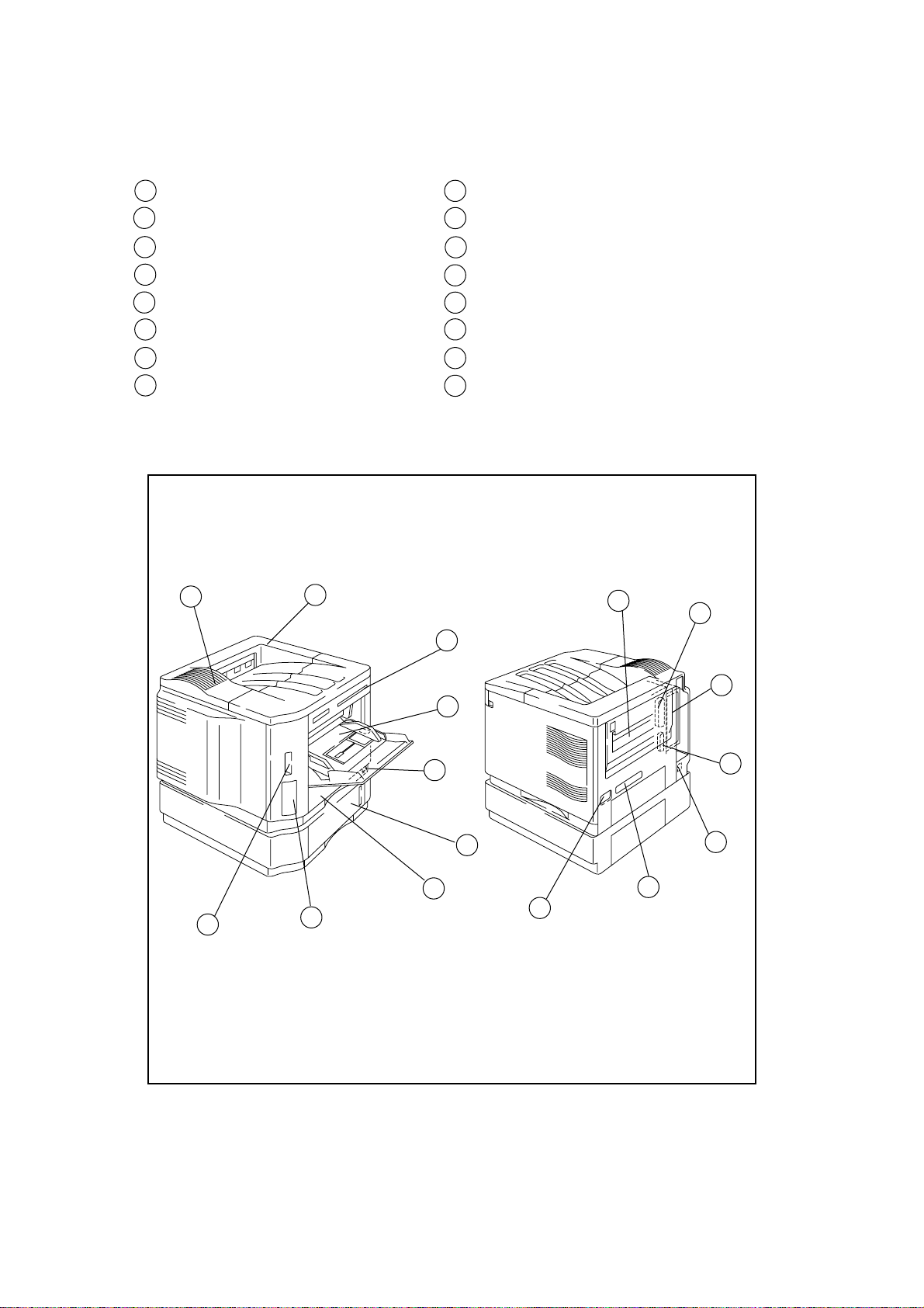
4. PARTS OF THE PRINTER
4.1 External Views
1 Upper cover
2 Control panel
3 MP tray
4 Tray 1
5 Tray 2 (Option)
6 Font card slot
7 Font cartridge slot
8 Power switch
11
9 AC inlet
10 Face-up print delivery port
11 Fan outlet port
12 Rating label
13 Optional I/O slot
14 RS-232C interface connector
15 Centronics interface connector
16 Optional interface connector
1
2
10
15
13
3
8
5
4
6
7
Figure 1.4
9
12
14
16
I - 8
Page 15
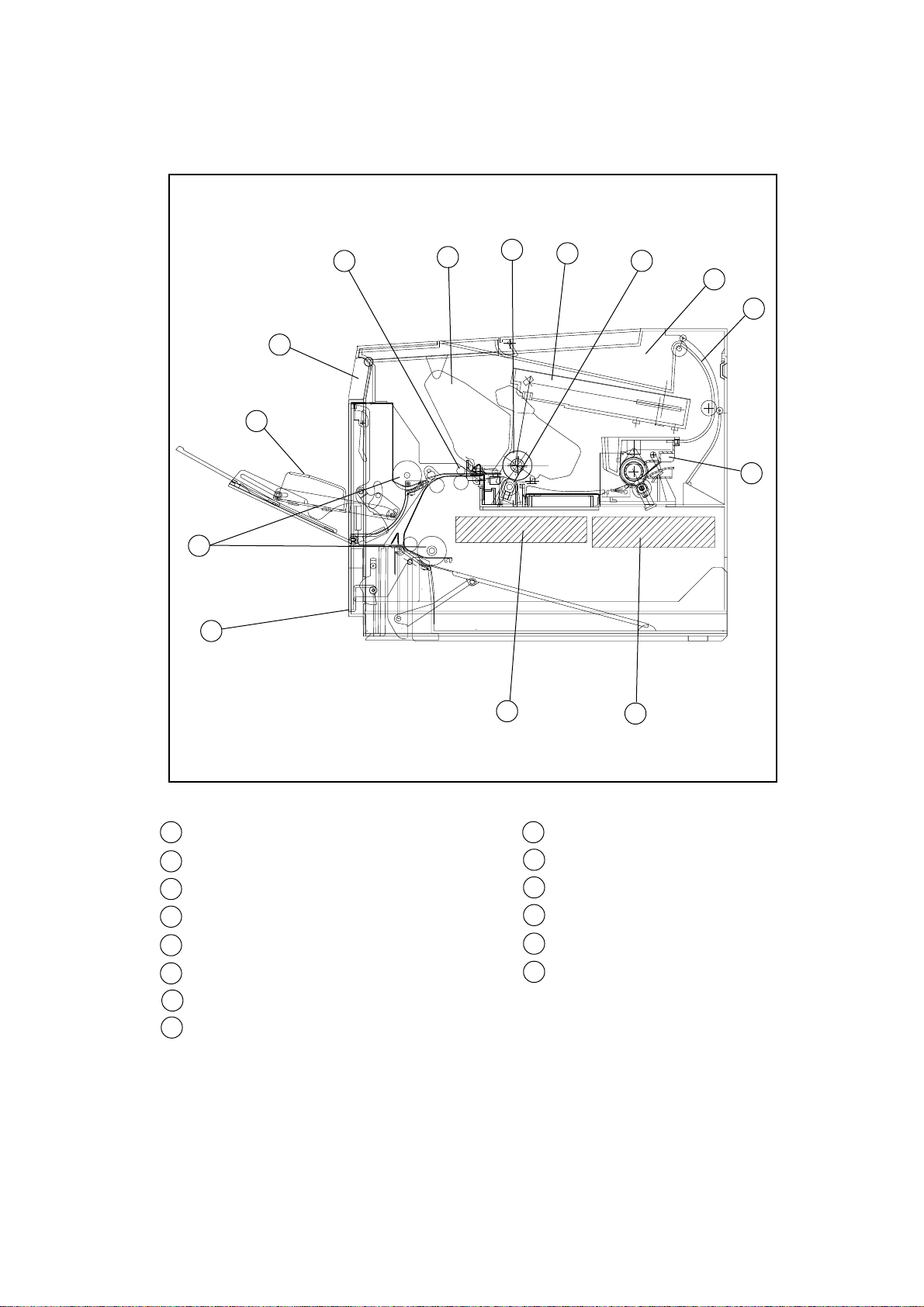
4.2 Cross Sectional View
12
11
13
14
1
2
3
4
5
6
7
8
1 Registration rollers
2 EP-ED cartridge
3 Photosensitive drum
4 Laser scanner unit
5 Transfer unit
6 Face-down tray
7 Print-delivery path
8 Fixing unit
10
Figure 1.5
9
9 Low-voltage power supply assy
10 High-voltage power supply assy
11 Paper cassette (Tray 1)
12 Pick-up rollers
13 MP tray
14 Control panel
I - 9
Page 16

5. STORAGE AND HANDLING OF EP-ED CARTRIDGES
An EP-ED cartridge is influenced by the storage conditions even if it is sealed in its package,
so its life depends on the way in which it is used or stored. EP-ED cartridges should be
handled carefully.
5.1 Storage of Sealed EP-ED Cartridges
When storing sealed EP-ED cartridges in a warehouse or workshop, the storage conditions
shown in (25) Environmental conditions on Page 1-5 must be met. Follow the instructions
below:
1) Avoid direct sunlight.
2) Do not store cartridges on a surface that is subject to vibration.
3) Do not hit or drop the packages containing cartridges.
4) The cartridges should be stored horizontal when they are removed from the body (with
their label side upside).
5) Avoid putting the cartridges near a CRT screen, a disk or a floppy disk (to keep their data
from being destroyed).
5.2 Storage of Unsealed EP-ED Cartridges
Each EP-ED cartridge contains a photosensitive drum that has an organic photoconductor
(OPC) which deteriorates when exposed to strong light. It also contains toner. The user,
therefore, should be fully informed about the correct storage and handling of EP-ED
cartridges.
(1) Storage requirements
1) Avoid places exposed to direct sunlight or near a window. Do not leave an EP-ED
cartridge in a car in warm or hot weather even if it is in its storage box.
2) Avoid places with a too-high or too-cool temperature and/or humidity. Also avoid
places exposed to sudden temperature or humidity changes (such as near an air
conditioner outlet).
3) Avoid dusty places or places exposed to ammonia fumes or other harmful fumes.
4) Do not store an EP-ED cartridge in a temperature above 40°C.
(2) EP-ED cartridge life
The effective life of an EP-ED cartridge is 2.5 years from the date of manufacture
(printed on the cartridge.) The expiry year and month (date of manufacture plus 2.5
years) is shown on the EP-ED cartridge box. An EP-ED cartridge used after the expiry
may produce low-quality printing, so a cartridge should be used within the stated
period.
I - 10
Page 17

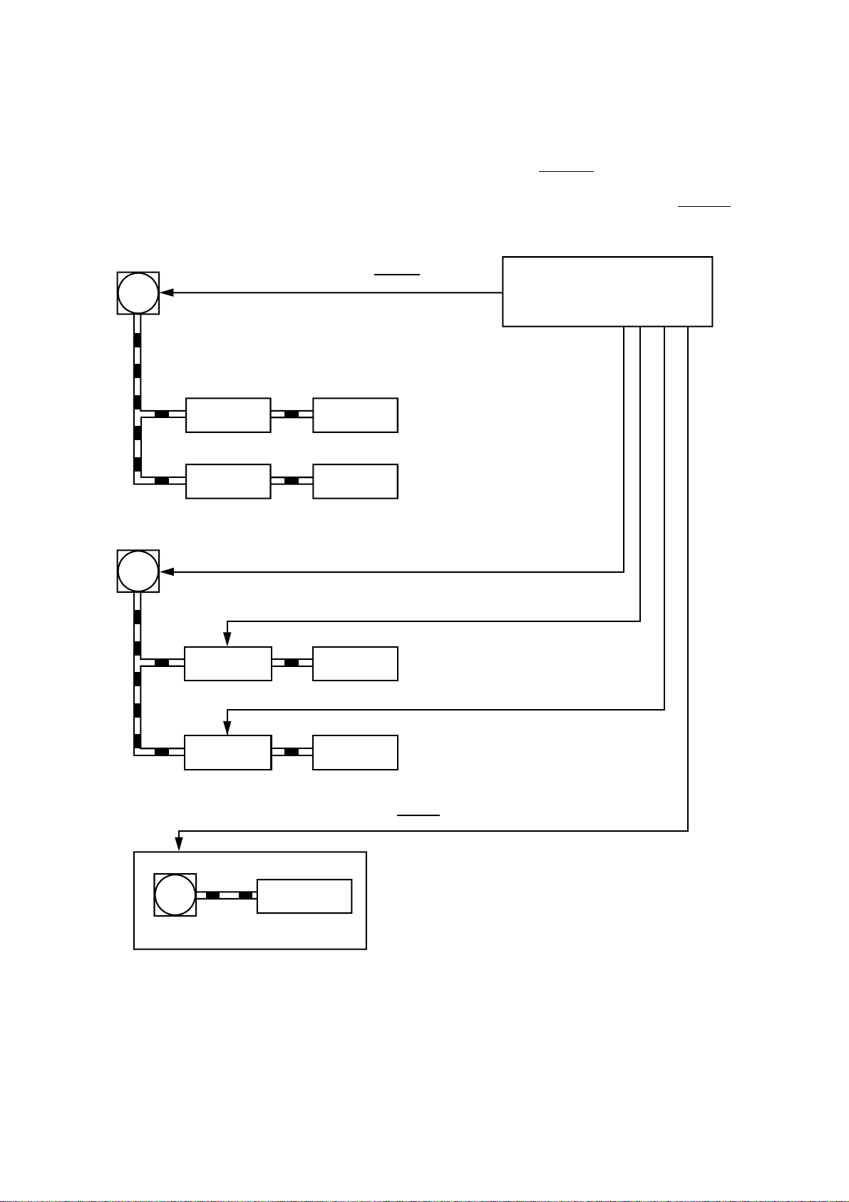
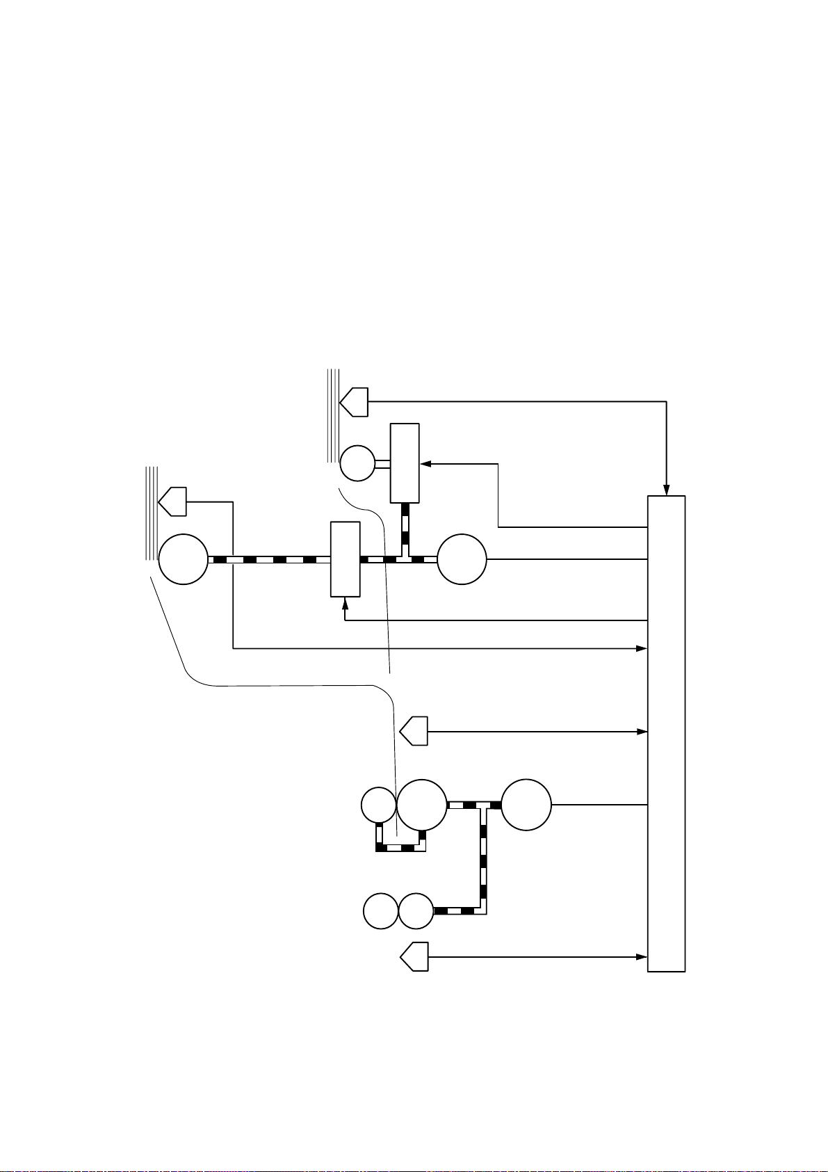
CHAPTER II THEORY OF OPERATION
This chapter describes the printer functions, the relationship between the electrical systems and
mechanical systems, and the timing of operations. Striped conduits ( ) indicate mechanical
linkages; solid thin arrows ( ) appearing with a signal name indicate the transmission of
single control signals and outlined thick arrows ( ) indicate the transmission of groups of
signals.
1. BASIC OPERATIONS
1.1 Mechanical Configuration
The printer functions can be divided into four blocks: the laser/scanner system, the image
formation system, the paper pick-up/feed system and the control system.
Expansion memory
(SIMM)
Control panel
Font cartridge/card
Main PCB
IMAGE FORMATION SYSTEM
Photosensitive drum
Cleaning unit
Optional I/O
(MIO)
External Device
CONTROL SYSTEM
Laser/scanner
unit
Developing
unit
Delivery rollers
PAPER PICK-UP/FEED SYSTEM
Fixing unit
Feeder
LASER/SCANNER
SYSTEM
Transfer
separation
unit
MP tray
Tray 1
Tray 2
(Option)
Figure 2.1
II - 1
Page 18
1.2 Main Drive
The power necessary for driving the printer is supplied by the main motor, the paper feed motor
and the scanner motor.
The main motor is controlled by the main motor drive signal (MDRIVE) output from the main
PCB, and the paper feed motor is controlled by the paper feed motor drive signal output from
the main PCB, and the scanner motor is controlled by the scanner motor drive signal (SDRIVE)
output from the main PCB.
Main motor
Main motor drive signal (MDRIVE)
Main PCB
Paper feed motor
Drum gear
Fixing unit
Paper feed motor drive signal
MP tray pick-up roller solenoid drive signal (MPSOL)
MP tray pick-up
roller solenoid
Tray1 pick-up roller solenoid drive signal (PUCL1)
Tray1 pick-up
roller solenoid
Photosensitive
drum
Paper delivery
rollers
MP tray
pick-up roller
Tray1
pick-up roller
Scanner motor
Scanner unit
Scanner motor drive signal (SDRIVE)
Note: There are cases, in the following pages, that
Scanning mirror
Figure 2.2
II - 2
a main motor is referred to as a DC motor, but
they are identical.
Page 19
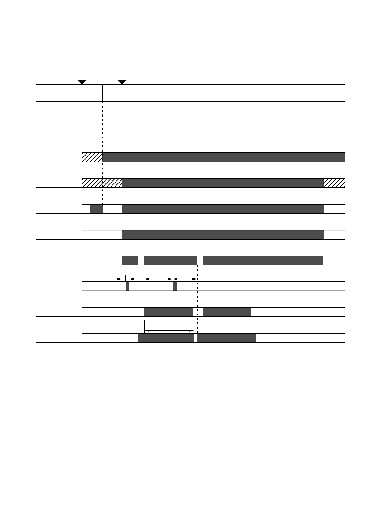
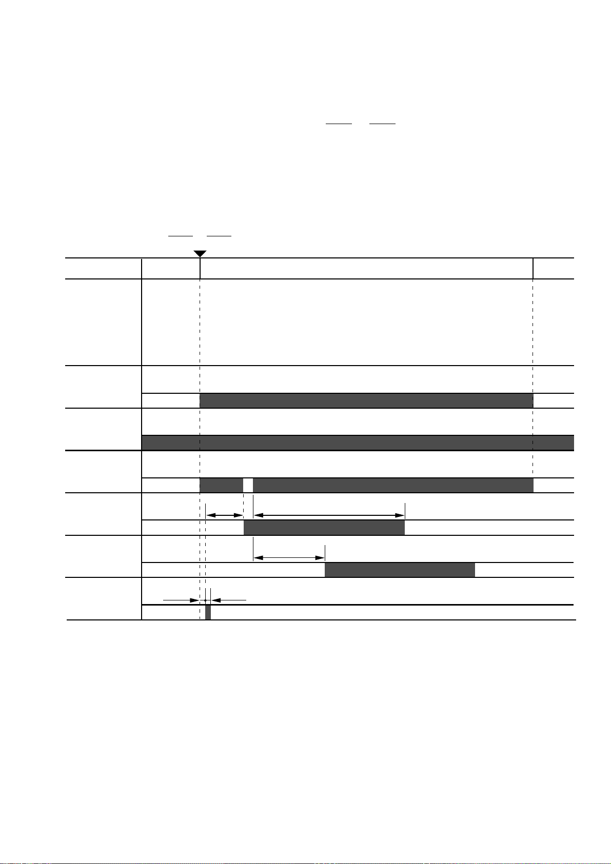
1.3 Basic Sequence of Operations
Power on Print
WAIT STBY PRINT
Ready lamp
Fixing heater
Main motor
170°C control 190°C
STBY
control
170°C
control
Scanner motor
Paper feed
motor
Pick-up roller
solenoid
Laser diode
Registration
sensor
0.2 sec
0.2 sec
2.5 sec
2.3 sec
4.24 sec
Timing for two consecutive prints on A4 paper.
Figure 2.3
II - 3
Page 20

2. LASER/SCANNER SYSTEM
To external device
SBD DATA VOFF
Collimator lens
Main PCB
Scanner driver
Cylindrical lens
Scanning mirror
Optical sensor
Figure 2.4
In response to the print signal transmitted from the external device, the main PCB generates the
drive signals (DATA,VOFF) for the laser diode and sends the signals to the scanner unit.
The laser diode in the scanner unit generates a laser beam modulated by DATA.
The modulated laser beam is aligned into a parallel beam by a collimator lens and a cylindrical
lens and then brought to the scanning mirror which is rotating at a constant speed.
The laser beam reflected by the scanning mirror focuses on the photosensitive drum via the
focusing lenses arranged in front of the scanning mirror.
The path of the beam coming through the focusing lenses is reflected by the reflective mirror.
Scanner motor
Focusing lenses
Beam detect mirror
As the scanning mirror rotates at a constant speed, the laser beam scans the photosensitive
drum at a constant speed.
As the photosensitive drum rotates at a constant speed and the laser beam scans the drum, an
images is formed on the drum.
II - 4
Page 21
3. IMAGE FORMATION SYSTEM
3.1 Outline
The image formation system is the main part of the printer. The print information, after input from
the video controller circuit into the engine controller circuit as a TVDO signal, forms a toner image
on the photosensitive drum.
Then the toner image is transferred onto the paper by the transfer charging roller. The image
formation system is composed of the photosensitive drum the charging unit, the developing unit
and the cleaning unit.
3.2 Printing Process
The major part of the image formation system is contained in the cartridge, as shown in Figure
2.5.
Laser beam
Cartridge
Primary charging roller
Cleaning blade
Photosensitive drum
Static charge eliminator
Blade
Developing cylinder
Paper
Transfer charging roller
Figure 2.5
The cartridge used by the printer has a seamless photosensitive drum with the structure shown
in Figure 2.6. The outer layer of the drum consists of an organic photoconductor (OPC); the base
is aluminum.
The printing process can be divided into five major stages:
Photoconductive layer
Figure 2.6
1. Electrostatic latent image formation stage
Step 1 Primary charge (-)
Step 2 Scanning exposure
2. Developing stage
Step 3 Development
II - 5
Base
Page 22
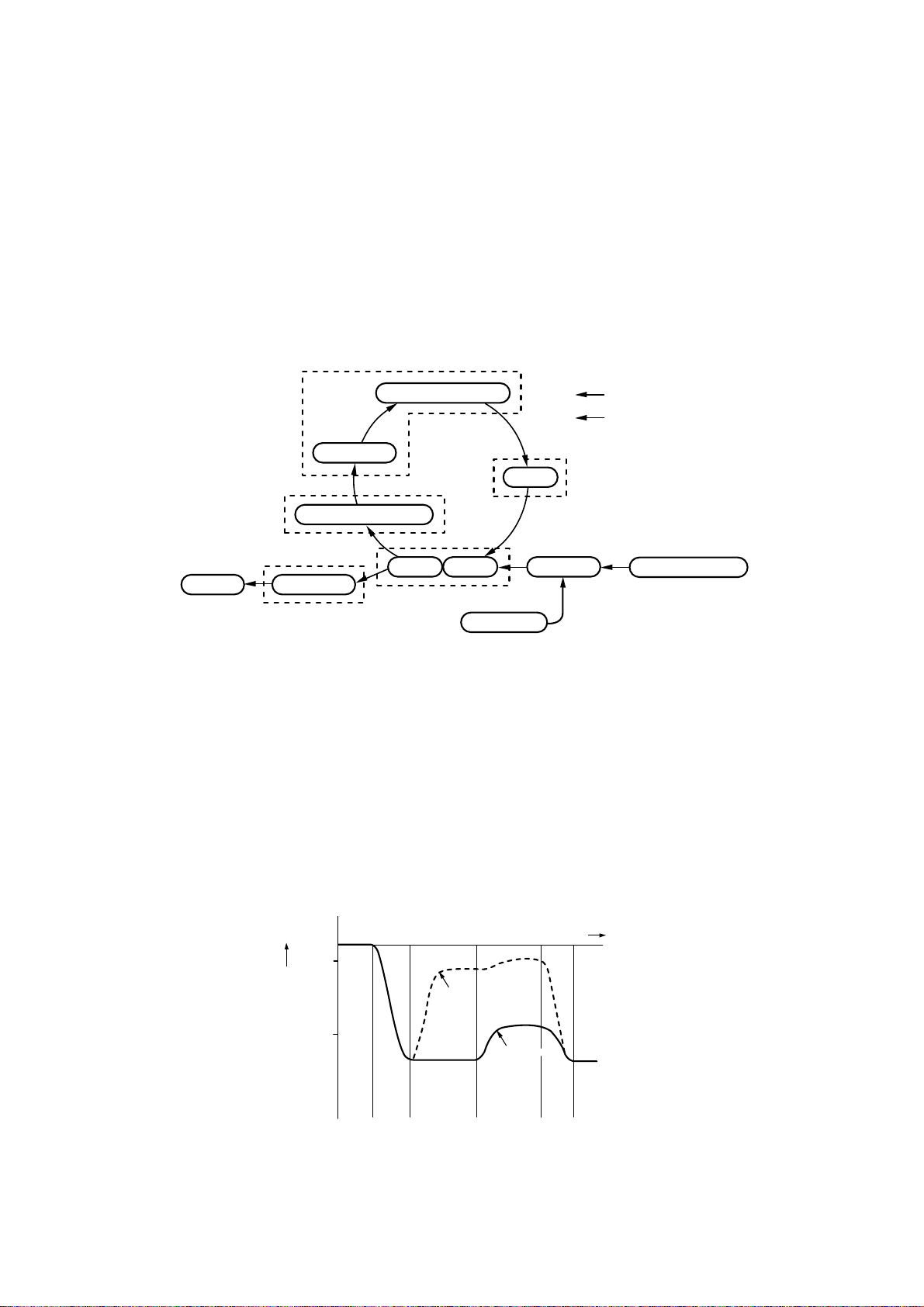
3. Transfer stage
Step 4 Transfer (+)
Step 5 Separation
4. Fixing stage
Step 6 Fixing
5. Drum cleaning stage
Step 7 Drum cleaning
Electrostatic latent image
formation stage
2. Scanning exposure
1. Primary charge
6. Fixing
7. Drum cleaning
5. Separa tion
4. Transfer
Drum cleaning stage
Fixing stage
Print delivery
Transfer stage
Figure 2.7
3.2.1 Electrostatic latent image formation stage
This stage has two steps, which together produce a pattern of electrical charges on the
photosensitive drum.
At the end of the stage, negative charges remain in the unexposed ”dark” area. Charges are
absent from the ”light” areas, where the laser beam struck (exposed) the drum surface.
Since this image of negative charges on the drum is invisible to the eye, it is called an
”electrostatic latent image”.
3. Develop
ment
Cassette feed
Developing stage
Registration
Paper path
Direction of drum rotation
Multi-purpose tray feed
0
-100
-500
Primary
Surface potential (V)
charge
(step 1)
Exposed
area
Scanning
exposure
(step 2)
Figure 2.8
II - 6
Time (t)
Unexposed
area
Transfer
(step 4)
Primary
charge
(step 1)
Page 23
Step 1 Primary charge
,,
,
,
,,
,,
,
,
,
,,
,,
,,
,
,
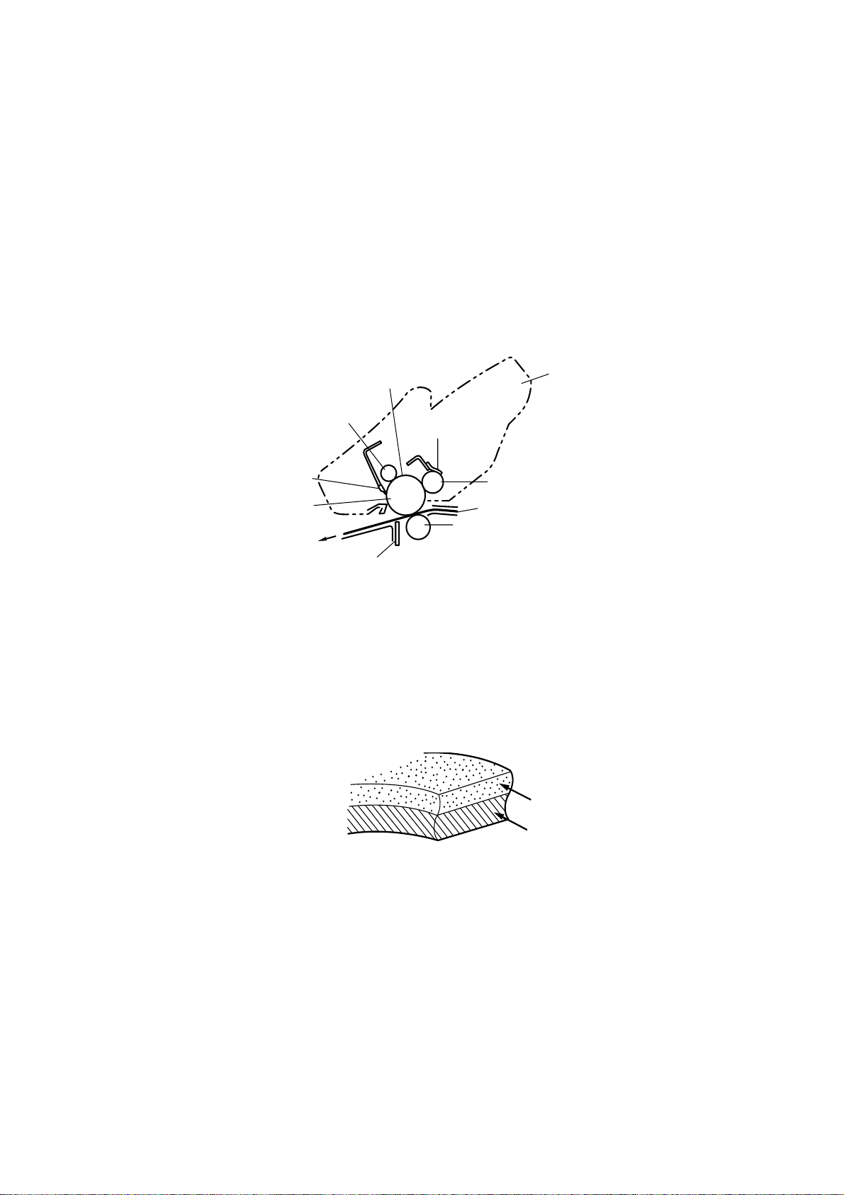
,,
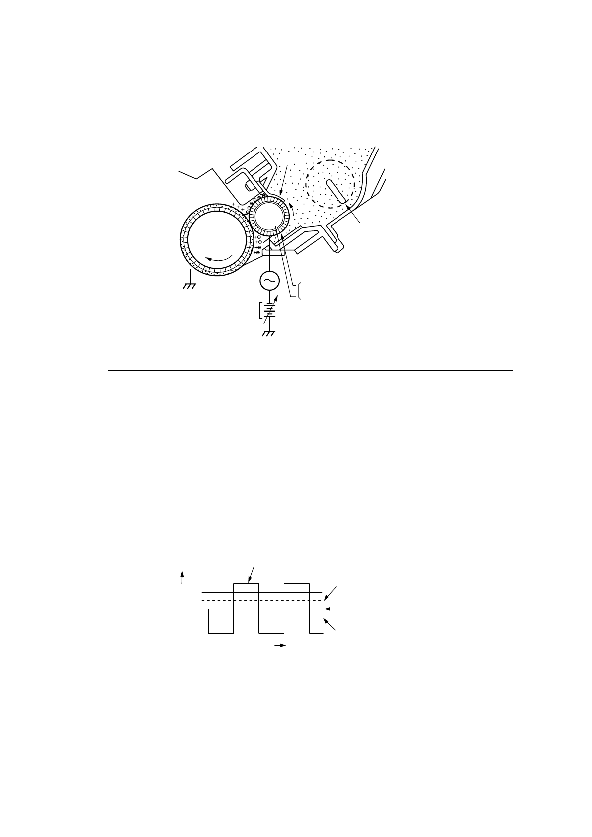
As preparation for latent image formation, a uniform negative potential is applied to the
photosensitive drum surface. The printer uses the charging method that directly charges the
drum for the primary charge.
The primary charging roller consists of conductive rubber. In addition to DC bias, AC bias is
applied to the primary charging roller to keep the potential on the drum surface uniform. This DC
bias is changed with the developing DC bias.
This charging method has advantages such as lower applied voltage, less ozone generation,
etc., compared with the corona charge system.
Primary charging roller
AC bias
Photosensitive drum
DC bias
Figure 2.9
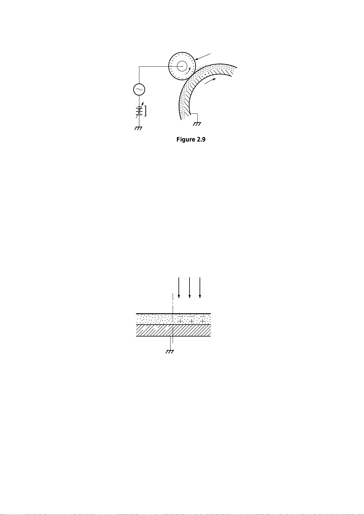
Step 2 Scanning exposure
Unexposed area
When the laser beam scans the drum surface, it causes the charge to be neutralized in the areas
struck by the beam. Areas on the drum with no charge form the electrostatic latent image.
Laser beam
___
+++
Exposed area
Figure 2.10
II - 7
Page 24
3.2.2 Developing stage
Development places particles of toner onto the areas of the drum that have been cleared of
charge by the laser beam. This makes a visible image. This printer uses the toner projection
development method with a single-component toner.
Step 3 Development
Blade
Photo-
sensitive
drum
AC bias
DC bias
Developing cylinder
Cylinder
Magnet
Stirrer
Figure 2.11
Note: The charges on the light areas on the photosensitive drum are shown as positive in this
figure. Actually they are negative, but they are more positive than the developing
cylinder and explanation is simplified by regarding them as positive.
As shown in Figure 2.11, the developing unit consists of a developing cylinder and rubber blade.
The developing cylinder rotates around a fixed internal magnet. The single-component toner
consists of magnetite and a resin binder, and is held to the cylinder by magnetic attraction. The
toner is an insulator, and acquires a negative charge by friction due to the rotation of the cylinder.
The areas on the drum that were exposed to the laser beam have a higher potential (are less
negative) than the negatively charged toner particles on the developing cylinder. When these
areas approach the cylinder, the potential difference projects the toner particles onto them. This
is called toner projection, and the latent image on the drum becomes visible.
Developing cylinder
surface potential
+V
0
-V
Voltage (V)
Time t
Drum surface
potential
(exposed area)
DC bias
Drum surface
potential
(unexposed area)
Figure 2.12
An AC bias is applied to the developing cylinder to help project the toner particles to the drum
surface and improve the contrast of the printed image. The center voltage of the AC bias (1600
Vp-p) varies with the DC bias voltage.
The IMAGE DENSITY ADJUSTMENT signal (sent from the Engine CPU to the high-voltage
power supply) changes the DC bias, and thus the potential difference between the cylinder and
drum. This changes the density of the print.
This printer has a stirring mechanism to supply toner in the cartridge smoothly to the cylinder.
II - 8
Page 25
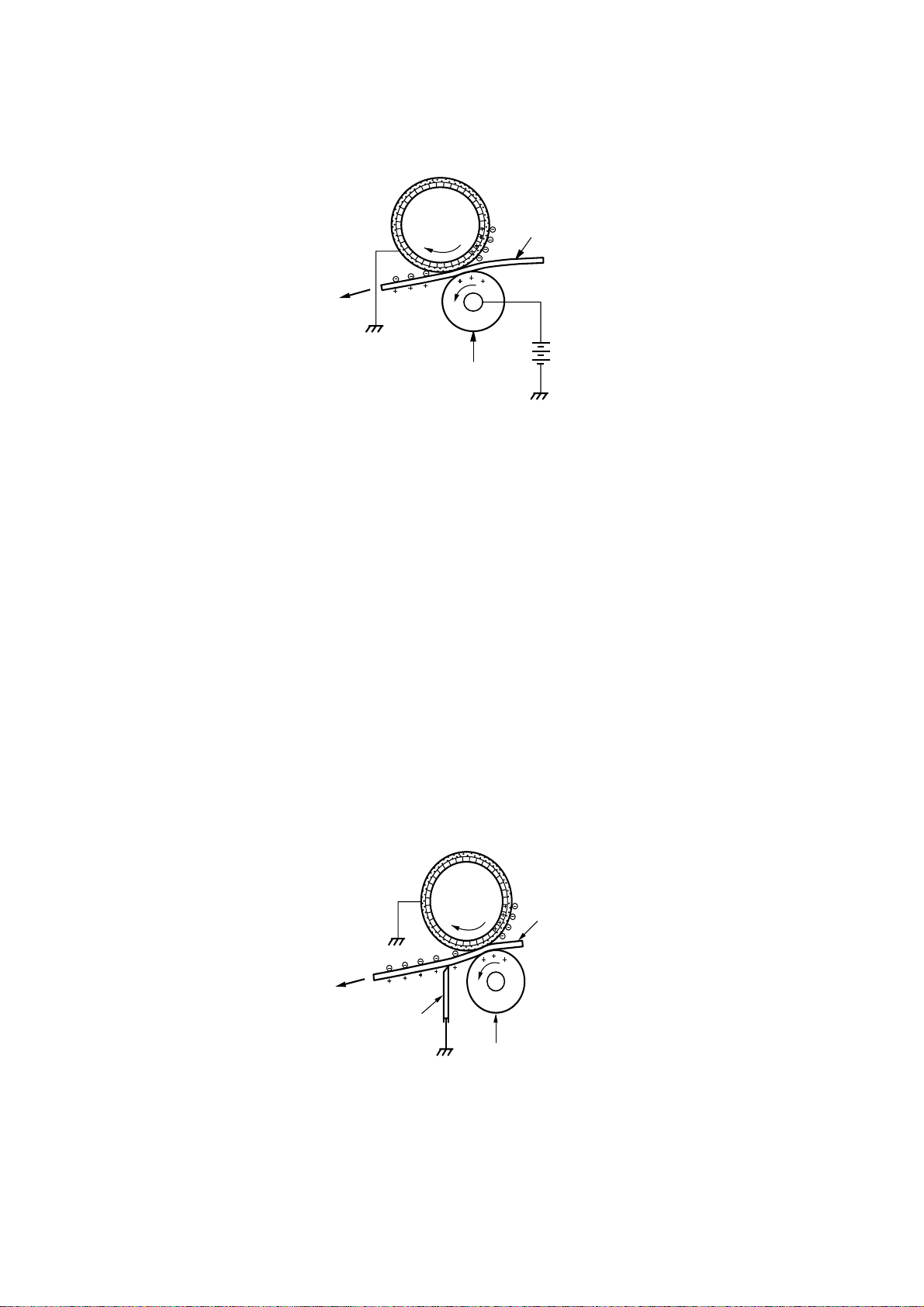
3.2.3 Transfer stage
In the transfer stage, the toner image is transferred from the drum surface to the paper.
Step 4 Transfer
A positive charge applied to the back of the paper attracts the negatively charged toner particles
to the paper. The printer accomplishes transfer by using the charging roller method. Advantages
compared with the corona transfer method are as follows:
Photo-
sensitive
drum
Transfer charging roller
Figure 2.13
Paper
• Low transfer voltage that is less than half that for corona transfer.
• Less ozone generation.
• The paper is supported by the transfer charging roller and photosensitive drum, so feed is
more stable.
Reference:
If the image on the photosensitive drum is not completely transferred to the paper due to
jamming, etc., the toner may adhere to the transfer charging roller. The printer removes the toner
from the transfer charging roller by switching the transfer voltage between positive and negative
in sequence. During wait, initial rotation, and last rotation, the printer sets the primary DC voltage
to zero, and sets the charge on the drum to zero. In this case, the transfer voltage is made
negative to remove the negatively-charged toner on the transfer charging roller to the drum. The
transfer charging roller is thus cleaned.
Step 5 Separation
Photo-
sensitive
drum
Paper
Static charge
eliminator
Transfer char
ging roller
Figure 2.14
The stiffness of the paper causes it to separate from the drum. (Curvature separation)
To stabilize the paper feed and prevent small white circles from appearing in the printed image
at low temperature and humidity, the charge on the back of the paper is reduced by the static
charge eliminator after transfer.
II - 9
Page 26
3.2.4 Fixing stage
The toner image transferred to the paper in the transfer stage is held only by electrostatic
attraction and slight physical adhesion, so even a light touch will smear the image.
In the fixing stage, the toner image is fixed by heating the paper and applying pressure. This
fuses the toner particles to the paper to make a permanent image.
Step 6 Fixing
The upper roller surface is PFA-coated. The upper and lower roller surfaces are grounded via
a diode to prevent the negative potential of the upper roller becoming higher than that of the
lower roller, resulting in the toner being drawn to the lower roller, and adhering to the lower roller
surface.
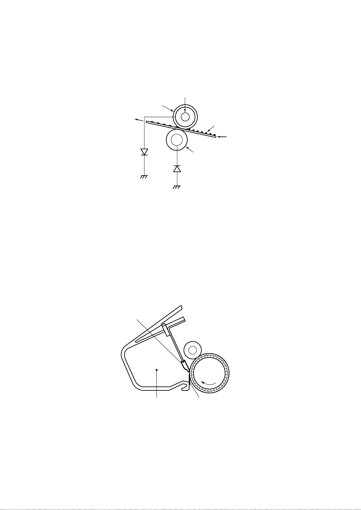
3.2.5 Drum cleaning stage
Halogen heater
Upper fixing roller
Toner
Paper
Lower fixing roller
Figure 2.15
In the transfer stage, not all the toner is transferred to the paper. Some remains on the
photosensitive drum. This residual toner is cleaned off in the drum cleaning stage so that the
next print image will be clear.
Step 7 Drum cleaning
Prior to the next printing, the residual toner on the drum surface is scraped away by the cleaning
blade to clean the drum surface. The removed toner is collected in the cleaner container.
Cleaning blade
Cleaner container
Photo-
sensitive
drum
Sweeper strip
Figure 2.16
II - 10
Page 27
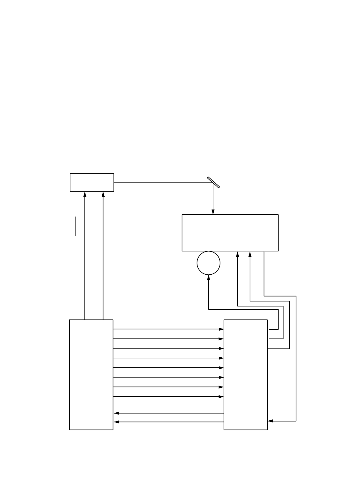
3.3 Operation
When the engine controller circuit receives a print signal (PRINT) or a pre-feed signal (PRFD)
from the video controller circuit, the engine controller circuit drives the main motor to rotate the
photosensitive drum.
After the drum surface is charged negatively by the primary charge roller, the laser beam
modulated by a DATA signal scans the drum surface to from a latent image on the drum.
The latent image formed on the drum surface is converted into a visible image by the toner on
the developing cylinder and then image is transferred onto the paper by the transfer roller unit.
Then the residual toner is removed from the drum surface with the cleaner blade.
The cartridge also has a toner sensor. When the output from this sensor falls below a certain
level, it warns that the EP-ED cartridge will be out of toner with an alarm.
Scanner unit
Reflection mirror
Laser beam
Laser diode drive signal (DATA)
Scanner motor drive signal (SDRIVE)
Primary charge (AC) drive (HV1AC)
Main
PCB
Primary charge (DC) drive (HV1DC)
Developing bias (AC) drive (DBAC)
Developing bias (DC) drive (DBDC)
Transfer charger 1 drive (HVT1)
Transfer charger 2 drive (HVT2)
Transfer charger 3 drive (HVT3)
Transfer charger 4 drive (HVT4)
EP-ED cartridge
Transfer
roller
High-voltage
power supply
PCB
Toner sensor signal 1 (TONER 1)
Toner sensor signal 2 (TONER 2)
Figure 2.17
II - 11
Page 28
4. PAPER PICK-UP/FEED SYSTEM
4.1 Outline
If a tray1 paper pick-up roller solenoid drive signal (PUCL1) is input to the circuit while the paper
feed motor is rotating, the paper pick-up solenoid comes on and the paper pick-up roller solenoid
is engaged. As a result, the paper pick-up roller rotates to feed paper down to the photosensitive
drum.
The paper position is controlled by the registration sensor so that the leading edge of the paper
is aligned with the leading edge of the image on the photosensitive drum. After this operation,
the paper is deliveried to the face down tray via the fixing unit. Paper ejection is detected by the
paper ejection sensor; if printed paper has not reached or not cleared the paper ejection sensor
in a specified time, the printer judges that a paper jam has occurred. In this case a paper jam
is noticed to the external devise by a status signal.
MP tray
paper empty sensor
MP tray paper empty sensor signal (PEMP)
Tray paper
empty sensor
Tray1 Pick-up
roller solenoid
Transfer roller
MP tray Pick-up
roller solenoid
Tray1 pick-up roller solenoid drive signal (PUCL1)
Tray1 paper empty sensor signal (PETRAY1)
Registration
Photosensitive
MP tray pick-up roller
solenoid drive signal (MPSOL)
Paper feed motor drive signal
Paper-
feed
motor
Registration sensor signal (REGIST)
sensor
drum
Main motor drive
signal (MDRIVE)
Main motor
Main PCB
Fixing rollers
Paper ejection sensor
Figure 2.18
II - 12
Paper ejection sensor signal (EJECT)
Page 29
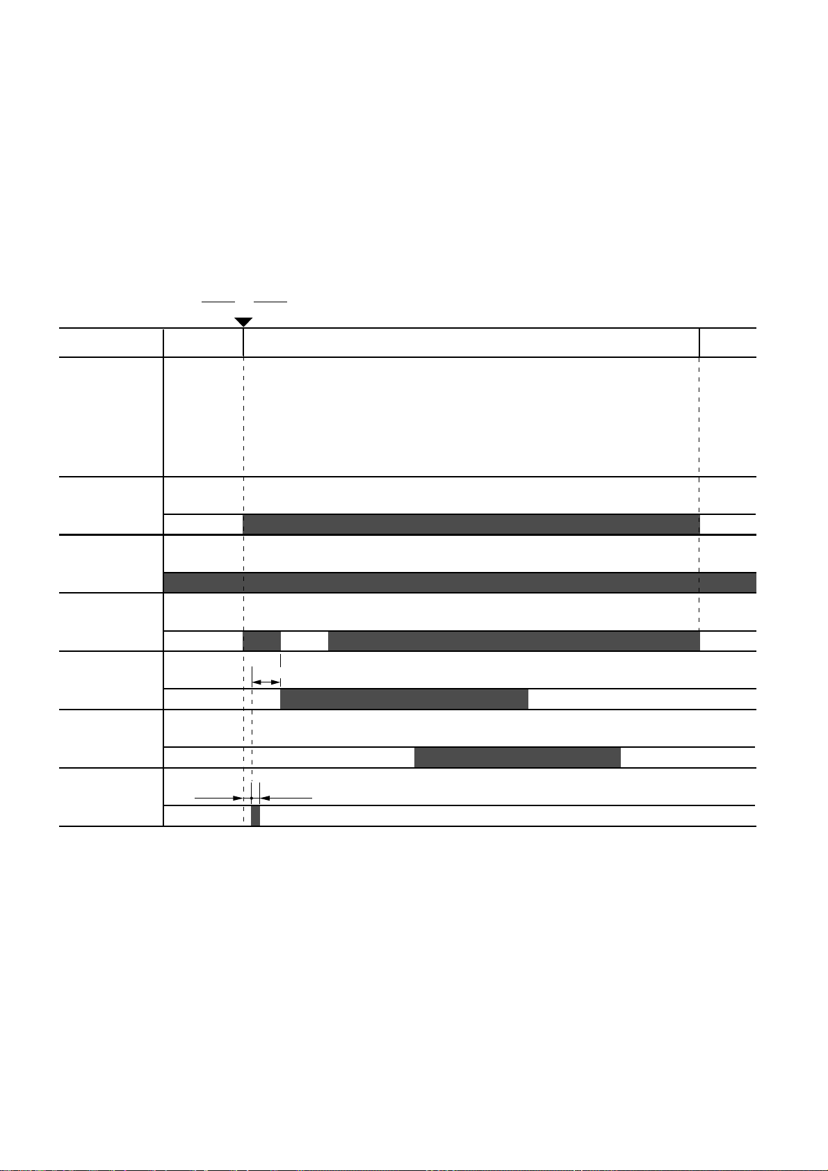
4.2 Cassette Feed
When the fixing rollers reach the specified temperature while a cassette with paper is in the
printer, the READY lamp changes from flashing to lighting.
When the engine controller circuit receives PRNT or PRFD signal from the video controller
circuit, the paper feed motor starts rotation. About 0.2 seconds later, the printer actuates the
tray1 pick-up roller solenoid and the pick-up roller makes one rotation. This feeds paper to the
photosensitive drum.
Timing chart for the pick-up one sheet
PRNT or PRFD
STBY PRINT STBY
Main motor
Paper empty
sensor
Paper feed
motor
Registration
sensor
Paper ejection
sensor
Pick-up roller
solenoid
0.2 sec
2.3 sec 4.24 sec
2.90 sec
0.2 sec
Figure 2.19
II - 13
Page 30
4.3 MP Tray Feed
The timing of the MP tray feed is identical to the timing of the cassette paper feed except for
the following points:
(1) The paper empty sensors are different.
Cassette feed : Tray1 paper empty sensor
MP tray feed
(2) The pick-up roller solenoids are different.
Cassette feed : Tray1 pick-up roller solenoid
MP tray feed
PRNT or PRFD
STBY PRINT STBY
: MP tray paper empty sensor
: MP tray pick-up roller solenoid
Main motor
Paper empty
sensor
Paper feed
motor
Registration
sensor
Paper ejection
sensor
Pick-up roller
solenoid
1.12 sec
0.2 sec 0.2 sec
Figure 2.20
II - 14
Page 31

4.4 Paper Jam Detection
The printer has a registration sensor and a paper eject sensor at the paper outlet to detect
whether the printed paper has been fed correctly. A paper jam is detected by whether the paper
is present at the sensor at the check periods programmed in the engine CPU memory. If the
engine CPU detects a paper jam, the main motor, paper feed motor and scanner motor is turned
off immediately and the jam status is transmitted to the video controller circuit.
A paper jam is detected in any of following conditions:
1) Paper exists at the paper ejection sensor or the registration sensor when power is
switched on. (JAM REAR or JAM INSIDE)
2) Paper has not reached the registration sensor within a specified time (JAM TRAYS).
3) Printed paper has not passed through the registration sensor within a specified time (JAM
INSIDE (1) ).
4) Printed paper has not reached the paper ejection sensor within a specified time (JAM
INSIDE (2) ).
5) Printed paper has not passed through the paper ejection sensor within a specified time
(JAM REAR).
Jam tray
STBY PRINT
Main motor
Pick-up
solenoid
Registration
sensor
Jam check
Main motor
Paper feed
motor
Jam inside (1)
STBY PRINT
5 sec5 sec
Figure 2.21
JamNormal
Registration
sensor
Jam check
Figure 2.22
II - 15
Normal
4.9 sec4.9 sec
Jam
Page 32

Jam inside (2)
Main motor
Paper feed
motor
Paper ejection
sensor
STBY PRINT
Jam check
Jam rear
Main motor
Paper feed
motor
Paper ejection
sensor
Figure 2.23
STBY PRINT
2.5 sec2.5 sec
JamNormal
9.56 sec
Jam check
9.56 sec
Figure 2.24
II - 16
JamNormal
Page 33

CHAPTER III ELECTRICAL SYSTEM
Electric signal levels are expressed by ”High” (approximate the supply voltage) or ”Low”
(approximate 0V). Signals with hyphen or slash, such as -FSRD or FSRD/, are low-active and
signals without hyphen or slash, such as FSRD, are high-active signals.
1. MAIN PCB
1.1 Outline
The Main PCB consists of the Video Controller Circuit and the Engine Controller Circuit.
The Video Controller Circuit performs the following functions.
(1) Converts data received from an external device, such as a personal computer, through
Centronics parallel interface or RS-232C serial interface into video data and transfers it
to the Engine controller circuit.
(2) Displays the current printer status in LED and LCD, and enables settings from the control
panel.
The operation sequence of the printer controlled by a microprocessor in the Engine Controller
Circuit. The Engine Controller Circuit outputs signals to drive the various loads on the laser
diode, scanner motor, main motor, etc. according to the print commands and image data from
the external device.
PC
PC
CDCC (bolse) IF
RS-232C IF
FONT
CARTRIDGE
IC CARD
(PCMCIA)
Video controller
ASIC
M65243FP
+24V
MIO BOARD
Engine controller
Regurator
MIO RELAY
(CONNECTOR)
PCB
Main PCB
Main CPU
79R3041
MASK ROM
16M mask 2 4MB
8M mask 2 2MB
DRAM
4M 4 2MB
DRAM (SIMM 3 slots)
24MBmax.
EEPROM
24CO4 4Kbit
ASIC
M65340FP (HRC/GSC)
Gate Array
µPD65626GF-176-3BA
(IO PORT. ENGINE)
Engine CPU
M38063
+24V
+5V
GND
CONTROL PANEL
Low-voltage
Power Supply
Figure 3.1 Main PCB Block Diagram
III - 1
Page 34

1.2 Video Controller Circuit
(1) CPU block
CPU(#26) IDT79R3041-20J manufactured by Integrated Device Technology
RISC chip
Clock speed: 19.6608 MHz
Appearance: 84-pin PLCC
(2) ASIC/Gate Array Block
• #32 M65243FP(Mitsubishi) - 208-pin QFP
Controls the address decoder, timers and interfaces (Centronics and RS-232C).
• #6 M65340FP(Mitsubishi) 80-pin QFP
Controls HRC(High Resolution Control), GSC(Gray Scale Control) and economy mode.
• #3 µPD65626GF-176-3BA(NEC) - 100-pin QFP
Controls the I/O ports and others.
(3) Font Cartridge/Card Block
• Font cartridge (option)
The font cartridge has a 32MB memory area and is controlled by the 16-bit bus.
The address bus a buffer LS244 and the data bus, a buffer LS245.
• Font Card (option)
The font card has a 32MB memory area and is controlled by the 16-bit bus.
The card is supplied with 12V power because the flash card requires 12V power supply when
writing or erasing data.
The address bus is buffered by LS244 and the data bus, is buffered by LS245.
(4) Centronics/RS-232C interface block
• Centronics parallel interface
Data transmission and reception are controlled by the M65243FP (#32).
• RS-232C
Data transmission and reception are controlled by the M65243FP (#32).
The ADM202JRN (#38) serves as driver/receiver.
(5) SIMM block
• SIMM (Single-Inline-Memory-Module) allows memory extension up to 26MB
• 3 SIMM sockets are available.
• SIMM should be of 72-pin type and its access time should be less than 70 ns.
• 4 types of SIMM (1MB, 2MB, 4MB and 8MB) can be combined:
1MB MH25632BJ-7 (MITSUBISHI), HB56D25632B-7A (HITACHI)
2MB MH51232BJ-7 (MITSUBISHI), HB56D51232B-7A (HITACHI)
4MB MH1M32EJ-7 (MITSUBISHI), HB56A132BT-7A (HITACHI)
8MB MH2M32EJ-7 (MITSUBISHI), HB56A232BT-7A (HITACHI)
1) The SIMMs have its printed marking on the PCB by silk screen: SLOT1, SLOT2 and
SLOT3, respectively. The SIMMs should be set in the order of SLOT1 - SLOT3.
2) SIMMs should be set in the order of its memory size and in the order of SLOT No.
Example: 3 SIMMs: 1MB, 2MB and 4MB
SLOT1 - 4MB
SLOT2 - 2MB
SLOT3 - 1MB
III - 2
Page 35

3) The attached Printer SIMM map shows the memory map for 4 SIMMs combined.
(6) ROM block
ROMs store the CPU control program and font data. ROMs are two 16Mbit masked ROMs and
two 8Mbit masked ROMs.
Optional sockets are available for two 8Mbit EPROM (µPD27C8000DZ-120 - NEC or equivalent) for expansion.
ROM access time should be less than 120nsec.
8Mbit EPROMs can be used instead of a 16Mbit masked ROM. To allow this substitution, the
soldering points SP5, SP6 and SP7 should be soldered and the cutting points CP2, CP3 and
CP4 should be cut.
(7) DRAM block
DRAMs are used for receiving buffer or working area of the CPU. The DRAM block contains
four 4Mbit DRAMs, thus having 2MB memory capacity in total.
The refreshing method is CBR (Cas Before Ras).
DRAM access time should be less than 80nsec.
III - 3
Page 36

0000_0000
0040_0000
0080_0000
0100_0000
0200_0000
ROM
(8MB)
Not used
(8MB)
Not used
(16MB)
0000_0000
0020_0000
0040_0000
0060_0000
0080_0000
Program ROM
(4MB)
Font ROM
(2MB)
Optional ROM
(2MB)
0400_0000
0600_0000
0800_0000
0B00_0000
0C00_0000
0E00_0000
0FC0_0000
0FD0_0000
(256MB)
MIO
(32MB)
Font card
(32MB)
Font cartridge
(32MB)
RAM
(MAX 48MB)
Not used
(16MB)
Peripheral I/O and
internal register
(32MB)
Not used
(approx. 32MB)
Boot ROM
0800_0000
0820_0000
09A0_0000
0B00_0000
0C00_0000
0C10_0000
0C20_0000
0C30_0000
0C40_0000
0C50_0000
0C60_0000
0C70_0000
0C80_0000
0C90_0000
0CA0_0000
0CB0_0000
0CC0_0000
0CD0_0000
0CE0_0000
Internal RAM
(2MB)
Expansion RAM
SIMM
(24MB max)
Not used
(22MB)
Inside M65243
µPD65626-176
Inside M65243
Inside M65243
Inside M65243
Inside M65243
M65340-0001FP
Not used
Not used
Inside M65243
Inside M65243
Inside M65243
Inside M65243
Not used
Figure 3.2 Memory map
III - 4
Page 37

ADDRESS
0820 0000
0830 0000
0840 0000
0850 0000
0860 0000
0870 0000
0880 0000
0890 0000
08A0 0000
123456789101112131415161718192021
NONE
1MB
2MB 2MB 2MB
1MB
1MB
1MB
2MB 2MB
1MB
1MB 1MB
4MB 4MB 4MB 4MB 4MB 4MB
8MB 8MB 8MB 8MB 8MB 8MB 8MB 8MB 8MB
2MB 2MB 2MB
1MB
4MB 4MB 4MB
1MB
2MB
08B0 0000
08C0 0000
08D0 0000
08E0 0000
08F0 0000
0900 0000
0910 0000
0920 0000
0930 0000
0940 0000
0950 0000
1MB
2MB
4MB
1MB
2MB 2MB
1MB
4MB 4MB 4MB
1MB
2MB
8MB 8MB 8MB 8MB
1MB
2MB
4MB
1MB
2MB
4MB
0960 0000
0970 0000
0980 0000
0990 0000
09A0 0000
8MB
Figure 3.3 SIMM map
III - 5
Page 38

DRAM block
SIMM block
Option I/F connector
ROM block
RS-232C serial I/F connector
Centronics parallel I/F connector
ASIC M65243FP
CPU(VIDEO)
C153
1
71
REV
8
7
72
C152
2
#21
C49
SLOT1
18
2
1
0P
P15
71
72
71
72
C151
SLOT2
C63C64
C62
2
1
1
R52R51 RA25 RA24
74F04
74F04
#20
R38
B48K158-3
C27
RA13 RA12 RA11
R17
C24
(25)
A25
B25
(50)
C150
SLOT3
2
74F04
C46C47
C61
GND VCC
CN4
12
C154
72
71
#41 #39
RA52
R88
1034
1034
RA44
PST591DMT
C143
C126
74ALS
C122
C116
74ALS
R92
R90
#42
R110
SP11
CP6
C121
R98
C113
C110
R89
#32
HM514800
HM514800
#30
HM514800
#27
CN3
C141
C120
14
1
ROM2H ROM1H
R121
R114
R120
R115
C140
R112
C139
R113
SP12
C123
C125
C127
R111
C124
ADM202JRN ADM202JRN
#36#37
42
(EVEN) (EVEN)
1
1
#35
42
1
#40
C112
C114
C109
#38
C98 C82
22
21
C91
42
1
C73
22
21 1
21 1
C90
42
SLOT4
R44
74LS244
RA15
CARTRIDGE
R29
C30
RA14
C65
R28
RA22
74LS244
R22
21
21
22
R50
C58
#26
#15
#16
R42
CP3
SP6
CP4
SP7
C32
C57
#25
R43
#14
SP5
CP2
21
22
#10
RA19
R123
74LS245 74LS245
C25
#6#7
ABCDEFGHJKL
0123456789
C13
94 96
M
R21
RA9
8MX6
SOLDER OUT
SP5
SP6
SP7
CP2
CP3
CP4
(1)
P5
A1
B1
(26)
LS08
#2
1
2
35
C2
36
HM514800
#22
2
1
74F04
#19
#17
C44
#11
74LS244
#12
R23
C29
RA18
RA10
C28
RA16
RA17
ROM0H
(EVEN)
C92
ROM0LROM1LROM2L
(ODD)(ODD)(ODD)
X24C04F
R3
CP1
LS74
25
13
19
P14
RS232C
RA39
1
CDCC
P13
RA55 RA54
R103
74F245D
74F245D
RA51
R106
RA48
RA45
RA42
#31
C106
Y1
RA58
RA57
RA56
C103 C101
49.3576MHz
RA41
42
RA53
R109
R97
RA50
RA49
#34
RA47
RA46
RA43
22 42
RA40
RA38
#29
C85
74F245D 74F245D
RA35
RA36RA34
RA33
C76
RA30 RA28
RA31 RA27
#23
C66
C16
(48)
C59
B16
22
(32)
A16
(16)
RA64
RA60
C142
C137
C138
R108
R107
R104
R102
104
105
C115
#33
C108
C104
R87
R84
156
R83
C96
157
R78
C95
R76
R73
C84
R64
SP8
R63
53
54
RA37 RA32
C78
C74
RA29
RA26
C70
74
75
#28
#24
R37
C42
R35
C43
C39
C38
C36
R34
1
80 65
64
C18
µPD65626
C6
R2
IC CARD
XT1
5.0MHZ
81
50
RA23
25
R24
40
C26
R20
R124
80
C12
R11
C9
51
RA21
RA20
SP4
C33
24
25
M65340FP
40
41
#8
R14
100
1
#4
C11
R10
#5
Q3
Q2
R4
R8
30
31
R7
R6 Q1
SP2
AN78N12
#3
13
C5
D1
C4
#1
C3
RA1
R1
SP1
P2
RA63
RA59
C134
C135
C136
C119
R69
R65
C68
#13
LS07
24
M38063E6FP
41
C23
C22
C21
C20
C19
C16
C15
C14
C10
R9
RA3
RA2
R119
C131
C132
C133
R105
C86
P8
C37
R19
R16
C17
RA4
P.FEED
P3
33
34
67
68
RA62
C130
R68
R3041
OPT IO
C45
C50
R30
R15
1
19
C1
RA61
C147
C148
C149
R118
C146
SP10
C118
M65243FP
C93C94
R67
R72
R62
C67
C41
R36
R33
R18
2
R13
2
1
C129
R75
D3
R32
L1
C7
+24B
+5B
20
+5V
+24V
C144
C145
/RESET
53
208
C89
R70
R71
33
R46
R41
R26
1
64
R79
D2
Q5R12
R100
C117
C87
R66
11
R45
R40
Q6
C128
1
R122
R116
R117
R99
52
R94
R86
R85
C97
R77
R74
32
C79 R57
R53
C71
12
#18
UPC
358
R39
Q14
80
#9
65
8
SP3
+24VRET
1
P1
SP9
C107
C88
R31
R27
C34
FLOCK
GND
GND
+24V
HEAT
Q4
R125
R59
R56
C75
C48
+5V
+5V
7
C105
C102
C99
C53
R25
C31
PANEL
C100
R55
36
18
CN2
1
R101
D7
CP5
R58
R48
C56
1
D8
R95
R93
R96
R91
C111
R81
Q18
Q19 Q17
3
D6
1
D4
4
C81
C83
R61
C80
R60
1
C77
4
C72
R54
C69
Q15
1
6
P9
(33)
C1
C60
(17)
2
B1
A1
(1)
4
R49
C55
R47
C54
C52
1
C51
15
C40
P6
H.VOL
C35
Q12
Q13 Q10
Q11 Q9
Q8 Q7
1
BZ1
3
CN1
RC
1
Y2
39.3216MHZ
R82
R80
Q16
FAN
P12(WHITE)
D5
(WHITE)
P11
FUSER
SCNMTR
P10
SCNLSR
1
(RED)
P7
MTR
16
2
CPU(ENGINE)
P4
POWER
C8
S1
20
21
Font cartridge connector
Control panel connector
Font card connector
ASIC µPD65626
ASIC M65340 FP
Figure 3.4 Main PCB
III - 6
Page 39

1.3 Engine Controller Circuit
Scanner Unit
Primary charging roller
Engine
Controller
Circuit
High-Voltage
Power Supply
Assy
Paper Feeder
PCB
Detectors
Main Motor
Low-Voltage
Power Supply
Assy
Transfer roller
Developing cylinder
Toner sensor
Pick-up Solenoid
MP Tray Pick-up Solenoid
Pick-up Motor
Fixing Unit
Figure 3.5 Engine Controller Block Diagram
Components in the Circuit (refer to the next page)
A. Engine Control CPU
B. Low-Voltage Power Supply Connector
C. Fuser Unit Control
C-1. Heater Drive Circuit
C-2. Heater Temperature Input Signal
C-3. Paper Eject Input Signal
D. Paper Feeder PCB Control Signals and Connector
E. Option Interface Circuit and Connector
F. High-Voltage Power Supply Control Circuit and Connector
G. Scanner Unit Control
G-1. Scanner Motor Control Circuit
G-2. Laser Diode Drive PCB Control Circuit
H. Fan Motor Drive Circuit
I. Main Motor Control Circuit
J. Cover Open Detect Circuit
K. Safety Door Switch Circuit
III - 7
Page 40

F
D
C-2
C-3
E
A
J
C
C-1
K
B
Figure 3.6 Main PCB Circuit
III - 8
I
H
G
G-1
G-2
Page 41

2. PAPER FEED DRIVE CIRCUIT
A. Connector to Main PCB
B. Pick-up Motor Drive Circuit and Connector
C. Pick-up Solenoid Drive Circuit and Connector
D. Multi Purpose Tray Pick-up Solenoid Drive Circuit and Connector
E. Sensors
E-1. Tray1 Paper Empty Sensor
E-2. Multi Purpose Tray Paper Empty Sensor
E-3. Regist Sensor
E-4. Pre-Regist Sensor
E-5. Paper Detect Sensor in Duplex Unit
F. Tray1 Paper Size Detect Switches
Refer to the next page.
III - 9
Page 42

F
B48K140-1
MT B
MT A
2
5
P1(FEED MOTOR)
#1
SW1
4
P1(SIZE)
MT D
MT C
6
1
8181117
OUTA
INA
SLA7027M
6175162
SW2
3
PSIZE1
+24VB
OUTB
OUTAN
INB
INAN
SW3
2
PSIZE2
+24VB
3
+24VB
VSSA
OUTBN
INBN
TDA
±0V
SW4
1
PSIZE3
PSIZE4
+24VB
4
C1
100µ-35V
+
C2
103
0V
12314415
VSSB
GNDA
GNDB
TDB
RSA
13910
5
0V
REFA
RSB
+5V
REFB
+24VRET
R10
MP-SOL
1
2
P4 (MP SOL)
R11
27
R12
82
±0V
1K
R6
1-1W
C5
222
R7
2.2K
R4
C4
222
2.2K
R5
1-1W
Q1
+24VRET+24VRET
DTC114ES
(* -02D) HLD
±0V
Q2
2SC5060
CA-SOL
1
2
P3 (CA SOL)
+24V +24V
+24V +24V
D
R15
4.7K
+24VRET
+24VRET
B
B48K139-1
P5(ENGINE)
796820
ABC
D
FE-MT
FE-MT
FE-MT
FE-MT
+5V
19
CA SOL
+5V
R2
3
PF-PE
MP SOL
470
PH2
R3
47K
R8
47K
E-1
±0V
±0V
R14
14
+5V
470
PH5
MP-PE
C3
C6
E-2
R1
±0V
±0V
471
471
+5V
5
REGIST
470
PH1
E-3
±0V
±0V
+5V
R13
470
13
PREREG
E-4
±0V
PH4
±0V
Q3
2SC5060
0V
C
R16
4.7K
PSIZE1
PSIZE2
PSIZE3
SIZE1
SIZE2
243
171516
SIZE3
PSIZE4
1
18
SIZE4
5
±0V 0V
F
HLD (* -05D)
+24VB
11410
HOLD
+24VB
+24VRET
+5V
12
+5V
+24VRET
±0V
1
0V
R9
2
+5V
DUPE
E-5
470
PH3
P2(SIZE)
±0V
±0V
Figure 3.7 Paper Feed/Size-SW PCB Circuit
A
III - 10
Page 43

3. DISPLAY CIRCUIT
3.1 Outline
The control panel of this printer has four LED lamps, one LCD display, and eight switches.
The control panel is connected to the Main PCB and its functions are as follows:
(1) The LCD shows the printer status and error message in alpha-numeric characters.
(2) The LED lamps indicate the operating conditions of the printer.
(3) The printing mode and LCD brightness can be changed by switches.
LCD
LED1
LED2
SW8 SW7 SW6 SW5 SW4 SW3 SW2 SW1
LED3
LED4
)
PAD4-PAD7
LED2 (READY)
3.2 Operation
Indicators on the control panel (LED lamps and LCD) are controlled by the video controller
circuit.
All the switch signals are input to the video controller circuit.
Signals Descriptions:
LED1 - LED4 On-off control for the respective LED lamps.
PAD4 - PAD7 LCD control signal.
LCDRS A signal to distinguish PAD4 - PAD7 into command and data.
LCDE A signal to start the operation.
SW1 - SW8 Input signals from the switches.
LED3 (DATA)
LED4 (ALARM)
FORM FEED
LCDE, LCDRS
LED1 (ONLINE)
SW8 (SEL)
Main PCB
SW7 (MODE)
SW6 (FONT)
SW5 (
Figure 3.8 Display Circuit
Illuminating when Low and extinguished when High.
Going Low when each switch is pressed.
SW4 (SET)
SW3 (CONTINUE)
SW2 (DOWN)
SW1 (UP)
III - 11
Page 44

4. LOW-VOLTAGE POWER SUPPLY ASSY
4.1 Outline
The low-voltage power supply assy consists of the low-voltage generating block (hereinafter the
DC block) and the heater drive circuit block to turn the heater on (hereinafter the AC block).
When the power switch (SW1) is turned on, AC power is supplied to the low-voltage power supply
assy.
The DC block generates +5 VDC, and +24 VDC.
When the heater is turned on, AC power is supplied to the AC block under control of the heater
on-off signal from the engine controller.
+24V output is reserved in the DC block, for the cooling fan for the low-voltage power supply
assy.
4.2 Protection Functions
Each of the power supply circuits, +5V, and +24V, has a protection function to prevent the circuit
from accident by automatically cutting off the power supply in the case of a over-voltage or overcurrent of the load.
When the cooling fan stops to rotating, an over-voltage protection or a short-circuit protection
function is activated, and all the DC power supplies are cutoff.
In this case check and clear the cause on the load after turning the power switch (SW1) off, and
then switch the power on again at least one minute after the power shut-down.
III - 12
Page 45

P3
HEAT/
1
+24V
4
Rectfier
Transformer
+5V
+5V
2
3
Chopper
±0V
+24VRET
6
5
±0V
7
Over
FANLOCK/
8
Voltage
Detector
Feedback Control
AC IN
H1TH1
Lamp
Thermal
Fuse
Heater
21
To Heater Circuit
P1
F101
L
Control
N
Inlet
F102
L
Rectfier
Noise
Filter
Power
Switch
N
(SW1)
Figure 3.9 Low-Voltage Power Supply PCB Block Diagram
III - 13
Page 46

5. HIGH-VOLTAGE POWER SUPPLY ASSY
5.1 Outline
The High-Voltage Power Supply Assy supplies the high-voltage for the charging roller, the
developer cylinder and the transfer roller according to the engine CPU’s control signals.
The block diagrams are shown Fig 3.10 and 3.11.
5.2 Operation of the Components of the High-Voltage Power Supply Assy
(1) Primary charging
When input signal/HV1AC gets the Low level, the primary high-voltage AC is applied to the
primary charging roller. And when input signal/HV1DC gets the Low level, the primary highvoltage DC is applied to the primary charging roller. The primary high-voltage DC changes with
developer bias DC according to values of the input signal DNSTY which is for print density
adjustment.
(2) Developer bias
When input signal/DBAC gets the Low level, the developer bias AC is applied to the developer
cylinder. And when input signal/DBDC gets the Low level, the developer bias DC is applied to
the developer cylinder. The developer bias DC changes according to values of the input signal
DNSTY which is for print density adjustment, like the primary high-voltage DC.
(3) Transfer charging
Transfer bias is controlled by the input signals HVT1 - 4 and HVTFB. When the input signal/
HVT1 gets the Low level, negative high-voltage is applied to the transfer roller. When the input
signal/HVT2 gets the Low level, positive high-voltage is applied to the transfer roller. When the
input signal/HVT3 gets the Low level, positive high-voltage about 1100 times that of the input
signal HVT4 is applied to the transfer roller. The input signal HVTFB has voltage about 1/1100
times the positive voltage generated on the transfer roller. Once the engine CPU is informed of
this voltage, the bias applied to the transfer roller can be known.
Note: The HVT2 signal generates high-voltage irrespective of the HVT4 signal.
(4) Toner sensing
Voltage levels of the input signals TONER1 and TONER2 allow the engine CPU to check if the
cartridge is set or not and if toner is empty. The TONER1 carries the voltage generated at the
toner sensor and the TONER2 carries the developing bias output value.
III - 14
Page 47

PRIMARY HIGH-VOLTAGE AC
High-Voltage
Electrode
/HV1AC
DNSTY
/HV1DC
/DBAC
/DBDC
P4
1
5
2
3
4
Sin Wave
Generator
PRIMARY HIGH-VOLTAGE DC
Pulse
Generator
PULSE
DEVELOPER BIAS AC
Current
Buffer
Control Unit
(Feedback Circuit)
(ON / OFF Circuit)
Current
Buffer
Current
Buffer
Control Unit
(Feedback Circuit)
(DNSTY Control Circuit)
(ON / OFF Circuit)
P1
DBOUT
High-Voltage
Electrode
Pulse
Generator
PULSE
Current
Buffer
Control Unit
(Feedback Circuit)
(ON / OFF Circuit)
DEVELOPER BIAS DC
Current
Buffer
Current
Buffer
Control Unit
(Feedback Circuit)
(DNSTY Control Circuit)
(ON / OFF Circuit)
P2
Figure 3.10 High-Voltage Power Supply Block Diagram 1
III - 15
Page 48

TRANSFER HIGH-VOLTAGE
Pulse
Generator
Current
Buffer
High-Voltage
Electrode
P5
/HVT3
/HVT2
HVTFB
HVT4
/HVT1
TONER1
TONER2
0V
24VRET
+5V
P4
10
11
13
12
14
15
Attenuator
Current
Buffer
Constant Current
Control Unit
(Feedback Circuit)
(ON / OFF Circuit)
8
7
9
Constant Voltage
Control Unit
(HVT4 Control Circuit)
6
Pulse
Generator
Current
Buffer
+24V
16
TONER SENSE
Toner Sense
Control Unit
(Toner 1 Circuit)
(Toner 2 Circuit)
Figure 3.11 High-Voltage Power Supply Block Diagram 2
Toner Sense
Electrode
P3
DBOUT
III - 16
Page 49

CHAPTER IV MECHANICAL SYSTEM
Safety Precautions
To prevent the creation of secondary problems by mishandling, observe the following precautions during maintenance work.
(1)
Always turn off the power before replacing parts or units. When having access to the power
supply, be sure to unplug the power cord form the power outlet.
(2) Be careful not to lose screws, washers, or other parts removed for parts replacement.
(3) Be sure to apply grease to the teeth of gears.
(4)
When using soldering irons and other heat-generating tools, take care not to damage
resin parts such as wires, PCBs, and covers.
Before handling the PCBs, touch a metal portion of the equipment to discharge static
(5)
electricity, or the electronic parts may be damaged due to the electricity charged in your
body.
(6) When transporting PCBs, be sure to wrap them in conductive sheets such as aluminum
foil.
(7) Be sure to reinsert self-tapping screws correctly, if removed.
(8) Unless otherwise specified, tighten screws to the torque values listed below.
Tapping screws
•
S tight M3 : 7kgf
B tight M3 x 6 : 5kgf
M3 x 8 : 7kgf
Stepped screws
•
M3 : 7kgf
M4 : 10kgf
(9) When connecting or disconnecting cable connectors, hold the connector bodies not the
cables. If the connector has a lock, always slide the connector lock to unlock it.
(10) After repairs, check not only the repaired portion but also that the connectors and other
related portions function properly before operation checks.
•
cm
•
cm
•
cm
•
cm
•
cm
the
Notes
On the next page is a disassembly order flow which helps you access the object
•
component.
Unless otherwise specified, the disassembled parts or components should be
•
reassembled in the reverse order of removal.
IV - 1
Page 50

PRINNTER DISASSEMBLING PROCEDURE
EP-ED CARTRIDGE
PRINTER BODY
1
TONER CARTRIDGE LID
PAPER TRAY
PAPER DELIVERY HOLDER SPRING
2
SIDE COVER L
3
FONT COVER ASSY
4
UPPER COVER ASSY
5
REAR COVER ASSY
6
SIDE COVER R
MIO LID
DC FAN MOTOR
7
HOLDER
SIMM REPLACE LID MIO BOX
PCB HOLDER
8
MAIN PCB
9
CONTROL PANEL UNIT
DC FAN MOTOR
13
FIXING UNIT
14
TRANSFER UNIT
CARTRIDGE GUIDE R
GROUND LEAF SPRING
PANEL ARM L,R
HEAT INSULATION COVER
LV HARNESS 8P
15
DC GEAR HOLDER ASSY
16
PS SWITCH WIRE
17
REMOTE SWITCH
18
HIGH-VOLTAGE POWER SUPPLY PCB ASSY
BEAM
10
SCANNER UNIT
DUCT, CARTRIDGE GUIDE L
CARTRIDGE LOCK SPRING L.R,
HOLD ROLLER
11
CARTRIDGE STOPPER ASSY
SCANNER HOLDER ASSY
FEED FLAT CABLE 20P
12
PAPER FEED CHASSIS UNIT
19
LOW-VOLTAGE POWER SUPPLY PCB ASSY
CHASSIS
IV - 2
Page 51

PRINTER BODY
1.1 Configuration
Upper cover assy
Side cover L
Control panel unit
Paper tray
Font cover assy
Figure 4.1
1.2 Toner Cartridge Lid
(1) Remove the supporter from the toner cartridge lid.
(2) Remove the toner cartridge lid from the upper cover.
Toner cartridge lid
Toner cartridge lid
Rear cover assy
Side cover R
Open the toner
cartridge lid
Upper cover assy
Supporter
Figure 4.2
1.3 Side Cover L
(1) Release the lock by pinching the lever on the left top surface ( A ) and remove the cover
by pulling it rearward ( B ).
Cleaner brush
A
B
Side cover L
Hook lever
Figure 4.3
IV - 3
Page 52

1.4 Font Cover Assy
(1) Remove the font cover assy by loosening the screw on the top and releasing the hooks
on the bottom and the side.
Hook
Figure 4.4
1.5 Upper Cover Assy, Rear Cover Assy
1.5.1 Upper cover assy, rear cover assy
(1) Loosen the 4 screws on the rear (the upper 2 screws secure also the upper cover ).
Screw
Hook
Font cover assy
A
Upper cover assy
Screws
B
Rear cover assy
Screws
Figure 4.5
(2) Loosen the top left screw.
(3) Remove the upper cover assy ( A ) (Refer to Figure 4.5).
(4) Remove the rear cover by pulling it rearward ( B ) (Refer to Figure 4.5).
Upper cover assy
Screw
hook
Figure 4.6
IV - 4
Note: The hook is released automatically
by removing the upper cover assy
in the direction of the arrow.
Page 53

1.5.2 Changeover guide, jam remove cover
(1) Open the jam remove cover by hooking your finger on 2 dents ( A ).
(2) Remove the jam remove cover with its center part opened by bending the arm of the
boss both on sides ( B ) toward the front ( C ).
(3) Remove the changeover guide from the boss by bending the right hook (viewed from the
rear) of the rear cover ( D ), then remove the changeover guide ( E ).
Rear cover assy
Changeover guide
Jam remove cover
1.6 Side Cover R
A
Dents
Figure 4.7
Hole
Boss
D
E
B
C
(1) Remove the side cover R by releasing the 4 hooks.
Front
Figure 4.8
Rear
Side cover R
Hook at 4 places
Note: Before releasing the 4 hooks, remove
the paper tray.
IV - 5
Page 54

1.7 DC Fan Motor
(1) Remove the DC fan motor from the DC fan motor holder by loosening the two screws.
(2) Loosen the screws securing the PCB holder and remove the entire DC fan motor holder.
(3) Remove the fan harness connector from the main PCB assy.
Screw
Fan connector
Figure 4.9
1.8 Main PCB
Note: If replacing the main PCB with a new one, follow the step in the attached insertion
sheet with the new main PCB to install it.
(1) Remove the SIMM replace lid.
DC fan holder
Screws (yellow)
SIMM replace lid
2 screws
DC fan motor
Figure 4.10
(2) Remove the MIO box.
MIO box
Screws
Figure 4.11
IV - 6
Page 55

(3) Remove the PCB holder by loosening PCB holder fixing screws, 2 centronics connector
screws and 2 RS-232C connector screws.
PCB holder
Screws
Figure 4.12
(4) Remove the switch flat cable 21P and the feed flat cable 20P.
(5) Remove the fan harness 3P, the fuser harness 4P, the SCN harness 4P, the SCN flat cable 6P,
the DC motor harness 4P, the HV harness 16P and the LV harness 8P.
SCN harness 4P
Fan harness 3P
Fuser harness 4P
SCN flat cable 6P
Feed flat cable 20P
(6) Remove the main PCB assy.
7 screws
DC motor harness 4P
HV harness 16P
LV harness 8P
Switch flat cable 21P
Figure 4.13
Main PCB assy
Figure 4.14
IV - 7
Page 56

1.9 Control Panel Unit
Switch flat cable 21P
Screws
Pin
Control panel unit
Panel arm L
Main PCB
Figure 4.15
(1) Remove the left side the control panel from the arm L by loosening the screws of the panel
arm L.
(2) Remove the switch flat cable 21P from the main PCB.
(3) Remove the control panel from the right panel arm R pin by sliding the control panel to the right.
C
D
A Tilt the control panel unit.
B Pinch the lever.
C While pinching the lever,
A
B
rotate, downward toward
you, the control panel unit on
the right pin taken as a fulcrum.
D Remove the control panel
unit.
Figure 4.16
(4) Release the panel sheet 8 hooks to remove the panel sheet from the control panel.
8 Hooks
Control panel unit
TEST
CONTINUE
SET
RESET
SHIFT
FORM FEED
COPY
FONT
MODE
FEEDER
ON LINE
SEL
ECONOMY
EMULATION
READY
DATA
DUPLEX
COPY PAGES
ORIENTATION
ALARM
FEEDER
Panel sheet
Figure 4.17
IV - 8
Page 57

1.10 Scanner Unit
(1)
Unplug the LD PCB harness (scanner flat cable) connector (6P), and SCN harness connector
(2) Remove the beam from the body by loosening the screws.
(3) Remove the scanner unit from the body by loosening the screws.
Caution: Do not disassemble the scanner unit, it can be only adjusted at the factory.
Scanner unit
Screws
SCN harness 4P
connector
Scanner flat cable 6P
connector
Figure 4.18
Screws
1.11 Cartridge Stopper Assy
(1)
Loosen 4 screws and remove the scanner mount plate in the direction of the arrow (the
leaf spring is also released at the same time.)
(4P).
Beam
ground
(2) Release the hook by bending the arm of the cartridge stopper assy ( A ), slide the cartridge
stopper assy to the left ( B ) and the remove the cartridge stopper assy ( C ).
Rear
Scanner mount plate
Left side
Scanner mount plate
Ground leaf spring
Cartridge stopper assy
Figure 4.19
Cartridge stopper assy
Screws
Right side
Front
B
C
A
Figure 4.20
IV - 9
Page 58

1.12 Paper Feed Chassis Unit
(1) Pull out the unit by loosening the 8 screws (4 screws for front and 4 screws for bottom).
Paper feed chassis unit
Screws
Screws
Note: When installing the paper feed chassis unit, screw the left chassis of this paper feed chassis unit,
set the paper tray, displace the right chassis of this unit up to the paper tray and screw them.
(2) Remove the paper hold front and paper hold rear by pinching the pawl of the paper hold front
with pliers.
Paper hold front
Pliers
Screws
Paper hold rear
Screws
Figure 4.21
(3) Release the left cartridge hold roller and remove the cartridge guide L (by loosening the screw
and releasing the hook) then pull out feed flat cable 20P.
Cartridge hold roller
Feed flat cable 20P
Cartridge guide L
Hook (the rear side)
Screw
Figure 4.22
IV - 10
Page 59

(4) Remove the paper feed chassis unit.
Paper feed chassis unit
Figure 4.23
1.13 Separation Pad Assy
(1) Remove the paper pick-up roller assy and roller collar. (Refer to subsection 1.22)
(2) Remove the separation pad assy by pulling it out from the paper feed guide upper.
Paper feed guide upper
Paper pick-up roller assy
Separation pad assy
Paper pick-up roller collars
Figure 4.24
(3) Remove the spring from the separation pad assy.
Separation pad assy
Figure 4.25
IV - 11
Separation pad spring
Page 60

1.14 MP PE Sub Actuator
(1) Pull out the actuator upward from the MP tray assy (pay attention to the hook because it is fragile).
MP PE sub actuator
Figure 4.26
1.15 P Feed /Size-SW PCB Assy
(1) Put the 3 chassis L tabs to their original position.
Tabs
2 solenoid harness
connector
P feed/ size -SW PCB assy
Paper feed motor
harness connector
2 screws
Figure 4.27
(2) Unplug the 2 solenoid connector and the paper feed motor harness connector.
(3) Loosen the 2 screws of the size-sw PCB.
1.16 Side-Switch Spring
(1) Pull out the size-switch spring.
Size-switch spring
Figure 4.28
IV - 12
Size-SW PCB
Page 61

1.17 Regist sensor actuator
(1) Remove the actuator by shifting it to the left from the chassis hole.
Regist sensor actuator
Regist sensor actuator
Figure 4.29
1.18 MP Paper Detection Actuator
(1) Remove the actuator by removing the 2 bearings from the roller holder.
This operation should be carried out with the PCB removed.
MP paper detection actuator
Roller holder
MP paper detection actuator
Figure 4.30
1.19 PE Sensor Actuator MP
(1) Pull out the actuator by shifting it to the right from the chassis hole.
PE sensor actuator MP
Figure 4.31
IV - 13
PE sensor actuator MP
Page 62

1.20 Tray Sensor Holder
(1) Disengage the DU (Duplex) detection actuator from the hook and slide it to the outside.
(2) Loosen the screw and remove the holder by lifting it from the chassis.
PE sensor actuator tray, PE actuator link, DU detection actuator
1) Remove the PE actuator link from the PE sensor actuator tray.
2) Remove the PE actuator link from the tray sensor holder.
3) Remove the PE sensor actuator tray from the tray sensor holder.
4) Remove the DU detection actuator from the tray sensor holder.
DU detection actuator
Screw
PE actuator link
Hook
1.21 Roller Holder
(1) Remove the gear 28.
(2) Loosen and pull out the 2 screws.
PE sensor actuator tray
Tray sensor holder
Figure 4.32
Roller holder
Gear 28
Screws
Figure 4.33
IV - 14
Page 63

1.22 Paper Pick-up Roller Assy, Bearing
(1) Pull out the MP paper pick-up gear 35 and the tray paper pick-up gear 35, from the paper pick-
up roller shafts.
MP paper pick-up gear 35
Bearings
Paper pick-up roller shafts
Tray paper pick-up gear 35
Figure 4.34
(2) Loosen the bearing screws and pull out the paper pick-up rollers.
*When only the paper feed rollers are to be replaced, they can be replaced without removing
the paper feed unit (with the body assembled).
Paper pick-up roller assy
Bearing
Paper pick-up roller collars
Paper pick-up
roller assy
Bearing
Paper pick-up roller collars
Screws
Paper pick-up roller shafts
Figure 4.35
(3) Pull out the paper pick-up roller shafts.
(4) Remove the paper pick-up roller collars from the paper pick-up rollers assy.
Paper pick-up roller assy
Paper pick-up roller
collars
Figure 4.36
IV - 15
Page 64

1.23 Paper Pick-up Solenoid
(1) Remove each solenoid by loosening their screw.
Figure 4.37
1.24 Paper Feed Motor Assy
(1) Pull out the paper feed motor assy by loosening its 2 screws.
Paper pick-up solenoid
Screw
Paper pick-up solenoid
Screw
Screw
Paper feed motor assy
Screw
Figure 4.38
(2) For each assy, loosen a screw and pull out the bearing and the 6 washers.
See the picture below.
Paper feed roller assy 70s
Washer
Paper feed roller assy 60
Washer
Bearing
Washer
Washer
Washer
Screws
Screw
Figure 4.39
IV - 16
Bearings
Washer
Page 65

1.25 MP Tray Cover
(1) Remove the MP tray cover from the paper feed chassis unit by bending its hook on both sides.
Paper feed chassis unit
Hook
Hook
MP extension tray
Figure 4.40
(2) Remove the MP extension tray from the MP tray cover by bending the former.
MP extension tray
MP tray cover
MP tray cover
Figure 4.41
1.26 MP Tray Assy
(1) Remove the MP tray assy from the MP tray cover by bending its bosses.
Boss
Figure 4.42
IV - 17
MP tray assy
Boss
MP tray cover
Page 66

(2) Remove the 2 fixing bushes.
(3) Remove the MP tray assy.
MP tray assy
Fixing bushes
Figure 4.43
(4) Remove the MP tray assy from the MP release plate bending its bosses.
The MP tray can be easily removed if it is slanted.
Boss
MP release plate
Boss
Figure 4.44
1.27 Paper Path Separation Plate, Paper Path Separation Film
(1) Remove them from the paper feed guide lower by bending them.
Paper feed guide lower
MP tray assy
Paper path separation film
Paper path separation plate
Figure 4.45
IV - 18
Page 67

1.28 Latch
(1) Remove the latch from the paper feed guide upper by releasing the 2 hooks.
Paper feed guide upper
Latch
Hook
Hook
Figure 4.46
1.29 Fixing unit (for both 120V and 230V, the only difference is the halogen heater)
(The fixing unit can be disassembled even after removing the rear cover in section 1.6).
(1) Release the hook of the heater lead wire connector (2P) by pinching the connector and pull it
out upward (to remove it from the low-voltage power supply assy).
(2) Pull out the fixing PCB connector (4P) to the rear ( A ).
(3) Loosen the 2 screws which are securing from the rear, and remove the fixing unit by pulling it
to the rear.
Heater lead wire
A
Connector (2P)
Connector (4P)
Screw
Fixing unit
Screw
Figure 4.47
IV - 19
Page 68

,
,,
,
,,
,,
,
,,
,,
,
,,
,,
,
,
,
,
,
,
(4) Take off the halogen heater from the heater support spring, remove the halogen heater by
Heater support spring
Halogen heater
pushing it and pulling the heater support spring at the same time ( A ).
Fixing unit
A
A
C
A
A
Heater Push
B
Halogen heater
Support spring Pull
Figure 4.48
Figure 4.49
(5) Loosen 4 screws and remove the thermistor lead wire connector (2P) of the fixing PCB (see
Figure 4.51), and remove the fixing unit cover by detaching the wire from the hooks of the fixing
unit chassis.
Screws
Hooks
Figure 4.50
Screws
Fixing unit cover
Fixing unit chassis
(6) Loosen a screw and remove the fixing PCB assy.
Connector
Fixing PCB assy
Screw
Figure 4.51
IV - 20
Page 69

(7) Release the left hook and take off the paper delivery actuator.
Paper delivery actuator
Fixing unit cover
Figure 4.52
(8)
1) Remove the fixing heat insulation cover ( by loosening the 2 screws), the pressure roller
spring and pressure roller bearing on both sides, and the pressure roller.
Pressure roller spring
Fixing unit chassis
2) Remove the retaining rings (on both sides).
3) Remove the HR gear, loosen the screw and remove the spring washer, remove the left and
Pressure roller bearing
Pressure roller
Figure 4.53
right HR bearings and the heat roller by sliding it.
Screw
Spring washer
Retaining ring
Heat roller
Screws
Heat insulation cover
Figure 4.54
HR bearing
HR gear
Retaining ring
HR bearing
Figure 4.55
IV - 21
Page 70

1.30 Transfer Unit
(1) Loosen a screw.
(2) Release the 3 right hooks, (see Figure 4.57) lift the right part of the unit ( A ) and slide it to
the right ( B ) to take off the left part from the main chassis L. Remove the transfer unit from
the body by lifting the former.
Screw
Transfer unit
Main chassis L
Right
Figure 4.56
(3) Open the transfer base hook and take off the left bearing (white) from the hook ( A ). Lift the
left side ( B ), slide it to the left ( C ) and take off the roller shaft from the right bearing (black) ( D ).
(4) Remove the transfer roller assy.
Caution : Do not touch the sponge rubber roller when replacing the transfer roller (the roller with
hand grease or clasped too strongly may result in poor printing quality).
3 Hooks
A
A
B
Transfer base assy
D
C
Transfer roller assy
Figure 4.57
IV - 22
Page 71

1.31 DC Gear Holder Assy
(1) Remove the DC motor connector, then remove the paper delivery holder spring.
(2) Loosen the 4 screws and remove the DC gear unit from the body.
(3) Remove the paper delivery gear assy, the gears, the gear 48 spring, and the washer.
(4) Loosen the 3 screws and remove the DC motor assy from the gear holder.
DC gear unit
Remote switch
Paper delivery
holder spring
PS switch wire
Figure 4.58
4 screws
DC motor assy
Gear 28
Gear 22/55
Connector
Paper delivery gear assy
Gear 21
DC gear holder assy
Figure 4.59
1.32 PS Switch Wire, Remote Switch
(1) Pull out the PS switch wire from the remote switch and the switch attachment.
Lift slightly the wires when pulling them out. This is in order to release the chassis caught at 2
places.
Gear 48
Gear 48 spring
Washer
Gear 20/50
Gear 24/72
Gear 39
3 screws
(2) Remove the remote switch from the chassis.
Remote switch
PS switch wire
Figure 4.60
Switch attachment
Remote switch
Chassis
Figure 4.61
IV - 23
Page 72

1.33 High-Voltage Power Supply PCB
(1) Loosen the 2 screws.
(2) Hold the head of 4 resin spacers and lift this side of PCB ( A ).
(3) Slide the PCB to the opposite side ( B ).
Resin spacers
Screws
High-voltage power supply PCB assy
Resin spacers
Figure 4.62
The PCB can be detached without
removing this spacer
1.34 Low-Voltage Power Supply PCB Assy
(1) Be sure to remove the heat insulation cover before removing the low-voltage power supply block.
Heat insulation cover
B
C
A
Hook
Heat insulation cover
Hook
Figure 4.63
(2) Remove the PS switch wire.
(3) Loosen the 2 screws on the side.
(4) Loosen the 4 screws on the top.
Screw
Screw
Screw
Screw
PS switch wire
Screw
Low-voltage power supply
PCB assy
Figure 4.64
IV - 24
Page 73

1.35 Toner Cartridge (EP-ED Cartridge)
(1) Remove the toner cartridge from the body.
Toner cartridge lid
EP-ED Cartridge
Figure 4.65
1.36 Paper Tray
(1) Release the roller holder fixing pawl and remove the roller holder by pulling it out upward.
(2) Remove the roller.
(3) Remove the separation pad assy (pull it out by turning it) .
Roller
Paper tray
Roller holder
Separation pad assy and spring
Figure 4.66
IV - 25
Roller holder fixing pawl
Page 74

(4) Remove the tray gear holder from the other side by loosening the 3 screws and remove the gear
56T link.
Screws
Tray gear holder
Gear 56T link
Figure 4.67
IV - 26
Page 75

CHAPTER V MAINTENANCE AND SERVICING
1. PERIODICAL REPLACEMENT PARTS
Periodical replacement parts are the parts to be replaced periodically to maintain product
quality at same level (in other words the parts which would affect the product greatly if they lost
their function even if they are not damaged or there is no change in their appearance.)
It is recommended to replace such parts on the occasion of a periodical service which is
carried out before or after the specified number of sheets are used, whichever more
immediate to that time.
This machine contains no periodical replacement parts.
2. CONSUMABLE PARTS STANDARD ENDURANCE TABLE
The table below shows the suspected mean life (in terms of number of sheets) of the
consumable parts, that is the parts which subject to deterioration or damage, should be
replaced at least once during the period of warranty of the product only when the parts have
such a failure.
Table 5.1
No. Description Part No. Qty. Remarks
1Fixing unit UH2791001
1
Fixing unit UH2792001
2
Pick-up roller assy MP
Pick-up roller assy cassette
3
Separation pad MP
Separation pad cassette
Transfer roller assy
4
(UH2601001)
1
(UH2602001)
UH2362001 (100,000)
UH2362001
UH2393001 (100,000)
UH2393001
UH2788001
(UH2323001)
2
2
1
Service life
(number of print)
(100,000) 120V
(100,000) 230V
(100,000)
Note: The above table shows only estimated value, so these value are subject to change
without prior notice.
V - 1
Page 76

3. LIST OF STANDARD TOOLS
The standard tool set required for servicing the printer is as listed below. These tools are
commercially available on the market.
Table 5.2
No. Description Remarks
1
Tool box
2 Lead cable
3
4
5
6
Feeler gauge
Compression spring scale (0 1kg)
Phillips screwdriver
Phillips screwdriver
7 Phillips screwdriver
8
9
10
11
Phillips screwdriver
Flat-blade screwdriver
Precision flat-blade screwdriver
Allen wrench set
12 File, fine
13
14
15
16
Allen (hex) screwdriver
Diagonal-cutting pliers
Needle-nose pliers
Pliers
17 Snap-ring pliers, ext. 19 30 mm
18
19
20
Crimper
Tweezers
Ruler
For checking cassette spring strength
M4, M5
M3, M5
M4, M5
M4, M5
M4
21
Mallet, plastic head
22 Brush
23
24
25
26
Penlight
Bottle, plastic
Solder
Desoldering wick
27 Oiler
28
29
30
31
Jar, plastic
Digital logic tester
Digital multimeter
Soldering iron
32 Digital memory scope or syncroscope
(100 MHz or over)
33
ROM remover
V - 2
Page 77

4. LIST OF LUBRICANTS AND CLEANERS
Table 5.3
No. Material name Components Use Remarks
C
Alcohol ethyl (pure
1
or denatured) or
isopropyl (pure or
denatured)
OH, (CH3)
2H5
CHOH
Cleaning of plastic,
2
rubber, and external
parts
•
Purchase locally
MEK (methyl ethyl
2
ketone)
Lubricating oil
3
(silicon grease
KS64F)
Lubricating oil
4
(Moly kote EM-30L)
CH
CO-C2H
3
5
Cleaning for oil and
toner stains
•
Purchase locally
•
Highly flammable; keep
away from flame
For fuser
•
Tool No. ZX-43D
•
Equivalent oil may be
used
For drive mechanism
•
Tool No. ZX-43N
•
Equivalent oil may be
used
V - 3
Page 78

CHAPTER VI TROUBLESHOOTING
1. INTRODUCTION
1.1 Initial Check
(1) Operating environment
Check if:
1) The source voltage stays within ±10% from the rating voltage shown on the rating
label.
2) The printer is installed on a solid, level surface.
3) The room temperature is maintained between 10°C and 32.5°C. The relative humidity
is maintained between 20% and 80%.
4) The printer is not exposed to ammonia fumes or other harmful gases.
5) The printer is not located in a hot or humid area (such as near water or a humidifier), in
a cold place (such as outlet of an air conditioner), near open flames or in a dusty place.
6) The printer is not exposed to direct sunlight.
7) The room is well-ventilated.
(2) Printer paper
Check if:
1) A recommended type of print paper is being used (if the paper is too thick or too thin,
or tends to curl, paper jams or paper feed problems may occur, or prints may be
blurred).
2) The print paper is damped. [If so, use fresh paper, and check whether the print quality
improve or not.]
(3) Consumables
Check if:
1) The message "16 TONER EMPTY" is not shown on the status display when a
cartridge is installed in the printer . [If the message is displayed, replace the cartridge
with a new one. If blank spots occur on prints, take out the EP-ED cartridge and slowly
rock it to distribute the toner evenly.]
(4) Others
Check if:
The transfer guide and feed guide are clean. [If not, clean them with a damp cloth.]
Condensation:
When the printer is moved from a cold room into a warm room in cold weather,
condensation may occur inside the printer, causing various problems as below:
1) Condensation on the optical surfaces such as the scanning mirror, lenses, the reflection
mirror and the protection glass may cause the print image to be light.
2) If the photosensitive drum is cold, the electrical resistance of the photosensitive layer
gets high, making it impossible to obtain a correct contrast in printing.
3) Condensation on the pick-up guide and feed guide plates may cause paper feed
troubles.
If condensation has occurred, wipe the effected units or parts with a dry cloth.
If an EP-ED cartridge is unsealed soon after moved from a cold room to a warm room,
condensation may occur inside the cartridge, which may cause incorrect image. Instruct the
user to allow the cartridge to come to room temperature before unsealing it. This will take
one to two hours.
VI - 1
Page 79

1.2 Basic Procedure
If a malfunction or incorrect print is appeared, make an initial check, then follow the basic
procedure below:
(1) Check the status display. If any message is shown, see Section 4 for troubleshooting.
(2)
If an incorrect image is found, see Section 3.1 to determine the defect type and Section
3.2 for image troubleshooting.
2. TEST PRINTING AND MECHANICAL CHECK
2.1 Test Printing
If an image problem occurs, follow the procedure below to produce a test print.
1) Enter the offline mode.
2) Press the SHIFT and TEST switches simultaneously, so the printer enters the test print
mode.
3)
Press the or switch to appear the message "TEST PRINT" then press the SET
switch.
The message "05 TEST PRINT" will appear on the status display of the control panel and
DATA lamp will come on. Then, the printer will produce the test print.
4) Determine the image trouble type and see Section 3 for troubleshooting.
the
TEST PRINT
Figure 6.1
VI - 2
Page 80

3. IMAGE DEFECTS
3.1 Image Defect Examples
I-1 Light I-2 Dark I-3 Completely blank I-4 All black
I-5 Polka dots
I-9 Black and thin
horizontal streaks
I-13 Faulty
re
gistration
I-6 Dirt on back of paper
I-10 Black and blurred
horizontal stripes
I-14 Poor fixing
I-7 Black vertical streaks I-8 Black and blurred
vertical stripes
I-11 Dropout I-12 White vertical
streaks
Figure 6.2
VI - 3
Page 81

3.2 Troubleshooting Image Defects
-
Light
Does printed image improve when the EP-ED
1
cartridge is replaced?
Is the ECONOMY mode active?
2
Does printed image improve when printed
density setting is changed on the control
panel ?
During a printing, open the toner cartridge lid
4
in the printer and pull out the EP-ED cartridge.
Open the drum shutter of the EP-ED cartridge
and check the toner image on the drum.
Is the toner image before transfer is light?
Does the print quality improve when fresh
5
paper is used?
Does the print quality improve when print is
6
made with transfer roller changed?
Yes
Yes
Yes3
Yes
Yes
Yes
Replace EP-ED cartridge.
Cancel the ECONOMY
mode.
Adjust the proper setting
on the control panel.
Go to the Step 9.
Use recommended paper.
Clean the transfer roller [Use
dry lint-free paper (producing
little paper dust) to clean the
transfer roller. Never use
solvents] and, if dirts subsist,
replace the transfer roller assy.
I-1
Possible cause Step Check Result Remedy
Toner shortage
ECONOMY
mode
Printing
density setting
Paper failure
Transfer roller
failure
Do the pins 7 and 8 of the connector P6
Transfer input
signal error
Dirt on power
supply terminal
Failure in the
transfer highvoltage circuit
Insufficient LD
light
7
on the main PCB have the following value
respectively when a sheet of paper is fed from
the MP tray?
P6-7 pin (HVT2) --- Change in voltage from
15V approx. to 0V about 1 second after paper
feeding.
P6-8 pin (HVT3) --- Change in voltage from
9V approx. to 0V just when the voltage at the
7 pin changes from 0V to 15V.
Clean the transfer roller right end bearing, the
8
check continuity between the transfer roller
power supply spring and the terminal of the
high-voltage transfer unit. Is there continuity?
Does print quality improve when the scanner
9
unit is improved?
Continued to the following page
No
No
Yes
Yes
Replace the main PCB assy
or the harness.
Clean the contact to assure
the continuity.
Replace the high-voltage
power supply assy.
Replace the scanner unit or
the harness.
VI - 4
Page 82

Possible cause Step Check Result Remedy
Development
input signal error
Dirt on power
supply terminal
Failure in the
development
high-voltage
circuit
I-2
Dark
Do the pins 3, 4 and 5 of the connector
10
P6 on the main PCB have the following value
respectively when a sheet of paper is fed from
the MP tray?
P6-3 pin (DBAC) --- Change in voltage from
6V approx. to 0V just when a sheet of paper is
fed from the registration unit.
P6-4 pin (DBDC) --- Change in voltage from
9V approx. to 0V just when a sheet of paper is
fed from the registration unit.
P6-5 pin (DNSTY) --- Change in voltage to
2.5V just when a sheet of paper is fed.
Is there any dirt on the cartridge side
11
development terminal of the transfer unit and
on the terminal of the high-voltage power
supply development unit? (is there continuity
between them?)
No
No
Yes
Replace the scanner unit or
the harness.
Clean the contacts to assure
the continuity.
Replace the high-voltage
power supply PCB assy.
Possible cause Step Check Result Remedy
Density setting Does printed image improve when density
1
setting is changed on the control panel?
EP-ED cartridge
Does printed image improve when the EP-ED
2
Yes
Yes
Adjust the proper setting on
the control panel.
Replace the EP-ED cartridge.
cartridge is replaced?
Dirt on the
grounding
terminal
Does printed image improve when continuity
3
is improved by cleaning the EP-ED cartridge
grounding terminal and the printer unit
Yes
Clean the contacts to assure
the continuity.
grounding terminal?
Charging input
signal error
Do the pins 1, 2 and 5 of the connector P6
4
on the main PCB have the following value
Replace the main PCB assy
No
or the harness.
respectively when a sheet of paper is fed from
the MP tray?
P6-1 pin (HV1AC) --- Change in voltage from
6V approx. to 0V just when a sheet of paper is fed.
P6-2 pin (HV1DC) --- Change in voltage from
9V approx. to 0V just when a sheet of paper is fed.
P6-5 pin (DNSTY) --- Change in voltage to
2.5V just when a sheet of paper is fed.
Dirt on power
supply terminal
Is there any dirt on the cartridge side charging
5
terminal of the transfer unit and on the terminal
No
Clean the terminal to assure
the continuity.
of the high-voltage power supply charging unit?
Failure in the
charging high-
(is there continuity between them?)
Yes
Replace the high-voltage
power supply PCB assy.
voltage circuit
VI - 5
Page 83

I-3
Possible cause Step Check Result Remedy
Completely blank
EP-ED cartridge Does printed image improve when the EP-ED
Development
input signal
error
Failure in power
supply terminal
LD failure
Failure in
development
high-voltage circuit
1
cartridge is replaced?
Do the pins 3, 4 and 5 of the connector?
2
P6 on the main PCB have the following value
respectively when a sheet of paper is fed from
the MP tray?
P6-3 pin (DBAC) --- Change in voltage from
6V approx. to 0V just when a sheet of paper is
fed from the registration unit.
P6-4 pin (DBDC) --- Change in voltage from
9V approx. to 0V just when a sheet of paper is
fed from the registration unit.
P6-5 pin (DNSTY) --- Change in voltage to
2.5V just when a sheet of paper is fed.
Is there any dirt on the cartridge side
3
development terminal of the transfer unit and
on the terminal of the high-voltage power
supply development unit? (is there continuity
between them?)
Does print quality improve when the scanner
4
unit is improved?
Yes
No
No
Yes
No
Replace the EP-ED cartridge.
Replace the main PCB assy
or the harness.
Clean the terminal to assure
the continuity.
Replace the scanner unit or
the harness.
Replace the high-voltage
power supply PCB assy.
I-4
Possible cause Step Check Result Remedy
Beam detection
error
EP-ED cartridge
Charging input
signal error
Dirt on power
supply terminal
Failure in the
charging highvoltage circuit
LD failure
All black
Is the printer hung up with the PRINT message
1
remaining on the display even after a printing
when only a copy is printed?
Does printed image improve when the EP-ED
2
cartridge is replaced?
Do the pins 1 and 2 of the connector P6 on the
3
main PCB have the following value respectively
when a sheet of paper is fed from the MP tray?
P6-1 pin (HV1AC) --- Change in voltage from 6V
approx. to 0V just when a sheet of paper is fed.
P6-2 pin (HV1DC) --- Change in voltage from 9V
approx. to 0V just when a sheet of paper is fed.
Is there any dirt on the cartridge side charging
4
t
erminal of the transfer unit and on the terminal
the high-voltage power supply charging unit?
(is there continuity between them?)
of
Yes
Yes
Replace the scanner unit or
the harness.
Replace the EP-ED cartridge.
Replace the main PCB assy
No
or the harness.
Clean the contact to assure
No
the continuity
Replace the high-voltage
Yes
power supply PCB assy and,
if the problem is not resolved,
replace the scanner unit or
the harness.
VI - 6
Page 84

Polka dots
I-5
Possible cause Step Check Result Remedy
Failure in staticcharge eliminator
Static-charge
eliminator
Is there any dirt on the static-charge eliminator?
1
Is there continuity between the static-charge
2
eliminator and the chassis?
Yes
Yes
Clean the static-charge
eliminator.
Ensure the grounding of the
static-charge eliminator.
grounding failure
Dirt on the
transfer roller
Does print quality improve when the transfer
3
roller is replaced?
Yes
Clean the transfer roller [Use dry
lint-free paper (producing little
paper dust) to clean the transfer
roller. Never use solvents] and,
if the dirt remains, replace the
transfer roller assy.
I-6
Possible cause Step Check Result Remedy
Dirt on the
PF guide
Dirt on back of paper
1
2
-
Is there any dirt on the back of the paper feed
guide and the jam remove cover near the staticcharge eliminator?
Open the toner cartridge lid in the printer, pull
out the EP-ED cartridge and remove the paper
in the printer. Is there already dirt on the back
of the sheet thus removed?
Yes
No
Clean the PF guide or the
jam remove cover.
Go to Step 6.
Dirt on the
transfer roller
Transfer input
signal error
Dirt on power
supply terminal
Failure in the
transfer highvoltage circuit
Dirt the fixing
guide
Fixing roller
grounding failure
Fixing unit failure
Is there any dirt on the transfer roller?
3
Does the voltage at the 6 pin (HVT1) of the
4
connector P6 on the main PCB change from
9V to 0V for about 0.8 seconds?
Clean the transfer roller right end bearing, the
5
check continuity between the transfer roller
power supply spring and the terminal of the
high-voltage transfer unit. Is there continuity?
Is there any dirt on the fixing unit inlet guide?
6
Are the upper and lower rollers of the fixing
7
unit securely connected to the chassis via the
diode?
Yes
No
No
Yes
Yes
Clean the transfer roller and,
if the dirt remains, replace
the transfer roller assy.
Replace the main PCB assy
or the harness.
Clean the contact to assure
the continuity.
Replace the high-voltage
power supply PCB assy.
Clean the fixing unit inlet
guide.
Ensure the grounding. No
Replace the fixing unit.Yes
VI - 7
Page 85

I-7
Black vertical streaks or Blurred vertical line
I-8
Possible cause Step Check Result Remedy
During a printing, open the toner cartridge lid
EP-ED cartridge
Fixing unit
damaged
1
in the printer and pull out the EP-ED cartridge.
Open the drum shutter of the EP-ED cartridge
and check the toner image on the drum.
Are there vertical stripes on the drum?
Yes
No
Replace the EP-ED cartridge.
Replace the fixing unit.
I-9
Possible cause Step Check Result Remedy
Beam detection
error
Black and thin horizontal streaks
1
-
Replace the scanner unit or
the harness and, if the problem
is not resolved, replace the
main PCB assy.
Black and blurred horizontal stripesI-10
Possible cause Step Check Result Remedy
Drum or charging
roller failure
1 Do stripes appears at 95 mm or 38 mm
interval?
Yes Replace the EP-ED cartridge.
Fixing unit
failure
2 Do stripes appears at 80 mm interval? Yes Replace the fixing unit.
VI - 8
Page 86

DropoutI-11
Possible cause Step Check Result Remedy
Paper failure 1 Is recommended paper used? No Use recommended paper.
Paper soaked 2 Is paper soaked? Yes Store the paper in packing
paper to keep it from soaking.
EP-ED cartridge 3 Does printed image improve when the EP-ED
cartridge is replaced?
Transfer roller
failure
Transfer input
signal error
Dirt on power
supply terminal
Failure in the
transfer highvoltage circuit
4 Is there any dirt on the transfer roller or is it
deformed?
Do the pins 7 and 8 of the connector
5
P6 on the main PCB have the following value
respectively when a sheet of paper is fed from
the MP tray?
P6-7 pin (HVT2) --- Change in voltage from
15V approx. to 0V about 1 second after a
sheet of paper is fed.
P6-8 pin (HVT3) --- Change in voltage from
9V approx. to 0V when the voltage at the
pin 7 changes from 0V to 15V.
6 No Clean the contact to assure
Clean the transfer roller right end bearing, the
check continuity between the transfer roller
power supply spring and the terminal of the
high-voltage transfer unit. Is there continuity?
Yes Replace the EP-ED cartridge.
Yes Clean or replace the transfer
roller assy.
No Replace the main PCB assy
or the harness.
the continuity.
Yes
Replace the high-voltage
power supply PCB assy.
White vertical streaksI-12
Possible cause Step Check Result Remedy
Toner bias 1 Do white vertical stripes appear like a band? Yes
Drum damage 2 Does print quality improve when the EP-ED
cartridge is replaced?
Transfer roller
failure
Dirt on the
reflecting
mirror
3 Is the transfer roller damaged or deformed? Yes Replace the transfer roller
4 Is the problem solved when the scanner unit
is replaced?
Yes Replace the EP-ED cartridge.
Yes Clean the reflecting mirror
Rock the cartridge, set it
again in the printer and
check again the print quality.
assy.
with a cleaning tip or replace
the scanner unit.
VI - 9
Page 87

Faulty registrationI-13
Possible cause Step Check Result Remedy
Top margin
setting error
Paper load in
the cassette
Paper failure 3 Does print quality improve when
Paper failure 4 Is paper curled? Yes Use recommended fresh
Improper Y
offset setting
Jam remove
cover failure
Failure in
regist sensor
actuator motion
Regist sensor
failure
1 Does self test printing have no problem? Yes
2 Is over-amount of paper than specified load
on the cassette?
recommended paper is used?
5 Does print quality improve when Y offset
setting is changed?
6 Is the jam remove cover deformed? Yes Replace the jam remove
7 Does the regist sensor actuator operate
smoothly?
8 Is the voltage at the pin 5 of the connector P3
of the main PCB 5V when no paper passes
and 0V when paper passes?
Yes Reduce the paper load below
Yes Use recommended paper.
Yes Ajust Y offset setting to an
Check again the top margin
setting in the printing data.
the specified limit.
paper without curl.
appropriate value.
cover.
No Reassemble the actuator
and, if the problem is not
resolved, replace the actuator.
No Replace the paper feed/size-
sw PCB assy or the harness
and, if the problem remains,
replace the main PCB assy.
Paper feed
roller failure
Yes Replace the paper feed roller
assy.
Poor fixingI-14
Possible cause Step Check Result Remedy
Fixing unit release
1 Is the fixing unit release spacer removed? No
spacer not
removed
MEDIA TYPE
2
YesIs the MEDIA TYPE set to TRANSPARENCY?
setting
Paper failure 3 Is thick paper over than 36lb (135g/m2) used? Yes Instruct the user to use the
Thermistor
failure
Fixing unit
4 Is the voltage at the pin 3 of the connector
P11 of the main PCB is controlled within
1.80
±0.10V during continuous printing?
Yes
failure
Remove the fixing unit
release spacer.
Set the MEDIA TYPE to
REGULAR or THICK PAPER.
paper whose thickness is
less than the recommended
value.
No Replace the fixing unit.
Replace the fixing unit.
VI - 10
Page 88

4. TROUBLESHOOTING OF MALFUNCTIONS
No DC power suppliedM-1
Possible cause Step Check Result Remedy
PCBs 1 Does any PCB have the short circuit between
+24V and 0V,+5V and 0V or +24V and +5V?
2
Low-voltage
power supply
Is the voltage of P3-8 in the low-voltage power
supply PCB connector 0V?
Yes Replace the PCB having the
short circuit.
Yes
Replace the low-voltage power
supply PCB assy.
PCB
Main PCB
LV harness
DC fan motor
No
Replace the main PCB assy,
the LV harness or the DC fan
motor.
Malfunction of LCD display on the control panel.M-2
Possible cause Step Check Result Remedy
LCD module 1 Yes
Control panel
PCB
Switch flat cable
Main PCB Signal
Dose the voltage of the following signals
vary to 5V or 0V when the LCD displays are
changed through switch operations?
(Check following signals using the digital
memory scope with the trigger function for
this check)
PAD4
PAD5
PAD6
PAD7
LCDRS
LCDE
Main PCB
P1-9
P1-5
P1-11
P1-4
P1-3
P1-2
Panel PCB
P1-13
--P1-17
--P1-11
--P1-18
--P1-19
--P1-20
---
---
---
---
---
---
---
P2-4
P2-3
P2-2
P2-1
P2-7
P2-5
---
---
---
---
---
---
LCD
7
8
9
10
4
6
No
Replace the control panel
unit.
Replace the main PCB assy,
the switch flat cable or the
control panel unit.
Malfunction of control panel LED lamps.M-3
Possible cause Step Check Result Remedy
LED lamps Dose the voltage of the following signals stay
Control panel
PCB
Switch flat cable
Main PCB Signal
1
0V while the "04 SELF TEST" is displayed
after switching the power on and stay 5V for
about 0.5 seconds after the message goes off?
(Do the LED lamps turn on and off in response
to the signal levels of 0V and 5V?)
Panel PCB
---
P1-9
---
P1-15
---
P1-21
---
P1-16
LED1(ON LINE)
LED2(READY)
LED3(DATA)
LED4(ALARM)
Main PCB
P1-13
P1-7
P1-1
P1-6
Yes
No
Replace the control panel
unit.
Replace the main PCB assy
or the switch flat cable.
VI - 11
Page 89

Malfunction of control panel switches.M-4
Possible cause Step Check Result Remedy
Mis-operation Are the switchs operated according to the
1
operation manual?
No
Operate the switches
correctly following the
operation manual.
Switch
When a switch is pressed,does the voltage of
2
Yes
Replace the Main PCB assy.
the following signals change from 5V to 0V?
Control panel
PCB
Switch flat cable
Main PCB
Signal
SW8(SEL)
SW7(MODE/EMULATION)
SW6(FONT/ECONOMY)
SW5(FORM FEED/FEEDER)
SW4(SET/COPY)
SW3(CONTINUE/SHIFT)
SW2(DOWN/RESET)
SW1(UP/TEST)
Main PCB
P1-8
P1-10
P1-12
P1-14
P1-16
P1-18
P1-20
P1-21
Panel PCB
---
P1-14
---
P1-12
---
P1-10
---
P1-8
---
P1-6
---
P1-4
---
P1-2
---
P1-1
No
Replace the control panel
unit or the switch flat cable.
Malfunction of buzzerM-5
Possible cause Step Check Result Remedy
Operational
error
Is the "Buzzer on mode "selected according
1 No Set the buzzer on mode.
to the operation manual?
(To alternate the buzzer on/off mode selection,
press the MODE switch and select the
"Advanced mode".)
Main PCB
Check the buzzer signal with a oscilloscope.
2
Yes
Replace the main PCB assy.
Is the pulse of 4KHz output?
Replace the main PCB assy.
Buzzer
No
"12 COVER OPEN" is displayed even if the upper cover is closedM-6
Possible cause Step Check Result Remedy
Upper cover 1 No
Does the upper cover hook press the actuator
of the interlock switch on the main PCB
Main PCB
correctly when upper cover is closed?
Yes
Replace the upper cover assy.
Replace the main PCB assy.
VI - 12
Page 90

" CHECK XX TRAY " is displayed even if a paper-loaded cassette is mountedM-7
(or even if a paper is set on MP tray) XX is MP/T1/T2
Possible cause Step Check Result Remedy
Mis-operation 1 No Set paper feed mode
Actuator Does the actuator for the paper empty sensor
Paper empty
sensor
Feed flat cable
Paper feed flat
cable
Main PCB
Is the paper feed mode set correctly?
2
operate smoothly?
Does the voltage of P5-3 (or P5-14) in the
3
Paper feeder PCB connector rise from 0V to
5V when the paper empty sensor is covered?
Does the voltage of P3-3 (or P3-14) in the main
4
PCB connector rise from 0V to 5V when the
paper empty sensor is covered?
correctly.
No
No
No
Yes
Reassemble or replace the
actuator.
Replace the paper feed/sizesw PCB assy or feed flat
cable .
Replace the feed flat cable.
Replace the main PCB assy.
M-8 "14 NO CARTRIDGE " is displayed
Possible cause Step Check Result Remedy
EP-ED cartridge
1No
Is an EP-ED cartridge installed correctly? Install the EP-ED cartridge
correctly.
Transfer unit
electrode
High-voltage
power supply
PCB
HV harness
Main PCB
Is the electrode of the transfer unit dirty?
2 Yes
3
Is the voltage of P4-13 in the high-voltage
Yes
power supply PCB connector higher than that
of P4-11 over 2.5V?
4
Is the voltage of P6-13 in the main PCB
Yes
connector higher than that of P6-11 over 2.5V?
No
Clean the electrode of the
transfer unit.
Replace the high-voltage
power supply PCB assy.
Replace the HV harness.
Replace the main PCB assy.
VI - 13
Page 91

M-9 "16 TONER EMPTY" is displayed
Possible cause Step Check Result Remedy
EP-ED cartridge 1 Take the EP-ED cartridge out of the printer
and rock it to distribute the toner evenly.
When the cartridge is returned to the printer,
does the LCD show "00 READY"?
High-voltage
electrode
High-voltage
power supply
PCB
HV harness 4 Is the voltage of P6-13 in the main PCB
Main PCB
M-10
"13 JAM XXXXXX" is not displayed even if a paper jam has occured
2 Are the developing bias or the toner sensor
electrode of the high-voltage power supply PCB
assy
dirty?
3 Is the voltage of P4-13 in high-voltage power
supply PCB connector higher than that of P4-11,
when the EP-ED cartridge which is full with toner
is installed?
connector higher than that of P6-11?
(or is displayed even if a paper jam has not occurred) XXXXXX is TRAYS/INSIDE/REAR/DUPLEX.
Yes The problem was caused by
toner onesided due to too
little toner remaining.
Prepare to replace the new
cartridge.
Yes Clean the electrode.
Yes Replace the high-voltage
power supply PCB assy.
Yes Replace the HV harness.
Replace the main PCB assy.
No
Possible cause Step Check Result Remedy
Actuator 1
Paper delivery
sensor
Regist sensor
Fuser harness
Feed flat cable
Does the actuator of the paper delivery sensor
or the registration sensor operate smoothly?
2 Does the voltage of P2-1 in the fixing PCB
connector rise from 0V to 5V when the eject
sensor is covered, or the voltage of P5-5 in
the paper feeder PCB connector rise from
0V to 5V when the registration sensor is
covered?
3 Does the voltage of P11-1 in the main PCB
connector rise from 0V to 5V when the eject
sensor is covered, or the voltage of P3-5 in
the main PCB connector rise from 0V to 5V?
No Reassemble or replace the
paper delivery actuator and
regist sensor actuator.
No
Replace the fixing PCB assy
or the paper feed/size-sw PCB
assy.
No Replace the fuser harness
or the feed flat cable.
Yes
Replace the main PCB assy.
VI - 14
Page 92

"54 MOTOR MALF" is displayed (The main motor rotation disabled)M-11
Possible cause Step Check Result Remedy
Low-voltage power
supply PCB
LV harness
1 Is the voltage of P7-1 in the main PCB
connector +24V?
No
R
eplace the main PCB assy
l
ow-voltage power supply PCB
assy, or the LV harness.
Main PCB
DC motor harness
DC motor assy.
2 Does the voltage of P7-4 in the main PCB
connector drop from 5V to 0V after dropping
the voltage of P7-3 from 5V to 0V?
No Replace the main PCB assy.
Yes
Replace the DC motor harness
or the DC motor assy.
No paper pick-up from cassette (or MP tray)M-12
Possible cause Step Check Result Remedy
Mis-operation 1 Is the paper feed mode set correctly? No Set paper feed mode
correctly.
Main PCB 2 Does the voltage of P3-20 (or 19) in the main
PCB connector rise from 0V to 5V and is a
pulses having about 11ms period generated
at P3-6, 7, 8 ,9 pin?
No
Replace the main PCB assy.
Feed flat cable 3 Does the voltage of P5-20 (or 19) in the paper
feeder PCB. Connector rise from 0V to 5V
and is the pulses having about 11ms period
generated at P3-6, 7, 8 ,9 pin?
Paper feeder
PCB
Pick-up(or MP
Pick) solenoid
Paper feed motor
4 Does the voltage of P3-1 (or P4-1) in the
paper feeder PCB connector drop from
24V to 0V and is the chopping pulses
generated at P1-1, 2, 5 ,6 pin?
5 Does the pick-up (or MP Pick) solenoid
operate?
6 Does the pick-up motor rotate? No
No Replace the feed flat cable.
No Replace the Paper feed/size-
SW PCB assy.
No Replace the pick-up (or MP
Pick) solenoid.
Replace the paper feed motor assy.
VI - 15
Page 93

M-13
"55 HIGH VOL MALF" is displayed (Faulty output from the H.V.P.S. ASSY)
Possible cause Step Check Result Remedy
Main PCB 1 When a test print is carried out, is the voltage
of the each pin in the main PCB connector
P6 turned on and off as the below list?
Pin No. Signal name Voltage
1
/HV1AC 0V
2
/HV1DC 0V
3
/DBAC 0V
4
/DBDC 0V
5
DNSTY 1.0 ~ 4.0V
6
/HVT1 0V
7
/HVT2 0V
(reference
value)
5.8V
8.6V
6.3V
8.6V
8.7V
15.1V
No
Replace the main PCB assy.
Remarks
Default: 2.5V
HV harness 2
High-voltage
power supply PCB
8
/HVT3 0V
9.0V
9
HVT4 0.4 ~ 5.0V
10
HVTFB 0.4 ~ 4.0V
11
TONER1 0.0 ~ 3.5V
12
0V 0V
13
TONER2 2.0 ~ 4.5V
14
24VRET 0V
15
5V 5V
24V 24V
16
Is the voltage of the each pin of the high-voltage
power supply PCB connector P4 turned on and
off?
No Replace the HV harness.
Yes Replace the high-voltage
power supply PCB assy.
VI - 16
Page 94

"50 FUSER MALF" is displayedM-14
Possible cause Step Check Result Remedy
Thermal fuse 1 Is the thermal fuse located in the fixing unit
conductive?
Thermistor 2 Remove the fixing unit from the printer and
measure the resistance between two pins of
the 2 pin connector on the fixing PCB. Is the
measured resistance within the range of
1.0 M 1.6M (normal temperature)?
Fixing heat
roller
Low-voltage
power supply
PCB
Main PCB 5 Make sure if:
3 Is the fixing heat roller located in the fixing unit
conductive?
4 When the power is switched on, does the
voltage at connector pin P4-1 on the main
PCB go from 5V to 0V?
The EP-ED cartridge is installed in the printer
correctly.
The upper cover of the printer is closed.
A paper-loaded cassette is mounted.
Note: When the printer has detected a fixing unit malfunction, do not power on for about 15
minutes.
Even if the power is on, the printer will shut off the power supply to the fixing heat roller
to prevent the fixing the unit from overheating.
No Replace the fixing unit.
No Replace the fixing unit.
No Replace the fixing heat roller.
Yes Replace the low-voltage
power supply PCB assy.
No Replace the main PCB assy.
"51 LASER BD MALF" is displayedM-15
Possible cause Step Check Result Remedy
Main PCB
Scanner harness
1 Is the problem remedied when the power off
and on again?
No
Replace the main PCB assy ,
the SCN harness 4P,SCN flat
cable 6P or the scanner unit.
"52 SCANNER MALF" is displayedM-16
Possible cause Step Check Result Remedy
Main PCB
Scanner harness
Scanner unit
1 Is the problem remedied when the power off
and on again?
No
Replace the main PCB assy,
the SCN harness 4P, SCN flat
cable 6P or the scanner unit.
VI - 17
Page 95

"41 PRINT CHECK" is displayedM-17
Possible cause Step Check Result Remedy
Main PCB 1 Does this problem frequently occur? No
Since this is a temporary
problem, remove the paper
used when the error
occurred and continue to
print.
Replace the main PCB assy.Yes
VI - 18
Page 96

5. TROUBLESHOOTING PAPER TRANSPORT PROBLEMS
5.1 Paper Jams
The paper path is divided into following three blocks:
1) The paper pick-up block, (The LCD display "JAM TRAYS")
2) The separation and feed block, (The LCD display "JAM INSIDE")
3) The fixing and paper delivery block, (The LCD display "JAM REAR")
Therefore, remedies for paper jam problems are described.
Respectively for these three blocks.
2
3
1
Figure 6.3
VI - 19
Page 97

J-1a
Possible cause Step Check Result Remedy
Paper pick-up block (Pick miss)
Adjustment
lever
(spring pressure
switching lever)
Print paper Instruct the user to use
Maximum
paper load on
the cassette
Pick-up rollers
Separation pad
1No
Is the position of the adjustment lever of the
cassette corresponding to the paper sheet size?
Is a recommended type of paper being used ?
2
3
Is the print paper deformed, curled or wavy ?
Does the amount of paper loaded on the
4
cassette exceed the specified maximum paper
load?
Are the pick-up rollers defomed or worn?
5
Is the separation pad deformed or worn, or
6
is it detached?
No
Yes
Yes
Yes
Yes
Instruct the user to follow the
correct method.
recommended type of paper.
Replace the print paper.
Instruct the user how to
storage.
Instruct the user not to load
more than the maximum
amount of paper.
Replace the pick-up rollers.
Replace the pad assy.
For solenoid activation, no feeder motor operation and no regist sensor activation, refer to the
item NO PAPER PICK-UP FROM THE CASSETTE in the column MALFUNCTIONS.
J-1b Paper pick-up block ( Oblique feed jam )
Possible cause Step Check Result Remedy
Adjustment lever
(spring pressure
switching lever)
Paper front guide
MP-feeding
paper sheet
Cassette-feeding
sheet guide.
Cassette rear,
side guide
MP-feeding
paper sheet MP
sheet guide
Is the position of the adjustment lever of the
1No
cassette corresponding to the paper sheet size?
Is the paper front guide set in the correct
2No
position?
Are paper sheets set along the left wall?
3
Is the cassette rear side guide set correctly?
4
Is the MP sheet guide set correctly?
No
No
No
Instruct the user to follow the
correct method.
Set the paper front guide.
Instruct the user to set paper
sheets correctly?
Instruct the user to set it
correctly?
Instruct the user to set it
correctly?
VI - 20
Page 98

Separation and feed block (Paper jam)J-2
Possible cause Step Check Result Remedy
Print Paper
1 Is a recommended type of paper being used? Instruct the user to use
No
recommended type of paper.
Static-charge
eliminator
2
YesIs the static-charge eliminator dirty?
Clean the static-charge
eliminator.
No Replace the transfer base assy.
J-3
Possible cause Step Check Result Remedy
Fixing unit
entrance guide
Fixing unit
Separation
guide
Fixing and paper delivery block (Paper jam)
Is the entrance guide dirty?
1 Yes
Is the separation guide worn or deformed?
2
Yes
Clean the entrance guide.
Replace the fixing unit.
Paper delivery
actuator
Changeover
guide
Delivery rollers
Paper jam
remove cover
Rear cover
3
Is the paper sensor arm movement smooth?
Is the changeover guide movement smooth?
4
Is the delivery roller movement smooth?
5
Are there dirts or flaws on the ribs of the jam
remove cover and rear cover?
Yes
No
No
No
Replace the fixing unit.
Replace the changeover
guide.
Replace the rear cover assy.
Replace the jam remove cover
and the rear cover assy.
VI - 21
Page 99

5.2 Incomplete Paper Feed
Double feedingF -1
Possible cause Step Check Result Remedy
Print paper 1 No Instruct the user to use
Adjustment lever
(spring pressure
switching lever)
Paper front guide
Separation pad
F-2
Possible cause Step Check Result Remedy
Print paper
Wrinkles
Is a recommended type of paper being used?
2
Is the position of the adjustment lever of the
cassette corresponding to the paper sheet size?
3
Is the paper front guide broken?
Is a recommended type of paper being used?
1
Is the wrinkle problem solved if fresh paper is
2
used?
No
Yes
No
No
Yes
recommended type of paper.
Instruct the user to switch
adjustment lever position.
Replace the paper front guide.
Replace the separation pad.
Instruct the user to use
recommended type of paper.
Instruct the user in correct
print paper storage procedure
to be free from moisture.
Paper pick-up
block
Fixing unit
entrance guide
Fixing unit
Is the paper already wrinkled or being
3
fed askew?
4
Is the entrance guide dirty?
Yes
Yes
No
Check the motion of the
paper-pick up block.
Clean the entrance guide.
Replace the fixing unit.
VI - 22
Page 100

6. OPERATION
6.1 Line Inspection Mode Procedure
(1) Mount the font cartridge, the flush memory card and the optional MIO board.
Note: Use a Hewlett Packard Company C2053A#C01 Word Perfect as font cartridge.
(2) While pressing the switch, turn the power on.
The LCD will display: LINE TEST
(3) Press the SET switch to check if the LCD comes on.
All the LCD elements will come on
simultaneously.
(4) Press the CONTINUE switch to check the pushbutton switch.
All the LEDs will go out and the LCD will display the characters shown below:
Press all the switches by turns.
X X X X X X X X
1 2 3 4 5 6 7 8
(5) Press the CONTINUE switch to check RAM size.
RAM SIZE = 2MB 2M (standard)
RAM SIZE = XXMB XX : SIMM capacity + 2M
RAM SIZE ERROR In case of error
(6) Press the CONTINUE switch to check the fan.
FAN HIGH SPEED Make sure that the fan rotates at the high speed.
Press the CONTINUE switch.
FAN LOW SPEED Make sure that the fan rotates at the low speed.
(7) Press the CONTINUE switch to check the 1st stage cassette.
TRAY 1 = A4 Appears when the cassette is set to A4 size.
TRAY 1 = LETTER Appears when the cassette is set to letter size.
Switch key numbers
34567812
TRAY 1 = NO Appears when no cassette is set.
CASSETTE ERROR!! Appears in case of error.
(8) Press the CONTINUE switch to check the 2nd stage cassette.
TRAY 2 = A4 Appears when the cassette is set to A4 size.
TRAY 2 = LETTER Appears when the cassette is set to letter size.
TRAY 2 = NO Appears when no cassette is set.
CASSETTE ERROR!! Appears in case of error.
(9) Press the CONTINUE switch to check multi purpose tray.
MP TRAY Set paper on the MP tray.
MP TRAY OK!!
VI - 23
 Loading...