

Page 1

User’s Manual
TTCAN
IP Module
User’s Manual
Revision 1.6TTCAN
manual_about.fm
Revision 1.6
11.11.02
BOSCH
Robert Bosch GmbH
Automotive Electronics
Semiconductors and Integrated Circuits
Digital CMOS Design Group
11.11.02
Page 2

User’s Manual
Revision 1.6TTCAN
Copyright Notice and Proprietary Information
Copyright © 1998, 1999, 2002 Robert Bosch GmbH. All rights reserved. This software and manual are
owned by Robert Bosch GmbH, and may be used only as authorized in the license agreement controlling
such use. No part of this publication may be reproduced, transmitted, or translated, in any form or by any
means, electronic, mechanical, manual, optical, or otherwise, without prior written permission of Robert
Bosch GmbH, or as expressly provided by the license agreement.
Disclaimer
ROBERT BOSCH GMBH MAKES NO WARRANTY OF ANY KIND, EXPRESS OR IMPLIED,
WITH REGARD TO THIS MATERIAL, INCLUDING, BUT NOT LIMITED TO, THE IMPLIED
WARRANTIES OF MERCHANTABILITY AND FITNESS FOR A PARTICULAR PURPOSE.
ROBERT BOSCH GMBH RESERVES THE RIGHT TO MAKE CHANGES WITHOUT FURTHER
NOTICE TO THE PRODUCTS DESCRIBED HEREIN. ROBERT BOSCH GMBH DOES NOT
ASSUME ANY LIABILITY ARISING OUT OF THE APPLICATION OR USE OF ANY PRODUCT
OR CIRCUIT DESCRIBED HEREIN.
manual_about.fm
BOSCH
-2/77-
11.11.02
Page 3

User’s Manual
Revision 1.6TTCAN
TTCAN . . . . . . . . . . . . . . . . . . . . . . . . . . . . . . . . . . . . . . . . .1
1. About this Document . . . . . . . . . . . . . . . . . . . . . . . . . . . . . . . . . . . . . . . . 6
1.1. Change Control . . . . . . . . . . . . . . . . . . . . . . . . . . . . . . . . . . . . . . . . . . . . . . . . . . . . .6
1.1.1. Current Status . . . . . . . . . . . . . . . . . . . . . . . . . . . . . . . . . . . . . . . . . . . . . . . . .6
1.1.2. Change History . . . . . . . . . . . . . . . . . . . . . . . . . . . . . . . . . . . . . . . . . . . . . . . .6
1.2. Conventions . . . . . . . . . . . . . . . . . . . . . . . . . . . . . . . . . . . . . . . . . . . . . . . . . . . . . . .6
1.3. Scope . . . . . . . . . . . . . . . . . . . . . . . . . . . . . . . . . . . . . . . . . . . . . . . . . . . . . . . . . . . . .6
1.4. References . . . . . . . . . . . . . . . . . . . . . . . . . . . . . . . . . . . . . . . . . . . . . . . . . . . . . . . .6
1.5. Terms and Abbreviations . . . . . . . . . . . . . . . . . . . . . . . . . . . . . . . . . . . . . . . . . . . . .7
2. Functional Description . . . . . . . . . . . . . . . . . . . . . . . . . . . . . . . . . . . . . . . 8
2.1. Functional Overview . . . . . . . . . . . . . . . . . . . . . . . . . . . . . . . . . . . . . . . . . . . . . . . . .8
2.2. Block Diagram . . . . . . . . . . . . . . . . . . . . . . . . . . . . . . . . . . . . . . . . . . . . . . . . . . . . . .9
2.3. Operating Modes . . . . . . . . . . . . . . . . . . . . . . . . . . . . . . . . . . . . . . . . . . . . . . . . . .10
2.3.1. Software Initialisation . . . . . . . . . . . . . . . . . . . . . . . . . . . . . . . . . . . . . . . . . .10
2.3.2. CAN Message Transfer . . . . . . . . . . . . . . . . . . . . . . . . . . . . . . . . . . . . . . . . .10
2.3.3. Disabled Automatic Retransmission . . . . . . . . . . . . . . . . . . . . . . . . . . . . . . .11
2.3.4. Test Mode . . . . . . . . . . . . . . . . . . . . . . . . . . . . . . . . . . . . . . . . . . . . . . . . . . .11
2.3.4.1. Test Register (addresses 0x0B & 0x0A) . . . . . . . . . . . . . . . . . . . . . . . . . . . .11
2.3.4.2. Disable Watchdog Mode . . . . . . . . . . . . . . . . . . . . . . . . . . . . . . . . . . . . . . . .12
2.3.4.3. Silent Mode . . . . . . . . . . . . . . . . . . . . . . . . . . . . . . . . . . . . . . . . . . . . . . . . . .12
2.3.4.4. Loop Back Mode . . . . . . . . . . . . . . . . . . . . . . . . . . . . . . . . . . . . . . . . . . . . . .13
2.3.4.5. Loop Back combined with Silent Mode . . . . . . . . . . . . . . . . . . . . . . . . . . . .13
2.3.4.6. Software control of Pin CAN_TX . . . . . . . . . . . . . . . . . . . . . . . . . . . . . . . .14
2.3.4.7. No Message RAM Mode . . . . . . . . . . . . . . . . . . . . . . . . . . . . . . . . . . . . . . .14
3. Programmer’s Model . . . . . . . . . . . . . . . . . . . . . . . . . . . . . . . . . . . . . . . . 15
3.1. Hardware Reset Description . . . . . . . . . . . . . . . . . . . . . . . . . . . . . . . . . . . . . . . . .16
3.2. CAN Protocol Related Registers . . . . . . . . . . . . . . . . . . . . . . . . . . . . . . . . . . . . . .17
3.2.1. CAN Control Register (addresses 0x01 & 0x00) . . . . . . . . . . . . . . . . . . . . . .17
3.2.2. Status Register (addresses 0x03 & 0x02) . . . . . . . . . . . . . . . . . . . . . . . . . . .18
3.2.2.1. Status Interrupts . . . . . . . . . . . . . . . . . . . . . . . . . . . . . . . . . . . . . . . . . . . . . .19
3.2.3. Error Counter (addresses 0x05 & 0x04) . . . . . . . . . . . . . . . . . . . . . . . . . . . .19
3.2.4. Bit Timing Register (addresses 0x07 & 0x06) . . . . . . . . . . . . . . . . . . . . . . . .19
manual_about.fm
3.2.5. BRP Extension Register (addresses 0x0D & 0x0C) . . . . . . . . . . . . . . . . . . .20
3.3. Message Interface Register Sets . . . . . . . . . . . . . . . . . . . . . . . . . . . . . . . . . . . . . .20
3.3.1. IFx Command Mask Registers . . . . . . . . . . . . . . . . . . . . . . . . . . . . . . . . . . .21
3.3.1.1. Direction = Write . . . . . . . . . . . . . . . . . . . . . . . . . . . . . . . . . . . . . . . . . . . . .21
3.3.1.2. Direction = Read . . . . . . . . . . . . . . . . . . . . . . . . . . . . . . . . . . . . . . . . . . . . . .22
3.3.2. IFx Command Request Registers . . . . . . . . . . . . . . . . . . . . . . . . . . . . . . . . .22
3.3.3. IFx Message Buffer Registers . . . . . . . . . . . . . . . . . . . . . . . . . . . . . . . . . . . .23
3.3.3.1. IFx Mask Registers . . . . . . . . . . . . . . . . . . . . . . . . . . . . . . . . . . . . . . . . . . . .23
3.3.3.2. IFx Arbitration Registers . . . . . . . . . . . . . . . . . . . . . . . . . . . . . . . . . . . . . . .23
3.3.3.3. IFx Message Control Registers . . . . . . . . . . . . . . . . . . . . . . . . . . . . . . . . . . .24
3.3.3.4. IFx Data A and Data B Registers . . . . . . . . . . . . . . . . . . . . . . . . . . . . . . . . .24
3.3.4. Message Object in the Message Memory . . . . . . . . . . . . . . . . . . . . . . . . . . .24
BOSCH
-3/77-
11.11.02
Page 4

User’s Manual
Revision 1.6TTCAN
3.4. Message Handler Registers . . . . . . . . . . . . . . . . . . . . . . . . . . . . . . . . . . . . . . . . . .27
3.4.1. Interrupt Register (addresses 0x09 & 0x08) . . . . . . . . . . . . . . . . . . . . . . . . .27
3.4.2. Transmission Request Registers . . . . . . . . . . . . . . . . . . . . . . . . . . . . . . . . .28
3.4.3. New Data Registers . . . . . . . . . . . . . . . . . . . . . . . . . . . . . . . . . . . . . . . . . . .28
3.4.4. Interrupt Pending Registers . . . . . . . . . . . . . . . . . . . . . . . . . . . . . . . . . . . . .28
3.4.5. Message Valid 1 Register . . . . . . . . . . . . . . . . . . . . . . . . . . . . . . . . . . . . . . .29
3.5. Registers for Time Triggered Communication . . . . . . . . . . . . . . . . . . . . . . . . . .29
3.5.1. Trigger Memory Access Register (addresses 0x0F & 0x0E) . . . . . . . . . . . .29
3.5.2. IF1 Data B1 and B2 Registers for Trigger Memory Access . . . . . . . . . . . . .29
3.5.3. TT Operation Mode Register (addresses 0x29 & 0x28) . . . . . . . . . . . . . . . .30
3.5.4. TT Matrix Limits1 Register (addresses 0x2B & 0x2A) . . . . . . . . . . . . . . . . .31
3.5.5. TT Matrix Limits2 Register (addresses 0x2D & 0x2C) . . . . . . . . . . . . . . . . .31
3.5.6. TT Application Watchdog Limit Register (addresses 0x2F & 0x2E) . . . . . . .32
3.5.7. TT Interrupt Enable Register (addresses 0x31 & 0x30) . . . . . . . . . . . . . . . .32
3.5.8. TT Interrupt Vector Register (addresses 0x33 & 0x32) . . . . . . . . . . . . . . . . .32
3.5.9. TT Global Time Register (addresses 0x35 & 0x34) . . . . . . . . . . . . . . . . . . .34
3.5.10. TT Cycle Time Register (addresses 0x37 & 0x36) . . . . . . . . . . . . . . . . . . . .34
3.5.11. TT Local Time Register (addresses 0x39 & 0x38) . . . . . . . . . . . . . . . . . . . .34
3.5.12. TT Master State Register (addresses 0x3B & 0x3A) . . . . . . . . . . . . . . . . . .34
3.5.13. TT Cycle Count Register (addresses 0x3D & 0x3C) . . . . . . . . . . . . . . . . . .35
3.5.14. TT Error Level Register (addresses 0x3F & 0x3E) . . . . . . . . . . . . . . . . . . . .35
3.5.15. TUR Numerator Configuration Low Register (addresses 0x57 & 0x56) . . . .35
3.5.16. TUR Denominator Configuration Register (addresses 0x59 & 0x58) . . . . . .36
3.5.17. TUR Numerator Actual Registers (addresses 0x5B & 0x5A) . . . . . . . . . . . .36
3.5.18. TT Stop_Watch Register (addresses 0x61 & 0x60) . . . . . . . . . . . . . . . . . . .36
3.5.19. TT Global Time Preset Register (addresses 0x65 & 0x64) . . . . . . . . . . . . .37
3.5.20. TT Clock Control Register (addresses 0x67 & 0x66) . . . . . . . . . . . . . . . . . .37
3.5.21. TT Sync_Mark Register (addresses 0x69 & 0x68) . . . . . . . . . . . . . . . . . . . .38
3.5.22. TT Time Mark Register (addresses 0x6D & 0x6C) . . . . . . . . . . . . . . . . . . . .39
3.5.23. TT Gap Control Register (addresses 0x6F & 0x6E) . . . . . . . . . . . . . . . . . . .39
4. CAN Application . . . . . . . . . . . . . . . . . . . . . . . . . . . . . . . . . . . . . . . . . . . 41
4.1. Internal CAN Message Handling . . . . . . . . . . . . . . . . . . . . . . . . . . . . . . . . . . . . . .41
4.1.1. Data Transfer Between IFx Registers and Message RAM . . . . . . . . . . . . . .41
4.1.2. Transmission of Messages in Event Driven CAN Communication . . . . . . . .42
4.1.3. Acceptance Filtering of Received Messages . . . . . . . . . . . . . . . . . . . . . . . .43
4.1.3.1. Reception of Data Frame . . . . . . . . . . . . . . . . . . . . . . . . . . . . . . . . . . . . . . .43
4.1.3.2. Reception of Remote Frame . . . . . . . . . . . . . . . . . . . . . . . . . . . . . . . . . . . . .43
manual_about.fm
4.1.4. Storing Received Messages in FIFO Buffers . . . . . . . . . . . . . . . . . . . . . . . .43
4.1.5. Receive / Transmit Priority . . . . . . . . . . . . . . . . . . . . . . . . . . . . . . . . . . . . . .44
4.2. Configuration of the Module . . . . . . . . . . . . . . . . . . . . . . . . . . . . . . . . . . . . . . . . .44
4.2.1. Configuration of the Bit Timing . . . . . . . . . . . . . . . . . . . . . . . . . . . . . . . . . . .45
4.2.1.1. Bit Time and Bit Rate . . . . . . . . . . . . . . . . . . . . . . . . . . . . . . . . . . . . . . . . . .45
4.2.1.2. Propagation Time Segment . . . . . . . . . . . . . . . . . . . . . . . . . . . . . . . . . . . . . .46
4.2.1.3. Phase Buffer Segments and Synchronisation . . . . . . . . . . . . . . . . . . . . . . . .47
4.2.1.4. Oscillator Tolerance Range . . . . . . . . . . . . . . . . . . . . . . . . . . . . . . . . . . . . . .50
4.2.1.5. Configuration of the CAN Protocol Controller . . . . . . . . . . . . . . . . . . . . . . .50
4.2.1.6. Calculation of the Bit Timing Parameters . . . . . . . . . . . . . . . . . . . . . . . . . . .51
4.2.1.7. Example for Bit Timing at high Baudrate . . . . . . . . . . . . . . . . . . . . . . . . . . .52
4.2.1.8. Example for Bit Timing at low Baudrate . . . . . . . . . . . . . . . . . . . . . . . . . . .53
BOSCH
-4/77-
11.11.02
Page 5

User’s Manual
Revision 1.6TTCAN
4.2.2. Configuration of the Message Memory . . . . . . . . . . . . . . . . . . . . . . . . . . . . .53
4.2.2.1. Configuration of a Transmit Object for Data Frames . . . . . . . . . . . . . . . . . .54
4.2.2.2. Configuration of a Single Receive Object for Data Frames . . . . . . . . . . . . .54
4.2.2.3. Configuration of a FIFO Buffer . . . . . . . . . . . . . . . . . . . . . . . . . . . . . . . . . .55
4.2.2.4. Configuration of a Single Receive Object for Remote Frames . . . . . . . . . .55
4.3. CAN Communication . . . . . . . . . . . . . . . . . . . . . . . . . . . . . . . . . . . . . . . . . . . . . . .56
4.3.1. Handling of Interrupts . . . . . . . . . . . . . . . . . . . . . . . . . . . . . . . . . . . . . . . . . .56
4.3.2. Updating a Transmit Object . . . . . . . . . . . . . . . . . . . . . . . . . . . . . . . . . . . . .57
4.3.3. Changing a Transmit Object . . . . . . . . . . . . . . . . . . . . . . . . . . . . . . . . . . . . .58
4.3.4. Reading Received Messages . . . . . . . . . . . . . . . . . . . . . . . . . . . . . . . . . . . .58
4.3.5. Requesting New Data for a Receive Object . . . . . . . . . . . . . . . . . . . . . . . . .58
4.3.6. Reading from a FIFO Buffer . . . . . . . . . . . . . . . . . . . . . . . . . . . . . . . . . . . . .58
5. TTCAN Application . . . . . . . . . . . . . . . . . . . . . . . . . . . . . . . . . . . . . . . . . 60
5.1. TTCAN Configuration . . . . . . . . . . . . . . . . . . . . . . . . . . . . . . . . . . . . . . . . . . . . . . .60
5.1.1. TTCAN Timing . . . . . . . . . . . . . . . . . . . . . . . . . . . . . . . . . . . . . . . . . . . . . . .60
5.1.2. Message Scheduling . . . . . . . . . . . . . . . . . . . . . . . . . . . . . . . . . . . . . . . . . . .61
5.1.3. Trigger Memory . . . . . . . . . . . . . . . . . . . . . . . . . . . . . . . . . . . . . . . . . . . . . . .62
5.1.4. Message Objects . . . . . . . . . . . . . . . . . . . . . . . . . . . . . . . . . . . . . . . . . . . . .64
5.1.4.1. Reference Message . . . . . . . . . . . . . . . . . . . . . . . . . . . . . . . . . . . . . . . . . . . .64
5.1.4.2. Periodic Transmit Message . . . . . . . . . . . . . . . . . . . . . . . . . . . . . . . . . . . . . .64
5.1.4.3. Event Driven Transmit Message . . . . . . . . . . . . . . . . . . . . . . . . . . . . . . . . . .65
5.2. TTCAN Schedule Initialisation . . . . . . . . . . . . . . . . . . . . . . . . . . . . . . . . . . . . . . . .65
5.2.1. Time Slaves . . . . . . . . . . . . . . . . . . . . . . . . . . . . . . . . . . . . . . . . . . . . . . . . .65
5.2.2. Potential Time Masters . . . . . . . . . . . . . . . . . . . . . . . . . . . . . . . . . . . . . . . . .65
5.3. TTCAN Message Handling . . . . . . . . . . . . . . . . . . . . . . . . . . . . . . . . . . . . . . . . . . .66
5.3.1. Message Reception . . . . . . . . . . . . . . . . . . . . . . . . . . . . . . . . . . . . . . . . . . .66
5.3.2. Message Transmission . . . . . . . . . . . . . . . . . . . . . . . . . . . . . . . . . . . . . . . . .66
5.3.2.1. Periodic Messages . . . . . . . . . . . . . . . . . . . . . . . . . . . . . . . . . . . . . . . . . . . . .66
5.3.2.2. Event Driven Messages . . . . . . . . . . . . . . . . . . . . . . . . . . . . . . . . . . . . . . . . .66
5.4. TTCAN Gap Control . . . . . . . . . . . . . . . . . . . . . . . . . . . . . . . . . . . . . . . . . . . . . . . .67
5.5. Stopwatch . . . . . . . . . . . . . . . . . . . . . . . . . . . . . . . . . . . . . . . . . . . . . . . . . . . . . . . .67
5.6. Local Time, Cycle Time, and Global Time and External Clock Synchronisation 67
5.7. TTCAN Interrupt and Error Handling . . . . . . . . . . . . . . . . . . . . . . . . . . . . . . . . . .69
5.8. Configuration Example . . . . . . . . . . . . . . . . . . . . . . . . . . . . . . . . . . . . . . . . . . . . .70
6. CPU Interface . . . . . . . . . . . . . . . . . . . . . . . . . . . . . . . . . . . . . . . . . . . . . . 75
manual_about.fm
6.1. Customer Interface . . . . . . . . . . . . . . . . . . . . . . . . . . . . . . . . . . . . . . . . . . . . . . . . .75
6.2. Timing of the WAIT output signal . . . . . . . . . . . . . . . . . . . . . . . . . . . . . . . . . . . . .76
6.3. Interrupt Timing . . . . . . . . . . . . . . . . . . . . . . . . . . . . . . . . . . . . . . . . . . . . . . . . . . .76
7. Appendix . . . . . . . . . . . . . . . . . . . . . . . . . . . . . . . . . . . . . . . . . . . . . . . . . 77
7.1. List of Figures . . . . . . . . . . . . . . . . . . . . . . . . . . . . . . . . . . . . . . . . . . . . . . . . . . . . .77
BOSCH
-5/77-
11.11.02
Page 6

User’s Manual
Revision 1.6TTCAN
1. About this Document
1.1 Change Control
1.1.1 Current Status
Revision 1.6
1.1.2 Change History
Issue Date By Change
Draft 0.0 30.06.00 F. Hartwich First Draft
Revision 0.1 12.01.01 F. Hartwich Gap Control
Revision 0.2 21.10.00 F. Hartwich Trigger Memory
Revision 1.0 29.11.00 F. Hartwich Cycle Count, Global Time Mark
Revision 1.1 11.12.00 F. Hartwich TUR Configuration, Enable Local Time
Revision 1.2 13.12.00 F. Hartwich Time Mark Register, TMC
Revision 1.3 17.01.01 F. Hartwich TUR Configuration Registers
Revision 1.4 30.04.01 F. Hartwich Clock Synch., Stop_Watch, External Events
Revision 1.5 12.10.01 F. Hartwich Editorial changes
Revision 1.6 11.11.02 F. Hartwich Watchdog, Gap Control, Global Time Preset
1.2 Conventions
The following conventions are used within this User’s Manual.
Helvetica bold Names of bits and signals
Helvetica italic
States of bits and signals
1.3 Scope
This document describes the TTCAN IP module and its features from the application
programmer’s point of view.
All information necessary to integrate the TTCAN IP module into an user-defined ASIC is
located in the ‘Module Integration Guide’.
1.4 References
This document refers to the following documents.
manual_about.fm
Ref Author(s) Title
1 FV/SLN1 CAN Specification Revision 2.0
2 K8/EIS1 Module Integration Guide
3 K8/EIS1 VHDL Reference CAN User’s Manual
4 ISO ISO 11898-1 “Controller Area Network (CAN) - Part 1:
Data link layer and physical signalling”
5 ISO ISO 11898-4 “Controller Area Network (CAN) - Part 4:
Time triggered communication”
BOSCH
-6/77-
11.11.02
Page 7

User’s Manual
1.5 Terms and Abbreviations
This document uses the following terms and abbreviations.
Term Meaning
CAN Controller Area Network
BSP Bit Stream Processor
BTL Bit Timing Logic
CRC Cyclic Redundancy Check Register
DLC Data Length Code
EML Error Management Logic
FSE Frame Synchronisation Entity
FSM Finite State Machine
NTU Network Time Unit
TTCAN Time Triggered CAN
Revision 1.6TTCAN
manual_about.fm
BOSCH
-7/77-
11.11.02
Page 8

User’s Manual
Revision 1.6TTCAN
2. Functional Description
2.1 Functional Overview
The TTCAN is a CAN IP module that can be integrated as stand-alone device or as part of an
ASIC. It is described in VHDL on RTL level, prepared for synthesis. It consists of the
components (see figure 1) CAN_Core, Message RAM, Message Handler, Control Registers,
Module Interface, and, for the time triggered function, Trigger Memory and Frame
Synchronisation Entity.
The TTCAN performs CAN protocol communication according to ISO 11898-1 (identical to
Bosch CAN protocol specification 2.0 A, B) and according to ISO 11898-4 : “Time triggered
communication on CAN”. The bit rate can be programmed to values up to 1MBit/s depending
on the used technology. Additional transceiver hardware is required for the connection to the
physical layer (the CAN bus line).
TTCAN provides all features of time triggered communication specified in ISO 11898-4,
including event synchronised time triggered communication, global system time, and clock
drift compensation. Optionally, it may be restricted to the functions of ISO 11898-1, with the
same features as the Bosch C_CAN IP module.
For communication on a CAN network, individual Message Objects are configured. The
Message Objects and Identifier Masks are stored in the Message RAM. The time triggers
defining the transmission schedule are stored in the Trigger RAM.
All functions concerning the handling of messages are implemented in the Message Handler.
Those functions are acceptance filtering, transfer of messages between the CAN_Core and
the Message RAM, and the handling of transmission requests as well as the generation of the
module interrupt.
All functions concerning the time schedule and the global system time are implemented in the
Frame Synchronisation Entity FSE.
The register set of the TTCAN can be accessed directly by an external CPU via the module
interface. These registers are used to control/configure the CAN_Core and the Message
Handler and to access the single-ported Message RAM.
The module interfaces delivered with the TTCAN IP module can easily be replaced by a
customized module interface adapted to the needs of the user.
The TTCAN implements the following features:
•Supports CAN protocol version 2.0 part A, B and TTCAN (ISO 11898-4)
•Bit rates up to 1 MBit/s
manual_about.fm
•32 Message Objects, each Message Object has its own Identifier Mask
•Programmable FIFO mode for Message Objects
•TTCAN protocol level 1 and level 2 completely in hardware
•Event synchronised time triggered communication implemented
•Programmable loop-back mode for self-test operation
•two 16-bit module interfaces to the AMBA APB bus from ARM
•16-bit non-multiplex TI TMS470 compatible module interface
•8-bit non-multiplex Motorola HC08 compatible module interface
BOSCH
-8/77-
manual_funct_descr.fm
11.11.02
Page 9
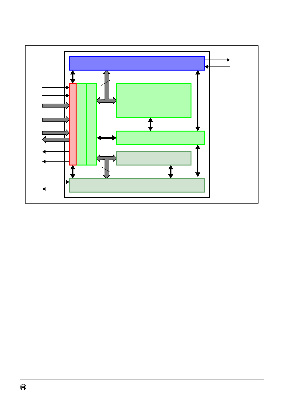
2.2 Block Diagram
Clock
Reset
Control
Address
DataIN
User’s Manual
CAN_Core
CAN-Message
Message RAM
(single ported)
Revision 1.6TTCAN
CAN_TX
CAN_RX
Message Handler
Trigger Memory
DataOUT
Wait
Interrupt
SWT, EVT
Module Interface
CPU IFC Register 2
CPU IFC Register 1
Trigger
TTCAN - Frame Synchronisation Entity
TMI
Figure 1: Block Diagram of the TTCAN
CAN_Core
CAN Protocol Controller and Rx/Tx Shift Register, handles all ISO 11898-1 protocol functions.
Message Handler
State Machine that controls the data transfer between the single ported Message RAM, the
CAN_Core’s Rx/Tx Shift Register, and the CPU IFC Registers. It also handles acceptance
filtering and the interrupt setting as programmed in the Control and Configuration Registers.
Message RAM / CPU IFC Registers
Single ported RAM, word-length = [CAN message & acceptance filter mask & control bits &
status bits]. To ensure data consistency, all CPU accesses to the Message RAM are relayed
through CPU IFC registers that have the same word-length as the Message RAM.
TTCAN
Frame Synchronisation Entity / Trigger Memory
manual_about.fm
State machine that controls the ISO 11898-4 time triggered communication. It synchronises
itself to the reference messages on the CAN bus, controls Cycle Time and Global Time, and
handles transmissions according to the predefined message schedule, the system matrix.
StopWatch Trigger, EVent Trigger, and Time Mark Interrupt are synchronisation interfaces.
The Trigger Memory stores the time marks of the system matrix that are linked to the
messages in the Message RAM.
Module Interface
Up to now the TTCAN module is provided with three different interfaces. An 8-bit interface for
the Motorola HC08 controller a 16-bit interface to the TI TMS470 controller, and two 16-bit
interfaces to the AMBA APB bus from ARM. They can easily be replaced by a user-defined
module interface.
BOSCH
-9/77-
11.11.02
Page 10

User’s Manual
Revision 1.6TTCAN
2.3 Operating Modes
2.3.1 Software Initialisation
The software initialization is started by setting the bit Init in the CAN Control Register, either
by software or by a hardware reset, or by going
Bus_Off
.
While Init is set, all message transfer from and to the CAN bus is stopped, the status of the
CAN bus output CAN_TX is
recessive
(HIGH). The counters of the EML are unchanged.
Setting Init does not change any configuration register.
To initialize the CAN Controller, the CPU has to set up the Bit Timing Register and each
Message Object. If a Message Object is not needed, it is sufficient to set it’s MsgVal bit to not
valid. Otherwise, the whole Message Object has to be initialized.
Access to the Bit Timing Register and to the BRP Extension Register for the configuration of
the bit timing and to the TT Operation Mode Register for the configuration of the time triggered
communication is enabled when both bits Init and CCE in the CAN Control Register are set.
Resetting Init (by CPU only) finishes the software initialisation. Afterwards the Bit Stream
Processor BSP (see section 4.2.1 on page 45) synchronizes itself to the data transfer on the
CAN bus by waiting for the occurrence of a sequence of 11 consecutive
) before it can take part in bus activities and starts the message transfer.
Idle
recessive
bits (≡
Bus
The initialization of the Message Objects is independent of Init and can be done anytime, but
the Message Objects should all be configured to particular identifiers or set to not valid before
the BSP starts the message transfer.
To change the configuration of a Message Object during normal operation, the CPU has to
start by setting MsgVal to not valid. When the configuration is completed, MsgVal is set to
valid again.
To change the configuration of the time triggered communication, the TTMode in the
TT Operation Mode Register must be set to Configuration Mode. Entering and leaving this
Configuration Mode requires that both bits Init and CCE are set.
2.3.2 CAN Message Transfer
Once the TTCAN is initialized and Init is reset to zero, the TTCAN’s CAN_Core synchronizes
itself to the CAN bus and starts the message transfer in the configured TTMode.
Received messages are stored into their appropriate Message Objects if they pass the
Message Handler’s acceptance filtering. The whole message including all arbitration bits, DLC
and eight data bytes is stored into the Message Object. If the Identifier Mask is used, the
arbitration bits which are masked to “don’t care” may be overwritten in the Message Object
manual_about.fm
when a received message is stored.
The CPU may read or write each message any time via the Interface Registers, the Message
Handler guarantees data consistency in case of concurrent accesses.
Messages to be transmitted are updated by the CPU. If a permanent Message Object
(arbitration and control bits set up during configuration) exists for the message, only the data
bytes are updated. How the transmission is started depends on the configured TTMode.If
several transmit messages are assigned to the same Message Object (when the number of
Message Objects is not sufficient), the whole Message Object has to be configured before the
transmission of this message is requested.
The transmission of any number of Message Objects may be requested at the same time, they
are transmitted subsequently according to their internal priority. Messages may be updated or
BOSCH
-10/77-
11.11.02
Page 11

User’s Manual
Revision 1.6TTCAN
set to not valid any time, even when their requested transmission is still pending. The old data
will be discarded when a message is updated before its pending transmission has started.
Depending on the configuration of the Message Object, the transmission of a message may
be requested autonomously by the reception of a remote frame with a matching identifier.
2.3.3 Disabled Automatic Retransmission
According to the CAN Specification (see ISO11898, 6.3.3 Recovery Management), the
TTCAN provides means for automatic retransmission of frames that have lost arbitration or
that have been disturbed by errors during transmission. The frame transmission service will
not be confirmed to the user before the transmission is successfully completed. By default,
this means for automatic retransmission is enabled. It can be disabled to enable the TTCAN to
work within a Time Triggered CAN (TTCAN, see ISO11898-1) environment.
The Disabled Automatic Retransmission mode is enabled by programming bit DAR in the CAN
one
Control Register to
. In this operation mode the programmer has to consider the different
behaviour of bits TxRqst and NewDat in the Control Registers of the Message Buffers:
•When a transmission starts bit TxRqst of the respective Message Buffer is reset, while bit
NewDat remains set.
•When the transmission completed successfully bit NewDat is reset.
When a transmission failed (lost arbitration or error) bit NewDat remains set. To restart the
transmission the CPU has to set TxRqst back to
Note :
It is not necessary to set DAR if the TTCAN is in time triggered operating mode.
2.3.4 Test Mode
The Test Mode is entered by setting bit Test in the CAN Control Register to
the bits Tx1, Tx0, LBack, Silent, NoRAM, and WdOff in the Test Register are writable. Bit Rx
monitors the state of pin CAN_RX and therefore is only readable. All Test Register functions
are disabled when bit Test is reset to zero.
Loop Back Mode, No Message RAM Mode, and CAN_TX Control Mode are hardware test
modes, not to be used by application programs.
Silent Mode and the Watchdog Disable Mode are software test modes.
2.3.4.1 Test Register (addresses 0x0B & 0x0A)
15 14 13 12 11 10 9 8 7 6 5 4 3 2 1 0
StW EvT res res res res res res Rx Tx1 Tx0 LBack Silent NoRAM res WdOff
rrrrrrrrrrwrwrwrwrwrrw
manual_about.fm
one
.
one
. In Test Mode
StW Monitors the actual value of the STOP_WATCH_TRIGGER pin
EvT Monitors the actual value of the EVENT_TRIGGER pin
Rx Monitors the actual value of the CAN_RX pin
one
zero
The CAN bus is recessive (CAN_RX = ‘1’).
The CAN bus is dominant (CAN_RX = ‘0’).
Tx1-0 Control of CAN_TX pin
00
01
10
11
BOSCH
Reset value, CAN_TX is controlled by the CAN_Core.
Sample Point can be monitored at CAN_TX pin.
CAN_TX pin drives a dominant (‘0’) value.
CAN_TX pin drives a recessive (‘1’) value.
-11/77-
11.11.02
Page 12
User’s Manual
Revision 1.6TTCAN
LBack Loop Back Mode
one
zero
Loop Back Mode is enabled.
Loop Back Mode is disabled.
Silent Silent Mode
one
zero
The module is in Silent Mode
Normal operation.
NoRAM No Message RAM Mode
one
zero
IF1 Registers used as Tx Buffer, IF2 Registers used as Rx Buffer.
No Message RAM Mode disabled, normal Message RAM usage.
WdOff Disable Watchdog
one
zero
The Watchdog disabled.
The Watchdog is enabled, after Initialization has finished (Init = 0).
Write access to the Test Register is enabled by setting bit Test in the CAN Control Register.
The different test functions may be combined, but Tx1-0 ≠ “00” disturbs message transfer.
2.3.4.2 Disable Watchdog Mode
The TT Application Watchdog (see chapter 3.5.6) can be disabled by programming the Test
Register bit WdOff to
one
and the Application_Watchdog_Limit AppWdL to 0x00. When bit
Test in the CAN Control Register is reset, WdOff is also reset if the TTCAN is in time triggered
operating mode; if the TTCAN is in event driven CAN mode, WdOff is remains set and the TT
Application Watchdog remains disabled (emulating the C_CAN function).
The TT Application Watchdog should not be disabled in a TTCAN application program.
2.3.4.3 Silent Mode
The CAN_Core can be set in Silent Mode by programming the Test Register bit Silent to
In Silent Mode, the TTCAN is able to receive valid data frames and valid remote frames, but it
sends only
is required to send a
internally so that the CAN_Core monitors this
recessive
in
affecting it by the transmission of
recessive
bits on the CAN bus and it cannot start a transmission. If the CAN_Core
dominant
bit (ACK bit, overload flag, active error flag), the bit is rerouted
dominant
bit, although the CAN bus may remain
state. The Silent Mode can be used to analyse the traffic on a CAN bus without
dominant
bits (Acknowledge Bits, Error Frames). Figure 2
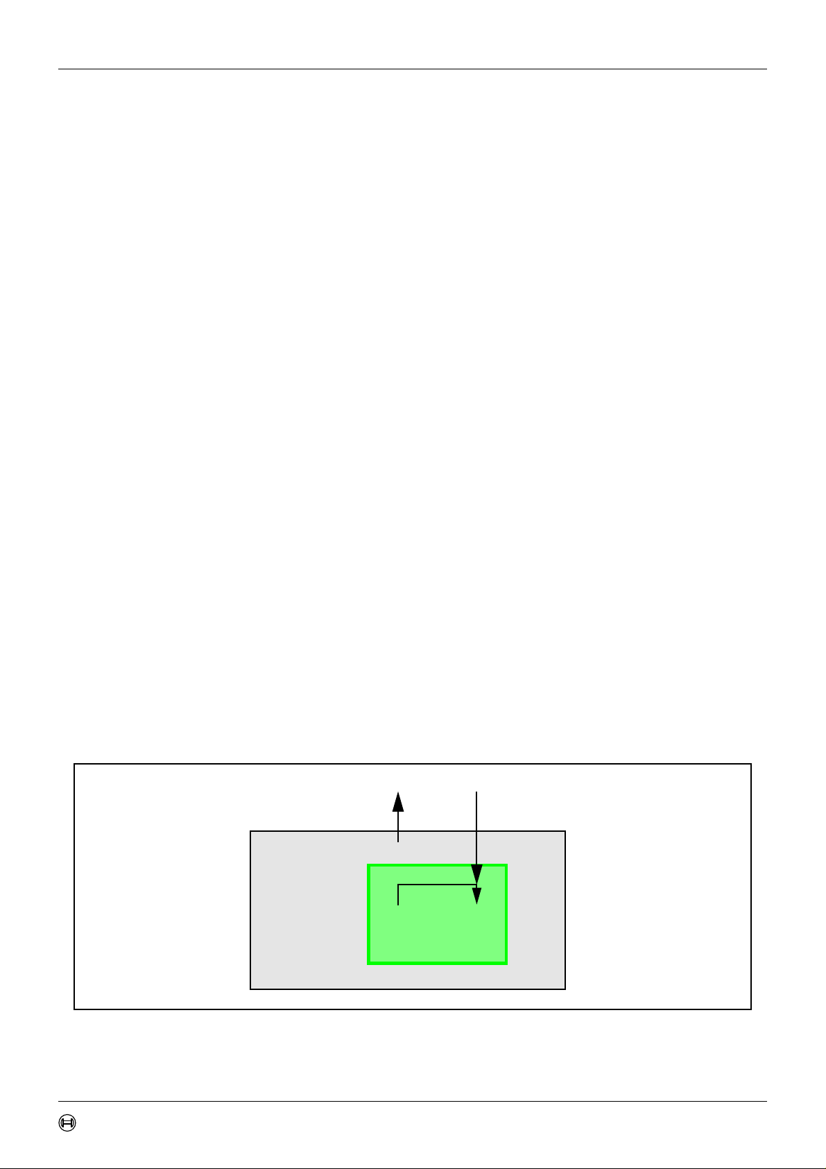
shows the connection of signals CAN_TX and CAN_RX to the CAN_Core in Silent Mode.
CAN_TX CAN_RX
manual_about.fm
TTCAN
=1
•
•
Tx Rx
one
.
CAN_Core
Figure 2: CAN_Core in Silent Mode
In ISO 11898-1, the Silent Mode is called the Bus Monitoring Mode.
BOSCH
-12/77-
11.11.02
Page 13
User’s Manual
Revision 1.6TTCAN
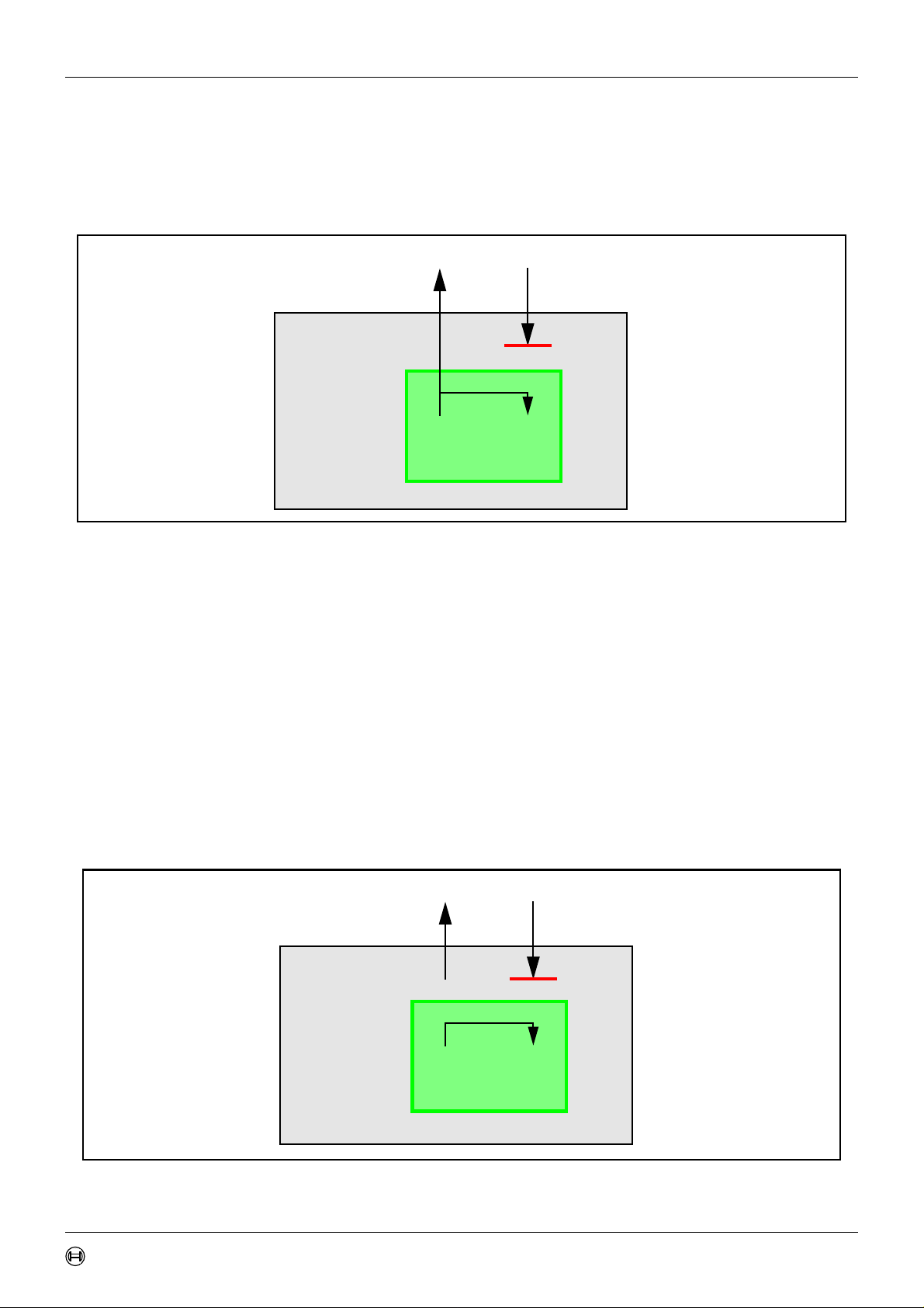
2.3.4.4 Loop Back Mode
The CAN_Core can be set in Loop Back Mode by programming the Test Register bit LBack to
one
. In Loop Back Mode, the CAN_Core treats its own transmitted messages as received
messages and stores them (if they pass acceptance filtering) into a Receive Buffer. Figure 3
shows the connection of signals CAN_TX and CAN_RX to the CAN_Core in Loop Back Mode.
CAN_TX CAN_RX
TTCAN
•
•
Tx Rx
CAN_Core
Figure 3: CAN_Core in Loop Back Mode
This mode is provided for hardware self-test functions. To be independent from external
stimulation, the CAN_Core ignores acknowledge errors (recessive bit sampled in the
acknowledge slot of a data/remote frame) in Loop Back Mode. In this mode the CAN_Core
performs an internal feedback from its Tx output to its Rx input. The actual value of the
CAN_RX input pin is disregarded by the CAN_Core. The transmitted messages can be
monitored at the CAN_TX pin.
2.3.4.5 Loop Back combined with Silent Mode
It is also possible to combine Loop Back Mode and Silent Mode by programming bits LBack
one
and Silent to
at the same time. This mode can be used for a “Hot Selftest”, meaning the
TTCAN hardware can be tested without affecting a running CAN system connected to the pins
CAN_TX and CAN_RX. In this mode the CAN_RX pin is disconnected from the CAN_Core
and the CAN_TX pin is held
recessive
. Figure 4 shows the connection of signals CAN_TX and
CAN_RX to the CAN_Core in case of the combination of Loop Back Mode with Silent Mode.
CAN_TX CAN_RX
manual_about.fm
TTCAN
=1
•
•
Tx Rx
CAN_Core
Figure 4: CAN_Core in Loop Back combined with Silent Mode
BOSCH
-13/77-
11.11.02
Page 14

User’s Manual
Revision 1.6TTCAN
2.3.4.6 Software control of Pin CAN_TX
Four output functions are available for the CAN transmit pin CAN_TX. Additionally to its
default function – the serial data output – it can drive the CAN Sample Point signal to monitor
the CAN_Core’sbit timing and it can drive constant dominant or recessive values.The last two
functions, combined with the readable CAN receive pin CAN_RX, can be used to check the
CAN bus’ physical layer.
The output mode of pin CAN_TX is selected by programming the Test Register bits Tx1 and
Tx0 as described in section 2.3.4.1 on page 11.
The three test functions for pin CAN_TX interfere with all CAN protocol functions. CAN_TX
must be left in its default function when CAN message transfer or any of the test modes Loop
Back Mode, Silent Mode, or No Message RAM Mode are selected.
2.3.4.7 No Message RAM Mode
The CAN_Core can be set in No Message RAM Mode by programming the Test Register bit
one
NoRAM to
. In this mode the TTCAN module operates without the Message RAM.
The IF1 Registers are used as Transmit Buffer. The transmission of the contents of the IF1
Registers is requested by writing the Busy bit of the IF1 Command Request Register to ‘1’.
The IF1 Registers are locked while the Busy bit is set. The Busy bit indicates that the
transmission is pending. The CPU-IFC’s output signal CAN_WAIT_B is disabled (always ‘1’)
in this mode.
As soon the CAN bus is idle, the IF1 Registers are loaded into the CAN_Core’s shift register
and the transmission is started. When the transmission has completed, the Busy bit is reset
and the locked IF1 Registers are released.
A pending transmission can be aborted at any time by resetting the Busy bit in the IF1
Command Request Register while the IF1 Registers are locked. If the CPU has reset the Busy
bit, a possible retransmission in case of lost arbitration or in case of an error is disabled.
The IF2 Registers are used as Receive Buffer. After the reception of a message the contents
of the shift register is stored into the IF2 Registers, without any acceptance filtering.
Additionally, the actual contents of the shift register can be monitored during the message
transfer. Each time a read Message Object is initiated by writing the Busy bit of the IF2
Command Request Register to ‘1’, the contents of the shift register is stored into the IF2
Registers.
In No Message RAM Mode the evaluationof all Message Object related control and status bits
and of the control bits of the IFx Command Mask Registers is turned off. The message
number of the Command request registers is not evaluated. The NewDat and MsgLst bits of
the IF2 Message Control Register retain their function, DLC3-0 will show the received DLC,
manual_about.fm
the other control bits will be read as ‘0’.
The No Message RAM Mode is a hardware test mode that allows to evaluate the TTCAN IP
RTL code in FPGA types that do not support the TTCAN’s Message RAM structure.
BOSCH
-14/77-
11.11.02
Page 15

User’s Manual
Revision 1.6TTCAN
3. Programmer’s Model
The TTCAN module allocates an address space of 256 bytes. The registers are organized as
16-bit registers, with the high byte at the odd address and the low byte at the even address.
The two sets of interface registers (IF1 and IF2) control the CPU access to the Message RAM.
They buffer the data to be transferred to and from the RAM, avoiding conflicts between CPU
accesses and message reception/transmission.
Address Name Reset Value Note
CAN Base+0x00 CAN Control Register 0x0001 CAN config register
CAN Base+0x02 Status Register 0x0000 CAN status register
CAN Base+0x04 Error Counter 0x0000 CAN status register
CAN Base+0x06 Bit Timing Register 0x2301 CAN config reg., req. CCE
CAN Base+0x08 Interrupt Register 0x0000 CAN status register
CAN Base+0x0A Test Register 0x00& 0br0000000
CAN Base+0x0C BRP Extension Register 0x0000 CAN config reg., req. CCE
CAN Base+0x0E Trigger Memory Access 0x0000 TTCAN config register
CAN Base+0x10 IF1 Command Request 0x0001 CAN appl. IF1 Register Set
CAN Base+0x12 IF1 Command Mask 0x0000
CAN Base+0x14 IF1 Mask 1 0xFFFF
CAN Base+0x16 IF1 Mask 2 0xFFFF
CAN Base+0x18 IF1 Arbitration 1 0x0000
CAN Base+0x1A IF1 Arbitration2 0x0000
CAN Base+0x1C IF1 Message Control 0x0000
CAN Base+0x1E IF1 Data A 1 0x0000
CAN Base+0x20 IF1 Data A 2 0x0000
CAN Base+0x22 IF1 Data B 1 0x0000
CAN Base+0x24 IF1 Data B 2 0x0000
CAN Base+0x26 — reserved —
CAN Base+0x28 TT Operation Mode 0x0000 TTCAN config register
CAN Base+0x2A TT Matrix Limits1 0x0000 TTCAN config register
CAN Base+0x2C TT Matrix Limits2 0x0000 TTCAN config register
CAN Base+0x2E TT Application Watchdog 0x0001 TTCAN config register
CAN Base+0x30 TT Interrupt Enable 0x0000 TTCAN appl. register
CAN Base+0x32 TT Interrupt Vector 0x0000 TTCAN status register
CAN Base+0x34 TT Global Time 0x0000 TTCAN status register
manual_about.fm
CAN Base+0x36 TT Cycle Time 0x0000 TTCAN status register
CAN Base+0x38 TT Local Time 0x0000 TTCAN status register
CAN Base+0x3A TT Master State 0x0000 TTCAN status register
CAN Base+0x3C TT Cycle Count 0x003F TTCAN status register
CAN Base+0x3E TT Error Level 0x0000 TTCAN status register
CAN Base+0x40 IF2 Command Request 0x0001 CAN appl. IF2 Register Set
CAN Base+0x42 IF2 Command Mask 0x0000
CAN Base+0x44 IF2 Mask 1 0xFFFF
CAN Base+0x46 IF2 Mask 2 0xFFFF
1)
r signifies the actual value of the CAN_RX pin.
2)
Reserved bits are read as ’0’ except for IFx Mask 2 Register where they are read as ’1’
2)
1)
CAN appl. reg., req. Test
BOSCH
-15/77-
11.11.02
Page 16

User’s Manual
Address Name Reset Value Note
CAN Base+0x48 IF2 Arbitration 1 0x0000 CAN appl. IF2 Register Set
CAN Base+0x4A IF2 Arbitration 2 0x0000
CAN Base+0x4C IF2 Message Control 0x0000
CAN Base+0x4E IF2 Data A 1 0x0000
CAN Base+0x50 IF2 Data A 2 0x0000
CAN Base+0x52 IF2 Data B 1 0x0000
CAN Base+0x54 IF2 Data B 2 0x0000
CAN Base+0x56 TUR-NumeratorCfg 0x0000 TTCAN config register
CAN Base+0x58 TUR-DenominatorCfg 0x1000 TTCAN config register
CAN Base+0x5A TUR-NumeratorActL 0x0000 TTCAN status register
CAN Base+0x5C TUR-NumeratorActH 0x0001 TTCAN status register
CAN Base+0x5E — reserved —
CAN Base+0x60 Stop_Watch 0x0000 TTCAN status register
CAN Base+0x62 — reserved —
CAN Base+0x64 Global Time Preset 0x0000 TTCAN appl. register
CAN Base+0x66 Clock Control 0x1000 TTCAN appl. register
CAN Base+0x68 Sync_Mark 0x0000 TTCAN status register
CAN Base+0x6A — reserved —
CAN Base+0x6C Time Mark 0x0000 TTCAN appl. register
CAN Base+0x6E Gap Control 0x0000 TTCAN appl. register
CAN Base+0x70-0x7E — reserved —
CAN Base+0x80 Transmission Request 1 0x0000 CAN status register
CAN Base+0x82 Transmission Request 2 0x0000 CAN status register
CAN Base+0x84-0x8E — reserved —
CAN Base+0x90 New Data 1 0x0000 CAN status register
CAN Base+0x92 New Data 2 0x0000 CAN status register
CAN Base+0x94-0x9E — reserved —
CAN Base+0xA0 Interrupt Pending 1 0x0000 CAN status register
CAN Base+0xA2 Interrupt Pending 2 0x0000 CAN status register
CAN Base+0xA4-0xAE — reserved —
CAN Base+0xB0 Message Valid 1 0x0000 CAN status register
CAN Base+0xB2 Message Valid 2 0x0000 CAN status register
CAN Base+0xB4-0xBE — reserved —
1)
r signifies the actual value of the CAN_RX pin.
2)
Reserved bits are read as ’0’ except for IFx Mask 2 Register where they are read as ’1’
manual_about.fm
2)
2)
2)
2)
2)
2)
2)
2)
Revision 1.6TTCAN
Figure 5: TTCAN Register Summary
3.1 Hardware Reset Description
After hardware reset, the registers of the TTCAN hold the values described in figure 5.
Additionally the
Bus_Off
state is reset and the output CAN_TX is set to
recessive
(HIGH). The
value 0x0001 (Init = ‘1’) in the CAN Control Register enables the software initialisation. The
TTCAN does not influence the CAN bus until the CPU resets Init to ‘0’.
The data in the Message RAM is (apart from the MsgVal, NewDat, TxRqst, and IntPnd bits)
RAM
notaffectedbyahardwarereset.Afterpower-on,thecontentsofthe Message
BOSCH
-16/77-
is undefined.
11.11.02
Page 17

User’s Manual
Revision 1.6TTCAN
3.2 CAN Protocol Related Registers
These registers are related to the CAN protocol controller in the CAN Core. They control the
operating modes and the configuration of the CAN bit timing and provide status information.
3.2.1 CAN Control Register (addresses 0x01 & 0x00)
1514131211109876543210
res res res res res res res res Test CCE DAR res EIE SIE IE Init
rrrrrrrrrwrwrwrrwrwrwrw
Test Test Mode Enable
one
zero
Test Mode.
Normal Operation.
CCE Configuration Change Enable
one
zero
The CPU has write access to the configuration registers (while Init =
The CPU has no write access to the configuration registers.
one
DAR Disable Automatic Retransmission
one
zero
Automatic Retransmission disabled.
Automatic Retransmission of not successful messages enabled.
).
EIE Error Interrupt Enable
one
Enabled - A change in the bits BOff or EWarn in the Status Register will
generate an interrupt.
zero
Disabled - No Error Status Interrupt will be generated.
SIE Status Change Interrupt Enable
one
Enabled - An interrupt will be generated when a message transfer is successfully completed or a CAN bus error is detected.
zero
Disabled - No Status Change Interrupt will be generated.
IE Module Interrupt Enable
one
Enabled - Interrupts will set IRQ_B to LOW. IRQ_B remains LOW until all
pending interrupts are processed.
zero
Disabled - Module Interrupt IRQ_B is always HIGH.
Init Initialization
one
zero
Initialization is started.
Normal Operation.
The configuration registers controlled by CCE are the Bit Timing Register, the BRP Extension
manual_about.fm
Register, and the TT Operation Mode Register.
Note :
The
Bus_Off
ting or resetting Init. If the device goes
activities. Once Init has been cleared by the CPU, the device will then wait for 129 occurrences
of
Bus Idle
of the Bus_Off recovery sequence, the Error Management Counters will be reset.
recovery sequence (see CAN Specification Rev. 2.0) cannot be shortened by set-
(129 * 11 consecutive
Bus_Off
recessive
, it will set Init of its own accord, stopping all bus
bits) before resuming normal operations. At the end
During the waiting time after the resetting of Init, each time a sequence of 11
recessive
bits
has been monitored, a Bit0Error code is written to the Status Register, enabling the CPU to
readily check up whether the CAN bus is stuck at
dominant
or continuously disturbed and to
monitor the proceeding of the Bus_Off recovery sequence.
BOSCH
-17/77-
11.11.02
Page 18

User’s Manual
Revision 1.6TTCAN
3.2.2 Status Register (addresses 0x03 & 0x02)
1514131211109876543210
res res res res res res res res BOff
rrrrrrrrrrrrwrw rw
EWarn
EPass RxOk TxOk LEC
BOff Bus_Off Status
one
zero
The CAN module is in Bus_Off state.
The CAN module is not Bus_Off.
EWarn Warning Status
one
At least one of the error counters in the EML has reached the error warning
limit of 96.
zero
Both error counters are below the error warning limit of 96.
EPass Error Passive
one
zero
The CAN Core is in the
The CAN Core is
error active
error passive
.
state as defined in the CAN Specification.
RxOk Received a Message Successfully
one
Since this bit was last reset (to zero) by the CPU, a message has been successfully received (independent of the result of acceptance filtering).
zero
Since this bit was last reset by the CPU, no message has been successfully
received. This bit is never reset by the CAN Core.
TxOk Transmitted a Message Successfully
one
Since this bit was last reset by the CPU, a message has been successfully
(error free and acknowledged by at least one other node) transmitted.
zero
Since this bit was reset by the CPU, no message has been successfully transmitted. This bit is never reset by the CAN Core.
LEC Last Error Code (Type of the last error to occur on the CAN bus)
0 No Error
1
Stuff Error : More than 5 equal bits in a sequence have occurred in a part of a
received message where this is not allowed.
2
3
Form Error : A fixed format part of a received frame has the wrong format.
AckError : The message this CAN Core transmitted was not acknowledged by
another node.
manual_about.fm
4
5
Bit1Error : During the transmission of a message (with the exception of the
arbitration field), the device wanted to send a
‘1’), but the monitored bus value was
dominant
recessive
.
Bit0Error : During the transmission of a message (or acknowledge bit, or
active error flag, or overload flag), the device wanted to send a
(data or identifier bit logical value ‘0’), but the monitored bus value was
. During
sive
recessive
Bus_Off
recovery this status is set each time a sequence of 11
bits has been monitored. This enables the CPU to monitor the pro-
ceeding of the Bus_Off recovery sequence (indicating the bus is not stuck at
dominant
6
CRCError : The CRC check sum was incorrect in the message received, the
or continuously disturbed).
CRC received for an incoming message does not match with the calculated
CRC for the received data.
7 unused : When the LEC shows the value ‘7’, no CAN bus event was detected
since the CPU wrote this value to the LEC.
level(bit of logical value
dominant
level
reces-
BOSCH
-18/77-
11.11.02
Page 19

User’s Manual
Revision 1.6TTCAN
The LEC field holds a code which indicates the type of the last error to occur on the CAN bus.
This field will be cleared to ‘0’ when a message has been transferred (reception or transmission) without error. The unused code ‘7’ may be written by the CPU to check for updates.
3.2.2.1 Status Interrupts A Status Interrupt is generated by bits BOff and EWarn (Error Interrupt, EIE)orbyRxOk,
TxOk, and LEC (Status Change Interrupt, SIE) assumed that the corresponding enable bits in
the CAN Control Register are set. A change of bit EPass or a CPU write to RxOk, TxOk,or
LEC will never generate a Status Interrupt.
When SIE is set, a Status Interrupt will be generated at each CAN bus error and at each valid
CAN message, independent of the Message RAM configuration.
Reading the Status Register will clear the Status Interrupt value (8000h) in the Interrupt
Register, if it is pending.
3.2.3 Error Counter (addresses 0x05 & 0x04)
1514131211109876543210
RP REC6-0 TEC7-0
rr r
RP Receive Error Passive
one
The Receive Error Counter has reached the
error passive
level as defined
in the CAN Specification.
zero
The Receive Error Counter is below the
error passive
level.
REC6-0 Receive Error Counter
Actual state of the Receive Error Counter. Values between 0 and 127.
TEC7-0 Transmit Error Counter
Actual state of the Transmit Error Counter. Values between 0 and 255.
3.2.4 Bit Timing Register (addresses 0x07 & 0x06)
1514131211109876543210
res TSeg2 TSeg1 SJW BRP
rrw rw rw rw
TSeg1 The time segment before the sample point
0x01-0x0F
manual_about.fm
valid values for TSeg1 are [1 … 15]. The actual interpretation by
the hardware of this value is such that one more than the value
programmed here is used.
TSeg2 The time segment after the sample point
0x0-0x7
valid values for TSeg2 are [0 … 7]. The actual interpretation by
the hardware of this value is such that one more than the value
programmed here is used.
SJW (Re)Synchronisation Jump Width
0x0-0x3
Valid programmed values are 0-3. The actual interpretation by
the hardware of this value is such that one more than the value
programmed here is used.
BOSCH
-19/77-
11.11.02
Page 20

User’s Manual
Revision 1.6TTCAN
BRP Baud Rate Prescaler
0x00-0x3F
The value by which the oscillator frequency is divided for generating the bit time quanta. The bit time is built up from a multiple
of this quanta. Valid values for the Baud Rate Prescaler are
[0 … 63]. The actual interpretation by the hardware of this value
is such that one more than the value programmed here is used.
This register is only writable if bits CCE and Init in the CAN Control Register are set. The CAN
bit time may be programed in the range of [4 … 25] time quanta. The CAN time quantum may
be programmed in the range of [1 … 1024] CAN_CLK periods. For details see chapter 4.2.1.
Note :
With a module clock CAN_CLK of 8 MHz and BRPE = 0x00, the reset value of 0x2301 configures the TTCAN for a bit rate of 500 kBit/s.
3.2.5 BRP Extension Register (addresses 0x0D & 0x0C)
1514131211109876543210
res res res res res res res res res res res res BRPE
rrrrrrrrrrrr rw
BRPE Baud Rate Prescaler Extension
0x00-0x0F By programming BRPE the Baud Rate Prescaler can be
extended to values up to 1023. The actual interpretation by the
hardware is that one more than the value programmed by BRPE
(MSBs) and BRP (LSBs) is used.
This register is only writable if bits CCE and Init in the CAN Control Register are set.
Note :
The width of BRPE may be increased to more than its default width of 4 bits in particular implementations of the TTCAN IP module width a high module clock frequency.
3.3 Message Interface Register Sets
Address IF1 Register Set Address IF2 Register Set
CAN Base+0x10 IF1 Command Request CAN Base+0x40 IF2 Command Request
CAN Base+0x12 IF1 Command Mask CAN Base+0x42 IF2 Command Mask
CAN Base+0x14 IF1 Mask 1 CAN Base+0x44 IF2 Mask 1
CAN Base+0x16 IF1 Mask 2 CAN Base+0x46 IF2 Mask 2
CAN Base+0x18 IF1 Arbitration 1 CAN Base+0x48 IF2 Arbitration 1
CAN Base+0x1A IF1 Arbitration 2 CAN Base+0x4A IF2 Arbitration 2
CAN Base+0x1C IF1 Message Control CAN Base+0x4C IF2 Message Control
manual_about.fm
CAN Base+0x1E IF1 Data A 1 CAN Base+0x4E IF2 Data A 1
CAN Base+0x20 IF1 Data A 2 CAN Base+0x50 IF2 Data A 2
CAN Base+0x22 IF1 Data B 1 CAN Base+0x52 IF2 Data B 1
CAN Base+0x24 IF1 Data B 2 CAN Base+0x54 IF2 Data B 2
Figure 6: IF1 and IF2 Message Interface Register Sets
There are two sets of Interface Registers that control the CPU access to the Message RAM.
The Interface Registers avoid (by buffering the data to be transferred) conflicts between CPU
access to the Message RAM and CAN message reception and transmission. A complete
Message Object (see chapter 3.3.4) or parts of the Message Object may be transferred
between the Message RAM and the IFx Message Buffer registers (see chapter 3.3.3) in one
BOSCH
-20/77-
11.11.02
Page 21

User’s Manual
Revision 1.6TTCAN
single transfer. This transfer,performed in parallel on all selected parts of the Message Object,
guarantees the data consistency of the CAN message. Figure 6 shows the structure of the two
Interface Register sets.
The function of the two Interface Register sets is identical (except for test mode NoRAM). The
second interface register set is provided to serve application programming. Two groups of
software drivers may defined, each group is restricted to the use of one of the Interface
Register sets. The software drivers of one group may interrupt software drivers of the other
group, but not of the same group.
In a simple example, there is one Read_Message task that uses IFC1 to get received
messages from the Message RAM and there is one Write_Message task that uses IFC2 to
write messages to be transmitted into the Message RAM. Both tasks may interrupt each other.
Each set of Interface Registers consists of Message Buffer Registers controlled by their own
Command Registers. The Command Mask Register specifies the direction of the data transfer
and which parts of a Message Object will be transferred. The Command Request Register is
used to select a Message Object in the Message RAM as target or source for the transfer and
to start the action specified in the Command Mask Register.
3.3.1 IFx Command Mask Registers
The control bits of the IFx Command Mask Register specify the transfer direction and select
which of the IFx Message Buffer Registers are source or target of the data transfer.
15 14 13 12 11 10 9 8 7 6 5 4 3 2 1 0
IF1 CommandMask Register
(addresses 0x13 & 0x12)
IF2 CommandMask Register
(addresses 0x43 & 0x42)
res WR/RD Mask Arb Control
res WR/RD Mask Arb Control
r r r r r r r r rw rw rw rw rw rw rw rw
ClrIntPnd
ClrIntPnd
TxRqst/
NewDat
TxRqst/
NewDat
Data A Data B
Data A Data B
WR/RD Write / Read
one
Write: Transfer data from the selected Message Buffer Registers to the
Message Object addressed by the Command Request Register.
zero
Read: Transfer data from the Message Object addressed by the Command Request Register into the selected Message Buffer Registers.
The other bits of IFx Command Mask Register have different functions depending on the
transfer direction :
3.3.1.1 Direction = Write Mask Access Mask Bits
manual_about.fm
one
zero
transfer Identifier Mask + MDir + MXtd to Message Object.
Mask bits unchanged.
Arb Access Arbitration Bits
one
zero
transfer Identifier + Dir + Xtd + MsgVal to Message Object.
Arbitration bits unchanged.
Control Access Control Bits
Note :
BOSCH
one
zero
MSC2-0 is read-only in time triggered operating mode.
transfer Control Bits to Message Object.
Control Bits unchanged.
-21/77-
11.11.02
Page 22

User’s Manual
ClrIntPnd Clear Interrupt Pending Bit
Note :
When writing to a Message Object, this bit is ignored.
TxRqst/NewDatAccess Transmission Request Bit
Note :
one
zero
If a transmission is requested by setting TxRqst/NewDat in the IFx Command Mask Register,
bit TxRqst in the IFx Message Control Register will be ignored.
set TxRqst bit
TxRqst bit unchanged
Data A Access Data Bytes 0-3
one
zero
transfer Data Bytes 0-3 to Message Object.
Data Bytes 0-3 unchanged.
Data B Access Data Bytes 4-7
one
zero
transfer Data Bytes 4-7 to Message Object.
Data Bytes 4-7 unchanged.
3.3.1.2 Direction = Read Mask Access Mask Bits
one
zero
transfer Identifier Mask + MDir + MXtd to IFx Message Buffer Register.
Mask bits unchanged.
Revision 1.6TTCAN
Arb Access Arbitration Bits
one
zero
transfer Identifier + Dir + Xtd + MsgVal to IFx Message Buffer Register.
Arbitration bits unchanged.
Control Access Control Bits
one
zero
transfer Control Bits to IFx Message Buffer Register.
Control Bits unchanged.
ClrIntPnd Clear Interrupt Pending Bit
one
zero
clear IntPnd bit in the Message Object.
IntPnd bit remains unchanged.
TxRqst/NewDatAccess New Data Bit
Note :
one
zero
A read access to a Message Object can be combined with the reset of the control bits IntPnd
and NewDat. The values of these bits transferred to the IFx Message Control Register always
reflect the status before resetting them.
clear NewDat bit in the Message Object.
NewDat bit remains unchanged.
Data A Access Data Bytes 0-3
manual_about.fm
one
zero
transfer Data Bytes 0-3 to IFx Message Buffer Register.
Data Bytes 0-3 unchanged.
Data B Access Data Bytes 4-7
Note :
one
zero
The speed of the message transfer does not depend on how many bytes are transferred.
transfer Data Bytes 4-7 to IFx Message Buffer Register.
Data Bytes 4-7 unchanged.
3.3.2 IFx Command Request Registers
A message transfer is started as soon as the CPU has written the message number to low
byte of the Command Request Register. With this write operation, the Busy bit is
automatically set to ‘1’ to notify the CPU that a transfer is in progress. After a wait time of 3 to
BOSCH
-22/77-
11.11.02
Page 23

User’s Manual
Revision 1.6TTCAN
6 CAN_CLK periods, the transfer between the Interface Register and the Message RAM has
completed and the Busy bit is cleared to ‘0’. The upper limit of the wait time occurs when the
message transfer coincides with a CAN message transmission, acceptance filtering, or
message storage. If the CPU-IFC is implemented with the wait-function, the CPU is halted
while the Busy bit is set. If the CPU writes to both Command Request Registers consecutively
(requests a second transfer while another transfer is already in progress), the second transfer
starts when the first one is completed.
IF1 Command Request Register
(addresses 0x11 & 0x10)
IF2 Command Request Register
(addresses 0x41 & 0x40)
1514131211109876543210
Busy res res Message Number
Busy res res Message Number
rr rrw
Busy Busy Flag
one
zero
set to one when writing to the IFx Command Request Register
reset to zero when read/write action has finished.
Message Number
0x01-0x20
Valid Message Number, the Message Object in the Message
RAM is selected for data transfer.
Note :
0x00
0x21-0x3F
When an invalid Message Number is written to the Command Request Register, the Message
Number will be transformed into a valid value and that Message Object will be transferred.
Not a valid Message Number, interpreted as
Not a valid Message Number, interpreted as
0x20
.
0x01-0x1F
.
3.3.3 IFx Message Buffer Registers
The bits of the Message Buffer registers mirror the Message Objects in the Message RAM.
The function of the Message Objects bits is described in chapter 3.3.4.
3.3.3.1 IFx Mask Registers
IF1 Mask 1 Register
(addresses 0x15 & 0x14)
IF1 Mask 2 Register
(addresses 0x17 & 0x16)
IF2 Mask 1 Register
(addresses 0x45 & 0x44)
IF2 Mask 2 Register
(addresses 0x47 & 0x46)
manual_about.fm
3.3.3.2 IFx Arbitration Registers
IF1 Arbitration 1 Register
(addresses 0x19 & 0x18)
IF1 Arbitration 2 Register
(addresses 0x1B& 0x1A)
IF2 Arbitration 1 Register
(addresses 0x49 & 0x48)
IF2 Arbitration 2 Register
(addresses 0x4B & 0x4A)
15 14 131211109876543210
Msk15-0
MXtd MDir res Msk28-16
Msk15-0
MXtd MDir res Msk28-16
rw rw r rw
15 14 131211109876543210
ID15-0
MsgVal Xtd Dir ID28-16
ID15-0
MsgVal Xtd Dir ID28-16
rw rw rw rw
BOSCH
-23/77-
11.11.02
Page 24

User’s Manual
3.3.3.3 IFx Message Control Registers
Revision 1.6TTCAN
IF1MessageControl Register
(addresses 0x1D & 0x1C)
IF2MessageControl Register
(addresses 0x4D & 0x4C)
15 14 13 12 11 10 9 8 7 6 5 4 3 2 1 0
NewDat MsgLst IntPnd UMask TxIE RxIE RmtEn TxRqst EoB MSC2-0 DLC3-0
NewDat MsgLst IntPnd UMask TxIE RxIE RmtEn TxRqst EoB MSC2-0 DLC3-0
rw rw rw rw rw rw rw rw rw rw rw
3.3.3.4 IFx Data A and Data B Registers
The data bytes of CAN messages are stored in the IFx registers in the following order:
15 14 13 12 11 10 9 8 7 6 5 4 3 2 1 0
IF1 Message Data A1 (addresses 0x1F & 0x1E) Data(1) Data(0)
IF1 Message Data A2 (addresses 0x21 & 0x20) Data(3) Data(2)
IF1 Message Data B1 (addresses 0x23 & 0x22) Data(5) Data(4)
IF1 Message Data B2 (addresses 0x25 & 0x24) Data(7) Data(6)
IF2 Message Data A1 (addresses 0x4F & 0x4E) Data(1) Data(0)
IF2 Message Data A2 (addresses 0x51 & 0x50) Data(3) Data(2)
IF2 Message Data B1 (addresses 0x53 & 0x52) Data(5) Data(4)
IF2 Message Data B2 (addresses 0x55 & 0x54) Data(7) Data(6)
rw rw
In a CAN Data Frame, Data(0) is the first, Data(7) is the last byte to be transmitted or received.
In CAN’s serial bit stream, the MSB of each byte will be transmitted first.
3.3.4 Message Object in the Message Memory
There are 32 Message Objects in the Message RAM. To avoid conflicts between CPU access
to the Message RAM and CAN message reception and transmission, the CPU cannot directly
access the Message Objects, these accesses are handled via the IFx Interface Registers.
Figure 7 gives an overview of the two structure of a Message Object.
Message Object
UMask Msk28-0 MXtd MDir EoB MSC2-0 NewDat MsgLst RxIE TxIE IntPnd RmtEn TxRqst
MsgVal ID28-0 Xtd Dir DLC3-0 Data 0 Data 1 Data 2 Data 3 Data 4 Data 5 Data 6 Data 7
Figure 7: Structure of a Message Object in the Message Memory
MsgVal Message Valid
manual_about.fm
Note :
one
zero
The CPU must reset the MsgVal bit of all unused Messages Objects during the initialization
before it resets bit Init in the CAN Control Register. This bit must also be reset before the identifier Id28-0, the control bits Xtd, Dir, or the Data Length Code DLC3-0 are modified, or if the
Messages Object is no longer required.
The Message Object is configured and should be considered by the Message Handler.
The Message Object is ignored by the Message Handler.
UMask Use Acceptance Mask
Note :
one
zero
If the UMask bit is set to
initialization of the Message Object before MsgVal is set to
Use Mask (Msk28-0, MXtd, and MDir) for acceptance filtering
Mask ignored.
one
, the Message Object’s mask bits have to be programmed during
one
.
BOSCH
-24/77-
11.11.02
Page 25

ID28-0 Message Identifier
ID28 - ID0 29-bit Identifier (“Extended Frame”).
ID28 - ID18 11-bit Identifier (“Standard Frame”).
Msk28-0 Identifier Mask
one
zero
The corresponding identifier bit is used for acceptance filtering.
The corresponding bit in the identifier of the message object cannot inhibit
the match in the acceptance filtering.
Xtd Extended Identifier
one
zero
The 29-bit (“extended”) Identifier will be used for this Message Object.
The 11-bit (“standard”) Identifier will be used for this Message Object.
MXtd Mask Extended Identifier
Note :
one
zero
When 11-bit (“standard”) Identifiers are used for a Message Object, the identifiers of received
Data Frames are written into bits ID28 to ID18. For acceptance filtering, only these bits together
with mask bits Msk28 to Msk18 are considered.
The extended identifier bit (IDE) is used for acceptance filtering.
The extended identifier bit (IDE) has no effect on the acceptance filtering
Dir Message Direction
one
Direction =
transmit
mitted as a Data Frame. On reception of a Remote Frame with matching
identifier, the TxRqst bit of this Message Object is set (if RmtEn =
zero
Direction =
receive
Message Object is transmitted. On reception of a Data Frame with matching identifier, that message is stored in this Message Object.
User’s Manual
Revision 1.6TTCAN
:OnTxRqst, the respective Message Object is trans-
one
).
:OnTxRqst, a Remote Frame with the identifier of this
MDir Mask Message Direction
one
zero
The message direction bit (Dir) is used for acceptance filtering.
The message direction bit (Dir) has no effect on the acceptance filtering.
The Arbitration Registers ID28-0, Xtd, and Dir are used to define the identifier and type of
outgoing messages and are used (together with the mask registers Msk28-0, MXtd, and
MDir) for acceptance filtering of incoming messages. A received message is stored into the
valid Message Object with matching identifier and Direction=
Direction=
with Xtd =
transmit
one
(Remote Frame). Extended frames can be stored only in Message Objects
, standard frames in Message Objects with Xtd =
receive
zero
. If a received message
(Data Frame) or
(Data Frameor Remote Frame)matches with more than one valid Message Object, it is stored
into that with the lowest message number. For details see chapter 4.1.3 Acceptance Filtering
of Received Messages.
EoB End of Block
manual_about.fm
one
zero
Single Message Object or last Message Object of a FIFO Buffer Block.
Message Object belongs to a FIFO Buffer Block and is not the last Mes-
sage Object of that FIFO Buffer Block.
Note :
This bit is used to concatenate two ore more Message Objects (up to 32) to build a FIFO Buffer.
For single Message Objects (not belonging to a FIFO Buffer) this bit must always be set
to one. For details on the concatenation of Message Objects see chapter 4.2.2.3.
MSC2-0 Message Status Count
Note :
0-7
The Message Status Count is status information that is generated for periodic Message Objects
in Time Triggered Communication (ISO11898-4). It has no function in Event Driven CAN Communication (ISO11898-1) and for arbitrating Message Objects in TTCAN.
The actual value of the Message Status Count, read-only in active mode.
BOSCH
-25/77-
11.11.02
Page 26

NewDat New Data
one
The Message Handler or the CPU has written new data into the data portion of this Message Object.
zero
No new data has been written into the data portion of this Message Object
by the Message Handler since last time this flag was cleared by the CPU.
User’s Manual
Revision 1.6TTCAN
MsgLst Message Lost (only valid for Message Objects with direction =
one
The Message Handler stored a new message into this object when New-
Dat was still set, the CPU has lost a message.
zero
No message lost since last time this bit was reset by the CPU.
RxIE Receive Interrupt Enable
one
zero
IntPnd will be set after a successful reception of a frame.
IntPnd will be left unchanged after a successful reception of a frame.
TxIE Transmit Interrupt Enable
one
zero
IntPnd will be set after a successful transmission of a frame.
IntPnd
will be
left unchanged after the successful transmission of a frame.
IntPnd Interrupt Pending
one
This message object is the source of an interrupt. The Interrupt Identifier
in the Interrupt Register will point to this message object if there is no
other interrupt source with higher priority.
zero
This message object is not the source of an interrupt.
RmtEn Remote Enable
one
zero
At the reception of a Remote Frame, TxRqst is set.
At the reception of a Remote Frame, TxRqst is left unchanged.
TxRqst Transmit Request
Note :
one
zero
In TTCAN mode, there are two types of transmit Message Objects. When NewDat is set and
TxRqst is reset, the message will be transmitted periodically at each Transmit_Trigger for this
message, without changing NewDat or TxRqst. When both NewDat and TxRqst are set, the
message will be transmitted once at a Transmit_Trigger for this message, inside an arbitrating
time window. When the transmission was not successful, it will be repeated at the next
Transmit_Trigger for this message. When the transmission was successful, NewDat is reset.
The transmission of this Message Object is requested and is not yet done.
This Message Object is not waiting for transmission.
receive
)
DLC3-0 Data Length Code
manual_about.fm
Note :
BOSCH
0-8
9-15
The Data Length Code of a Message Object must be defined the same as in all the corresponding objects with the same identifier at other nodes. When the Message Handler stores a data
frame, it will write the DLC to the value given by the received message.
Data Frame has 0-8 data bytes.
Data Frame has 8 data bytes
-26/77-
11.11.02
Page 27

User’s Manual
Revision 1.6TTCAN
Data 0 1st data byte of a CAN Data Frame
Data 1 2nd data byte of a CAN Data Frame
Data 2 3rd data byte of a CAN Data Frame
Data 3 4th data byte of a CAN Data Frame
Data 4 5th data byte of a CAN Data Frame
Data 5 6th data byte of a CAN Data Frame
Data 6 7th data byte of a CAN Data Frame
Data 7 8th data byte of a CAN Data Frame
Note :
Byte Data 0 is the first data byte shifted into the shift register of the CAN Core during a reception, byte Data 7 is the last. When the Message Handler stores a Data Frame, it will write all the
eight data bytes into a Message Object. If the Data Length Code is less than 8, the remaining
bytes of the Message Object will be overwritten by non specified values.
3.4 Message Handler Registers All Message Handler registers are read-only. Their contents (TxRqst, NewDat, IntPnd, and
MsgVal bits of each Message Object and the Interrupt Identifier) is status information provided
by the Message Handler FSM.
3.4.1 Interrupt Register (addresses 0x09 & 0x08)
1514131211109876543210
IntId15-8 IntId7-0
rr
IntId15-0 Interrupt Identifier (the number here indicates the source of the interrupt)
0x0000 No interrupt is pending.
0x0001-0x0020
0x0021-0x3FFF
Number of Message Object which caused the interrupt.
unused.
0x4000 TTCAN Interrupt.
0x4001-0x7FFF
unused.
0x8000 Status Interrupt.
0x8001-0xBFFF
0xC000
0xC001-0xFFFF
If several interrupts are pending, the CAN Interrupt Register will point to the pending interrupt
manual_about.fm
with the highest priority, disregarding their chronological order. An interrupt remains pending
unused.
TTCAN Interrupt and Status Interrupt.
unused.
until the CPU has cleared it. If IntId is different from 0x0000 and IE is set, the interrupt line to
the CPU, IRQ_B, is active. The interrupt line remains active until IntId is back to value 0x0000
(the cause of the interrupt is reset) or until IE is reset.
The Status Interrupt has the highest priority. Among the message interrupts, the Message
Object’s interrupt priority decreases with increasing message number.
A message interrupt is cleared by clearing the Message Object’s IntPnd bit. The Status
Interrupt is cleared by reading the Status Register. The TTCAN Interrupt is cleared by reading
the TTCAN Interrupt Vector Register.
BOSCH
-27/77-
11.11.02
Page 28

User’s Manual
3.4.2 Transmission Request Registers
Revision 1.6TTCAN
Transmission Request 1 Register
(addresses 0x81 & 0x80)
Transmission Request 2 Register
(addresses 0x83 & 0x82)
1514131211109876543210
TxRqst16-9 TxRqst8-1
TxRqst32-25 TxRqst24-17
rr
TxRqst32-1Transmission Request Bits (of all Message Objects)
one
zero
The transmission of this Message Object is requested and is not yet done.
This Message Object is not waiting for transmission.
These registers hold the TxRqst bits of the 32 Message Objects. By reading out the TxRqst
bits, the CPU can check for which Message Object a Transmission Request is pending. The
TxRqst bit of a specific Message Object can be set/reset by the CPU via the IFx Message
Interface Registers or (when not in time triggered mode) by the Message Handler after
reception of a Remote Frame or after a successful transmission.
3.4.3 New Data Registers
New Data 1 Register
(addresses 0x91 & 0x90)
New Data 2 Register
(addresses 0x93 & 0x92)
1514131211109876543210
NewDat16-9 NewDat8-1
NewDat32-25 NewDat24-17
rr
NewDat32-1New Data Bits (of all Message Objects)
one
The Message Handler or the CPU has written new data into the data portion of this Message Object.
zero
No new data has been written into the data portion of this Message Object
by the Message Handler since last time this flag was cleared by the CPU.
MsgLstThese registers hold the NewDat bits of the 32 Message Objects. By reading out the
NewDat bits, the CPU can check for which Message Object the data portion was updated.
The NewDat bit of a specific Message Object can be set/reset by the CPU via the IFx
Message Interface Registers or by the Message Handler after reception of a Data Frame or
after a successful transmission.
3.4.4 Interrupt Pending Registers
manual_about.fm
Interrupt Pending 1 Register
(addresses 0xA1 & 0xA0)
Interrupt Pending 2 Register
(addresses 0xA3 & 0xA2)
1514131211109876543210
IntPnd16-9 IntPnd8-1
IntPnd32-25 IntPnd24-17
rr
IntPnd32-1 Interrupt Pending Bits (of all Message Objects)
one
zero
This message object is the source of an interrupt.
This message object is not the source of an interrupt.
These registers hold the IntPnd bits of the 32 Message Objects. By reading out the IntPnd
bits, the CPU can check for which Message Object an interrupt is pending. The IntPnd bit of a
specific Message Object can be set/reset by the CPU via the IFx Message Interface Registers
or by the Message Handler after reception or after a successful transmission of a frame. This
will also affect the value of IntId in the Interrupt Register.
BOSCH
-28/77-
11.11.02
Page 29

3.4.5 Message Valid 1 Register
User’s Manual
Revision 1.6TTCAN
Message Valid 1 Register
(addresses 0xB1 & 0xB0)
Message Valid 2 Register
(addresses 0xB3 & 0xB2)
1514131211109876543210
MsgVal16-9 MsgVal8-1
MsgVal32-25 MsgVal24-17
rr
MsgVal32-1Message Valid Bits (of all Message Objects)
one
This Message Object is configured and should be considered by the Message Handler.
zero
This Message Object is ignored by the Message Handler.
These registers hold the MsgVal bits of the 32 Message Objects. By reading out the MsgVal
bits, the CPU can check which Message Object is valid. The MsgVal bit of a specific Message
Object can be set/reset by the CPU via the IFx Message Interface Registers.
3.5 Registers for Time Triggered Communication
3.5.1 Trigger Memory Access Register (addresses 0x0F & 0x0E)
15 14 13 12 11 10 9 8 7 6 5 4 3 2 1 0
Rd/Wr res res res res res res res res res res Trigger Number
rw rrrrrrrrrr rw
Rd/Wr Read / Write
one
zero
Write to selected Trigger.
Read from selected Trigger.
Trigger Number
0x00-0x1F
The trigger is selected for data transfer between Trigger Memory
and IF1 Message Data B1 and B2 Registers.
Note :
The CPU may access the Trigger Memory only during Configuration Mode. During active mode,
the write to the Trigger Memory Access register is locked. The Trigger Memory access is
started by a write to the low byte of the Trigger Memory Access register.
3.5.2 IF1 Data B1 and B2 Registers for Trigger Memory Access
The trigger data of the TTCAN system matrix is stored in the Trigger Memory. The Trigger
Memory is accessed via the IF1 Data B1 and B2 Registers. The data transfer is controlled by
the Trigger Memory Access Register. The bits of IF1 Data B1 and B2 Registers correspond
with the bits of a Trigger Memory word according to the following table :
manual_about.fm
1514131211109876543210
IF1 Message Data B1 Type Message Number res Cycle_Code
IF1 Message Data B2 Time_Mark
rw rw
Note :
Accesses to the Trigger Memory are controlled by the Trigger Memory Access Register, which
selects a word of the Trigger Memory and specifies the direction of the data transfer.
On each transfer, 32 bits are loaded either from the IF1 Data B1 and B2 Registers to the
selected Trigger Memory word or vice versa.
BOSCH
-29/77-
11.11.02
Page 30

User’s Manual
Revision 1.6TTCAN
In the Trigger Memory, the Triggers must be sorted according to their Time_Marks. There may
not be two Triggers that are active at the same Cycle Time and Cycle_Count. For details see
chapter 5.1.3.
Type Trigger Type
0
1
2
3
4
5
6
7
Tx_Ref_Trigger valid when not in Gap
Tx_Ref_Trigger_Gap valid when in Gap
Tx_Trigger_Single Start a transmission
Tx_Trigger_Merged Start a Merged Arbitrating Window
Watch_Trigger valid when not in Gap
Watch_Trigger_Gap valid when in Gap
Rx_Trigger Check for reception
EndOfList illegal type, causes config-error
Message Number
0x00
0x01-0x1F
Trigger is valid for Message 32
Trigger is valid for Message 1 to Message 31
Cycle_Code Cycle_Count for which the Trigger is valid
0b000000x valid for all Cycles
0b000001c valid every second Cycle at (Cycle_Count mod 2) = c
0b00001cc valid every fourth Cycle at (Cycle_Count mod 4) = cc
0b0001ccc valid every eighth Cycle at (Cycle_Count mod 8) = ccc
0b001cccc valid every sixteenth Cycle at (Cycle_Count mod 16) = cccc
0b01ccccc valid every thirty-second Cycle at (Cycle_Count mod 32) = ccccc
0b1cccccc valid every sixty-fourth Cycle at (Cycle_Count mod 64) = cccccc
Time_Mark
Note :
0x0000-0xFFFF
The Message Number must be “1” for Type Tx_Ref_Trigger and Tx_Ref_Trigger_Gap. The
Message Number is not regarded for Type Watch_Trigger, Watch_Trigger_Gap, and EndOfList. The Time_Mark is not regarded for Trigger Type EndOfList. The Cycle_Count is only
regarded for Type Rx_Trigger, Tx_Trigger_Single, and Tx_Trigger_Merged.
Cycle Time for which the trigger becomes active.
3.5.3 TT Operation Mode Register (addresses 0x29 & 0x28)
15 14 13 12 11 10 9 8 7 6 5 4 3 2 1 0
res Init_Ref_Offset TM MPR2-0 L2 EECS
rrwrwrwrwrwrw
manual_about.fm
Init_Ref_Offset Initial Reference Trigger Offset
0x00-0x7F
positive offset (Initial offset may not be negative).
TM Time Master
one
zero
The node is a (potential) Time Master.
The node will never be a Time Master.
MPr2-0 Time Master Priority (last three bits of Reference Message’s identifier)
0x0-0x7 The priority of this node (0 is highest priority).
TTMode
L2 Level 2
one
zero
BOSCH
The node operates in TTCAN Level 2.
The node operates in TTCAN Level 1.
-30/77-
11.11.02
Page 31

User’s Manual
EECS Enable External Clock Synchronisation
one
TUR Configuration (NumCfg only) may be updated during
TTCAN operation.
zero
TUR Configuration may not be updated.
TTMode TTCAN Operation Mode
Note :
0x0
0x1
0x2
0x3
The CPU may write to the TT Operation Mode register only during initialisation (Init and CCE
are set). Configuration Mode enables the write access to the other TTCAN configuration registers. The whole CAN module remains in initialisation mode while TTMode is TTMode_1, “Configuration Mode”, even if Init is reset.
TTMode_0 Event driven CAN Communication (default mode).
TTMode_1 Configuration Mode.
TTMode_2 Strictly Time Triggered Operation.
TTMode_3 Event Synchronised Time Triggered Operation.
The following registers require TTMode_1 “Configuration Mode” to be writable :
Name Reset Value Function
Trigger Memory Access 0x0000 Defines communication schedule
TT Operation Mode15-2 0x0000 Time mastership, clock control
TT Matrix Limits1 0x0000 Number of transmissions
TT Matrix Limits2 0x0000 Length of cycle components
TT Application Watchdog 0x0001 Watchdog service interval
TUR-NumeratorCfg 0x0000 Length of NTU
TUR-DenominatorCfg 0x1000 Length of NTU
Clock Control15-8 0x0000 Clock calibration, stopwatch, TMI
Revision 1.6TTCAN
3.5.4 TT Matrix Limits1 Register (addresses 0x2B & 0x2A)
15 14 13 12 11 10 9 8 7 6 5 4 3 2 1 0
res ETT
rrw
ETT Expected Tx_Trigger
0x000-0xfFF
Expected number of Tx_Triggers in one matrix cycle.
3.5.5 TT Matrix Limits2 Register (addresses 0x2D & 0x2C)
15 14 13 12 11 10 9 8 7 6 5 4 3 2 1 0
manual_about.fm
RDLC TEW res CCM
rw rw r rw
RDLC Reference Message Data Length Code
0x0
0x1-0xF
invalid value.
DLC of Reference Message to transmit when Time Master.
TEW Tx_Enable Window
0x0-0xF
Length of Tx_Enable Window.
BOSCH
-31/77-
11.11.02
Page 32

User’s Manual
Revision 1.6TTCAN
CCM Cycle_Count_Max (Number of last Basic Cycle in the Matrix Cycle)
0x00
0x01
0x03
0x07
0x0F
0x1F
0x3F
other values
1 Basic Cycle in the Matrix Cycle.
2 Basic Cycles in the Matrix Cycle.
4 Basic Cycles in the Matrix Cycle.
8 Basic Cycles in the Matrix Cycle.
16 Basic Cycles in the Matrix Cycle.
32 Basic Cycles in the Matrix Cycle.
64 Basic Cycles in the Matrix Cycle.
reserved.
3.5.6 TT Application Watchdog Limit Register (addresses 0x2F & 0x2E)
15 14 13 12 11 10 9 8 7 6 5 4 3 2 1 0
Bark res AppWdL
rw r rw
Bark The state of the Application_Watchdog
one
The application has failed to serve the watchdog on time.
zero The application did serve the watchdog on time.
AppWdL Application_Watchdog_Limit
0x00-0xFF
The maximum time (unit is 256•NTU) after which the application
has to serve the watchdog again since last time it has served it.
The application watchdog is served by reading the high byte of the register. When the
watchdog is not served in time, the bit Bark is set, all TTCAN communication is stopped, and
the TTCAN module is set into silent mode. The TTCAN module is restarted by writing Bark to
‘0’ in configuration mode.
The application watchdog can be disabled by programming the Test Register bit WdOff to ‘1’
and AppWdL to 0x00, see chapter 2.3.4.2.
3.5.7 TT Interrupt Enable Register (addresses 0x31 & 0x30)
15 14 13 12 11 10 9 8 7 6 5 4 3 2 1 0
CfE ApW WTr IWT CEL TxO TxU GTE Dis GTW SWE TMI SoG CSM SSM SBC
rw rw rw rw rw rw rw rw rw rw rw rw rw rw rw rw
There is for each bit in the TT Interrupt Vector register one corresponding enable bit in the TT
Interrupt Enable register, ‘1’ meaning enabled and ‘0’ meaning disabled. The TT Interrupt
Vector register bits will be updated regardless of the TT Interrupt Enable register bits, the
manual_about.fm
enable bits control whether an interrupt will be generated when the matching bit in the TT
Interrupt Vector register is set to ‘1’ (and when the module interrupt is enabled by IE = ‘1’ in the
CAN Control register).
3.5.8 TT Interrupt Vector Register (addresses 0x33 & 0x32)
The individual TT Interrupt Vector register bits are set to ‘1’ when their specific interrupt
condition is met, an interrupt will be generated as long as both an Interrupt Vector bit and the
corresponding Interrupt Enable bits are set. The Interrupt Vector register bits will not be
cleared automatically; with the exception of hardware reset, they can only be cleared by the
CPU. The CPU cannot write the Interrupt Vector register bits to ‘1’, but it can write them to ‘0’.
BOSCH
-32/77-
11.11.02
Page 33

User’s Manual
Revision 1.6TTCAN
Any number of bits may be written to ‘0’ (cleared) at the same time. Bits that are written to ‘1’
remain unchanged.
15 14 13 12 11 10 9 8 7 6 5 4 3 2 1 0
CfE ApW WTr IWT CEL TxO TxU GTE Dis GTW SWE TMI SoG CSM SSM SBC
rw rw rw rw rw rw rw rw rw rw rw rw rw rw rw rw
CfE Config Error
Set when an error is found in the Trigger List.
ApW Application Watchdog
Set when the application watchdog was not served in time.
WTr Watch Trigger
Set when a Watch Trigger became active (missing Reference Message).
IWT Initialisation Watch Trigger
Set when an Initialisation Watch Trigger became active (no system start-up).
Note :
The initialisation is restarted by resetting IWT.
CEL Change of Error Level
Set when the Error Level changed.
TxO Tx_Count Overflow
Set when the FSE sees more than Expected_Tx_Trigger in one Matrix Cycle.
TxU Tx_Count Underflow
Set when the FSE sees less than Expected_Tx_Trigger in one Matrix Cycle.
GTE Global Time Error
Set when Synchronisation Deviation SD exceeds specified limit SDL (level2 only).
Dis Global Time Discontinuity
Set on discontinuity of the Global Time (Disc_Bit in the Reference Message).
GTW Global Time Wrap
Set when a Global Time wrap occurred (from 0xFFFF to 0x0000).
SWE Stop Watch Event
Set when a rising edge is detected at the STOP_WATCH_TRIGGER pin.
TMI Time Mark Interrupt
Set when the selected time equals value in Time Mark register.
SoG Start of Gap
manual_about.fm
Set when a Gap is detected (Next_is_Gap bit in the Reference Message).
CSM Change of Synchronisation Mode
Set when the master to slave relation or the schedule synchronisation changed.
SSM Start of System Matrix Cycle
Set when a new System Matrix Cycle has started.
SBC Start of Basic Cycle
Set when a new Basic Cycle has started.
BOSCH
-33/77-
11.11.02
Page 34

User’s Manual
Revision 1.6TTCAN
3.5.9 TT Global Time Register (addresses 0x35 & 0x34)
15 14 13 12 11 10 9 8 7 6 5 4 3 2 1 0
Global_Time
rr
Global_Time Global Time of the TTCAN network
0x0000-0xFFFF
Actual Global Time value.
3.5.10 TT Cycle Time Register (addresses 0x37 & 0x36)
15 14 13 12 11 10 9 8 7 6 5 4 3 2 1 0
Cycle_Time
rr
Cycle_Time Cycle Time of the TTCAN basic cycle
0x0000-0xFFFF
Actual Cycle Time value.
3.5.11 TT Local Time Register (addresses 0x39 & 0x38)
15 14 13 12 11 10 9 8 7 6 5 4 3 2 1 0
Local_Time
rr
Local_Time Local Time of the TTCAN node
0x0000-0xFFFF
Actual Local Time value.
3.5.12 TT Master State Register (addresses 0x3B & 0x3A)
15 14 13 12 11 10 9 8 7 6 5 4 3 2 1 0
RTO WfE TMP2-0 SyncSt MState
rrrrr
RTO Ref_Trigger_Offset
0x00-0xFF
The actual value of the Ref_Trigger_Offset.
WfE Wait for Event
one
zero
The node waits for event triggered Reference Message.
The node does not wait for event triggered Reference Message.
TMP2-0 Time Master Priority
manual_about.fm
0x0-0x7 The priority of the actual Time Master.
SyncSt TTCAN Synchronisation State
0x0 Out of Synchronisation
0x1 Synchronising to TTCAN communication
0x2 In_Gap, Schedule suspended by Gap
0x3 In_Schedule, Synchronised to Schedule
MState TTCAN Master State and Operating Mode
0x0 Node does not take part in TTCAN communication
0x1 Node is operating as Time Slave
0x2 Node is operating as Backup Time Master
0x3 Node is operating as Current Time Master
BOSCH
-34/77-
11.11.02
Page 35

User’s Manual
Revision 1.6TTCAN
3.5.13 TT Cycle Count Register (addresses 0x3D & 0x3C)
15 14 13 12 11 10 9 8 7 6 5 4 3 2 1 0
reserved res C_Cnt5-0
rrr
C_Cnt5-0 Cycle_Count
0x00-0x3F
The number of the actual Basic Cycle in the System Matrix.
3.5.14 TT Error Level Register (addresses 0x3F & 0x3E)
15 14 13 12 11 10 9 8 7 6 5 4 3 2 1 0
reserved MSCmax MSCmin TTEL
rrrr
MSCmax Maximum Message Status Count
0x0-0x7
The highest Message Status Count of all periodic Message Objects.
MSCmin Minimum Message Status Count
0x0-0x7
The lowest Message Status Count of all periodic Message Objects.
TTEL TT Error Level
0x0
0x1
0x2
0x3
severity 0 : No Error
severity 1 : Warning
severity 2 : Error
severity 3 : Fatal Error
3.5.15 TUR Numerator Configuration Low Register (addresses 0x57 & 0x56)
15 14 13 12 11 10 9 8 7 6 5 4 3 2 1 0
NumCfgL
rw rw
NumCfgL TUR Numerator Configuration (low part)
0x0000-0xFFFF
NumCfg[15…0]
NumCfg is an 18-bit value. Its high part, NumCfg[17…16] is hard wired to 0b01. The range of
NumCfg is [0x10000…0x1FFFF]. The value configured in NumCfg is the initial value for
NumAct, so when the number 0xnnnn is written to NumCfg[15…0], NumAct starts with the
value 0x1nnnn. NumCfgL may be written during Configuration Mode or if EESC (Enable
External Clock Synchronisation) is set. When a new value for NumCfgL is written after
Configuration Mode, the new value takes effect when the ECS bit of the TT Clock Control
manual_about.fm
register is written to ‘1’.
Note :
BOSCH
The actual value of TUR may be changed by the clock drift compensation function of TTCAN
Level 2 in order to adjust the node’s local view of the NTU to the time master view of the NTU.
DenomCfg will not be changed by the automatic drift compensation, NumAct may be adjusted
in the range of the Synchronisation Deviation Limit around NumCfg. NumCfg and DenomCfg
should be programmed to the largest suitable values in order to allow the best computational
accuracy for the drift compensation process.
-35/77-
11.11.02
Page 36

User’s Manual
Revision 1.6TTCAN
3.5.16 TUR Denominator Configuration Register (addresses 0x59 & 0x58)
15 14 13 12 11 10 9 8 7 6 5 4 3 2 1 0
res DenomCfg[13…0]
rrw
DenomCfg[13…0] TUR Denominator Configuration
0x0000
0x0001-0x3FFF
Illegal value.
DenomCfg[13… 0].
The length of the NTU is given by (NumCfg • System Clock Period) = (DenomCfg • NTU), or
NTU = System Clock Period • NumCfg/DenomCfg.
DenomCfg is set to 0x1000 by hardware reset and it may not be written to 0x0000. For
TTCAN Level 2 it is required that NumCfg≥8•DenomCfg. For TTCAN Level 1 it is required
that NumCfg≥4•DenomCfg and NTU=CAN bit time. Write access to the TUR Denominator
Configuration Register is only possible during Configuration Mode and additionally requires
that ELT = ’0’.
Note :
If NumCfg<7•DenomCfg in TTCAN Level 1, then it is required that subsequent Time_Marks in
the Trigger Memory must differ by at least 2 NTU.
3.5.17 TUR Numerator Actual Registers (addresses 0x5B & 0x5A)
TUR Numerator ActualL Register
(addresses 0x5B & 0x5A)
TUR Numerator ActualH Register
(addresses 0x5D & 0x5C)
15 14 13 12 11 10 9 8 7 6 5 4 3 2 1 0
NumAct[15…8] NumAct[7…0]
res res NumAct[17,16]
rr
NumAct TUR Numerator Actual Value
≤
0x0EFFF
0x0F000-0x20FFF
≥
0x21000
invalid value.
NumAct[17…0].
invalid value.
There is no drift compensation in TTCAN Level 1, NumAct = NumCfg. In TTCAN Level 2, the
drift between local clock and the time master’s local clock is calculated. The drift is
compensated when the Synchronisation Deviation (difference between NumCfg and the
calculated new NumAct) is not more than 2
(ldSDL+5)
. With ldSDL≤7, this results in a
maximum range for NumAct of (NumCfg - 0x1000) ≤ NumAct ≤ (NumCfg + 0x1000)
3.5.18 TT Stop_Watch Register (addresses 0x61 & 0x60)
manual_about.fm
15 14 13 12 11 10 9 8 7 6 5 4 3 2 1 0
Stop_Watch
rr
Stop_Watch Stop Watch Register
0x0000-0xFFFF
Stop_Watch[15…0]
On a rising edge of the STOP_WATCH_TRIGGER pin, when SWS in the TT Clock Control
Register is > 0 and SWE in the TT Interrupt Vector register is ‘0’, the actual value of the time
selected by SWS will be copied into the Stop_Watch register and SWE will be set to ‘1’.
Note :
The next Stop_Watch timing will be enabled by resetting SWE to ‘0’.
BOSCH
-36/77-
11.11.02
Page 37

User’s Manual
Revision 1.6TTCAN
3.5.19 TT Global Time Preset Register (addresses 0x65 & 0x64)
15 14 13 12 11 10 9 8 7 6 5 4 3 2 1 0
GTDiff
rw rw
GTDiff Global Time Preset
0x0000-0x7FFF
Master_Ref_Mark = Master_Ref_Mark + GTDiff.
0x8000 reserved.
0x8001-0xFFFF Master_Ref_Mark = Master_Ref_Mark - (0x10000-GTDiff).
The Global Time Preset takes effect when the node is the current Time Master and when ‘1’ is
written to SGT in the TT Clock Control register. The next Reference Message will be
transmitted with the modified Master_Ref_Mark and with Disc_Bit = ‘1’, presetting the Global
Time in all nodes simultaneously.
GTDiff is reset to 0x0000 each time a Reference Message with Disc_Bit = ‘1’ becomes valid
or if the node is not the current time master.
GTDiff is locked (and WGTD is ‘1’) after setting SGT until the Reference Message with
Disc_Bit = ‘1’ becomes valid or until the node is no longer the current time master.
3.5.20 TT Clock Control Register (addresses 0x67 & 0x66)
15 14 13 12 11 10 9 8 7 6 5 4 3 2 1 0
ldSDL QCS QGTP ECAL EGTF ELT TMC DET ECS SWS WGTD SGT
rw r r rw rw rw rw rw rw rw r rw
ldSDL ld(Synchronisation Deviation Limit)
0x0-0x7
Synchronisation Deviation ≤ 2
QCS Quality of Clock Speed
one
zero
SD ≤ SDL (always true in TTCAN Level 1).
Local clock speed not synchronised to Time Master clock speed.
QGTP Quality of Global Time Phase
one
zero
Global Time in phase with Time Master.
Global Time not valid (always true in TTCAN Level 1).
ECAL Enable Clock Calibration
one
zero
EGTF Enable Global Time Filtering
manual_about.fm
one
zero
The automatic clock calibration in TTCAN Level2 is enabled.
The automatic clock calibration in TTCAN Level2 is disabled.
The Global Time filtering in TTCAN Level2 is enabled.
The Global Time filtering in TTCAN Level2 is disabled.
(ldSDL + 5)
.
ELT Enable Local Time
one
zero
Note :
ELT can only be written during Configuration Mode. It may not be set before the TUR configura-
tion registers are programmed. Once the Local Time is started, is remains active until the CPU
writes ELT to ‘0’ or until the next hardware reset. Local Time is also started by resetting Init in
the CAN Control register.
BOSCH
The Local Time is enabled.
The Local Time is stopped (default after hardware reset).
-37/77-
11.11.02
Page 38

User’s Manual
Revision 1.6TTCAN
TMC Time Mark Compare
0x0
0x1
0x2
0x3
No Time Mark interrupt is generated.
Time Mark interrupt if (Time Mark = Cycle Time).
Time Mark interrupt if (Time Mark = Local Time).
Time Mark interrupt if (Time Mark = Global Time).
DET Disable External Time Mark Port
one
zero
The Time Mark port is disabled.
The Time Mark port is enabled.
ECS External Clock Synchronisation
The External Clock Synchronisation takes effect when ‘1’ is written to ECS.
ECS will always be read as ‘0’
SWS Stop Watch Source (when edge is detected at the STOP_WATCH_TRIGGER pin)
0x0
0x1
0x2
0x3
Stop Watch is disabled.
Actual value of Cycle Time is copied to Stop_Watch.
Actual value of Local Time is copied to Stop_Watch.
Actual value of Global Time is copied to Stop_Watch.
WGTD Wait for Global Time Discontinuity
one
The node waits for the completion of a Reference Message with
Disc_Bit = ‘1’ after SGT has been set by the CPU. GTDiff is
locked while WGTD is set.
zero
No Global Time Preset is pending.
SGT Set Global Time
The Global Time Preset takes effect when ‘1’ is written to SGT.
SGT will always be read as ‘0’.
The Synchronisation Deviation SD is the difference between NumCfg and NumAct. When the
calculated NumAct deviates by more than 2
(ldSDL +5)
from NumCfg, the drift compensation is
suspended and the GTE interrupt is activated. There is no drift compensation in Level 1.
ECS schedules the updated NumCfg value for activation by the next Reference Message.
SGT schedules the GTDiff value for activation by the next Reference Message.
Setting of ECS and SGT requires EECS to be set and the node to be the actual Time Master.
3.5.21 TT Sync_Mark Register (addresses 0x69 & 0x68)
15 14 13 12 11 10 9 8 7 6 5 4 3 2 1 0
manual_about.fm
rr
Sync_Mark
Sync_MarkSynchronisation Mark
0x0000-0xFFFF
Cycle Time.
The TT Sync_Mark register shows the Sync_Mark captured at the Start of Frame of each
message, measured in Cycle Time. The register is updated when the message becomes valid
and retains its value until the next message becomes valid.
BOSCH
-38/77-
11.11.02
Page 39

User’s Manual
Revision 1.6TTCAN
3.5.22 TT Time Mark Register (addresses 0x6D & 0x6C)
15 14 13 12 11 10 9 8 7 6 5 4 3 2 1 0
TMark
rw rw
TMark Time Mark
0x0000-0xFFFF
An interrupt is generated when the time base indicated by TMC
(Cycle Time, Local Time, or Global Time) has the same value as
Time Mark.
Note :
The Time Mark register can only be written while the time mark interrupt is disabled by TMC=0.
3.5.23 TT Gap Control Register (addresses 0x6F & 0x6E)
15 14 13 12 11 10 9 8 7 6 5 4 3 2 1 0
res EPE res TMG FGp res
r rw r rw rw r r r rw
Gap GpH NiG
EPE Event Pin Enable
one The EVENT_TRIGGER pin controls the Gaps.
zero The application program controls the Gaps.
TMG Time Mark Gap
one The next Reference Message is started when the Time Mark
Interrupt TMI becomes active.
zero The bit is reset automatically at each Reference Message.
FGp Finish Gap
one The next Reference Message is started immediately when
Gap = ‘1’ or else at the next Tx_Ref_Trigger. This bit is set in
TTMODE_3 by the CPU, by a Time Mark Interrupt if TMG = ‘1’,
or by EVENT_TRIGGER pin = ‘0’ if EPE = ‘1’.
zero The bit is reset automatically at each Reference Message.
Gap Now is Gap
one
zero
The Gap time after the Basic Cycle has started and TTMODE_3.
No Gap in Schedule, this bit is reset automatically at each Refer-
ence Message and in nodes that are time slaves.
GpH Gap Herald
manual_about.fm
one
zero
Next_is_Gap = ‘1’ in Reference Message and TTMODE_3.
No Gap announced, this bit is reset automatically at each Refer-
ence Message with Next_is_Gap = ‘0’.
NiG Next is Gap
one
Next_is_Gap = ‘1’ will be transmitted in next Reference Mes-
sage(s). This bit can only be set by the CPU in a node that is the
actual time master operating in TTMODE_3.
zero
No action. The bit is reset automatically when any Reference
Message transmitted by another node is received.
The time master writes NiG to ‘1’ to initiate a Gap. The Next_is_Gap bit will be transmitted as
‘1’ in the next Reference Message. As soon as that Reference Message is completed, the
GpH bit will announce the Gap to the time master as well as to the time slaves. The current
BOSCH
-39/77-
11.11.02
Page 40

User’s Manual
Revision 1.6TTCAN
basic cycle will continue until its last time window. The time after the last time window is the
Gap time.
In nodes that are time slaves, the Gap bit will remain at ‘0’. In the actual time master and in
potential time masters, the Gap bit will be set when the last basic cycle has finished and the
Gap time starts.
The Gap is finished by setting FGp to ‘1’. There are three ways to set FGp. FGp can be set by
the CPU directely. Another method to set FGp is using the TMI interrupt: When TMG is set to
‘1’, the next TMI will set FGp. The third way to set FGp is using the EVENT_TRIGGER input
pin: When EPE is set to ‘1’, an edge from high to low at the EVENT_TRIGGER will set FGp.
When FGp is set after the Gap time has started, that event will start the transmission of a
Reference Message immediately and will thereby synchronise the message schedule.
When FGp is set before the Gap time has started (when the Basic Cycle is still in progress),
the next Reference Message will be started at the end of the Basic Cycle, at the
Tx_Ref_Trigger – there will be no Gap time in the message schedule.
manual_about.fm
BOSCH
-40/77-
11.11.02
Page 41

User’s Manual
Revision 1.6TTCAN
4. CAN Application
The TTCAN module can emulate a C_CAN module in ordinary event driven ISO 11898-1 CAN
communication. C_CAN software can also be used for the TTCAN, provided that the TTCAN’s
application watchdog is disabled in the configuration phase, as described in chapter 2.3.4.2.
The registers of the TTCAN module are subdivided into three classes: configuration registers,
status registers, and application registers. The configuration registers are used only in the
initialisation of the module. The application and status registers provide access to the CAN
messages and give information on the CAN communication, interfacing between the internal
message handling and the application program.
4.1 Internal CAN Message Handling
The Message Handler FSM controls the data transfer between the Rx/Tx Shift Register of the
CAN Core, the Message RAM and the IFx Registers, performing the following tasks:
•Data Transfer from IFx Registers to the Message RAM.
•Data Transfer from Message RAM to the IFx Registers.
•Data Transfer from Message RAM to CAN_Core (messages to be transmitted).
•Data Transfer from CAN_Core to the Acceptance Filtering unit.
•Scanning of Message RAM for a matching Message Object (acceptance filtering).
•Data Transfer from CAN_Core to the Message RAM (received messages).
•Handling of TxRqst flags.
•Handling of interrupts.
4.1.1 Data Transfer Between IFx Registers and Message RAM
There are two sets of IFx Registers. Each set of IFx Registers consists of Command
Registers, controlling the data transfer, and Message Buffer Registers, containing the
Message Object.
The Command Request Register addresses the desired Message Object in the Message
RAM, the respective Command Mask Register specifies whether a complete Message Object
or only parts of it will be transferred. The data transfer is initiated by writing to the Command
Request Register.
Due to the structure of the Message RAM, it is not possible to change single bits/bytes of one
Message Object, it is always necessary to access a complete Message Object in the Message
RAM. Therefore the data transfer from the IFx Registers to the Message RAM requires the
manual_about.fm
Message Handler FSM to perform a read-modify-write cycle. First those parts of the Message
Object that are not to be changed are read from the Message RAM into the Message Buffer
Registers, and then the complete contents of the Message Buffer Registers are written into
the Message Object.
After the partial write of a Message Object, that Message Buffer Registers that are not
selected in the Command Mask Register will be set to the actual contents of the selected
Message Object.
After the partial read of a Message Object, that Message Buffer Registers that are not
selected in the Command Mask Register will be left unchanged.
BOSCH
-41/77-
manual_can_application.fm
11.11.02
Page 42

User’s Manual
Revision 1.6TTCAN
When the CPU initiates a data transfer between the IFx Registers and Message RAM, the
Message Handler sets the Busy bit in the respective Command Request Register to ‘1’. After
the transfer has completed, the Busy bit is set back to ‘0’ (see figure 8). If the optional waitfunction is implemented in the module’s CPU interface, the CPU is halted while the Busy bit is
set to ‘1’, see chapter 6.2.
START
No
Write Command Request Register
No Yes
Read Message Object to IFx
Yes
Busy = 1
WR/RD = 1
Read Message Object to IFx
Write IFx to Message RAM
Busy = 0
Figure 8: Data Transfer between IFx Registers and Message RAM
4.1.2 Transmission of Messages in Event Driven CAN Communication
If the shift register of the CAN_Core cell is ready for loading and if there is no data transfer
between the IFx Registers and Message RAM, the MsgVal bits in the Message Valid Register
manual_about.fm
TxRqst bits in the Transmission Request Register are evaluated. The valid Message Object
with the highest priority pending transmission request is loaded into the shift register by the
Message Handler and the transmission is started. The Message Object’s NewDat bit is reset.
After a successful transmission and if no new data was written to the Message Object
(NewDat = ‘0’) since the start of the transmission, the TxRqst bit will be reset. If TxIE is set,
IntPnd will be set after a successful transmission. If the TTCAN has lost the arbitration or if an
error occurred during the transmission, the message will be retransmitted as soon as the CAN
bus is free again. If meanwhile the transmission of a message with higher priority has been
requested, the messages will be transmitted in the order of their priority.
If DAR is set (Disable Automatic Retransmission), TxRqst will be reset when the message is
loaded into the CAN_Core, NewDat will be reset after the successful transmission.
BOSCH
-42/77-
11.11.02
Page 43

User’s Manual
Revision 1.6TTCAN
4.1.3 Acceptance Filtering of Received Messages
When the arbitration and control field (Identifier + IDE + RTR + DLC) of an incoming message
is completely shifted into the shift register of the CAN_Core, the Message Handler FSM starts
the scanning of the Message RAM for a matching valid Message Object.
To scan the Message RAM for a matching Message Object, the Acceptance Filtering unit is
loaded with the arbitration bits from the CAN_Core shift register. Then the arbitration and
mask fields (including MsgVal, UMask, NewDat, and EoB) of Message Object 1 are loaded
into the Acceptance Filtering unit and compared with the arbitration field from the shift register.
This is repeated with each following Message Object until a matching Message Object is
found or until the end of the Message RAM is reached.
If a match occurs, the scanning is stopped and the Message Handler FSM proceeds
depending on the type of frame (Data Frame or Remote Frame) received.
4.1.3.1 Reception of Data Frame
The Message Handler FSM stores the message from the CAN_Core shift register into the
respective Message Object in the Message RAM. Not only the data bytes, but all arbitration
bits and the Data Length Code are stored into the corresponding Message Object. This is
implemented to keep the data bytes connected with the identifier even if arbitration mask
registers are used.
The NewDat bit is set to indicate that new data (not yet seen by the CPU) has been received.
The CPU should reset NewDat when it reads the Message Object. If at the time of the
reception the NewDat bit was already set, MsgLst is set to indicate that the previous data
(supposedly not seen by the CPU) is lost. If the RxIE bit is set, the IntPnd bit is set, causing
the Interrupt Register to point to this Message Object.
The TxRqst bit of this Message Object is reset to prevent the transmission of a Remote
Frame, while the requested Data Frame has just been received.
4.1.3.2 Reception of Remote Frame
When a Remote Frame is received, three different configurations of the matching Message
Object have to be considered:
1) Dir = ‘1’ (direction =
transmit
), RmtEn = ‘1’, UMask = ‘1’ or ‘0’
The TxRqst bit of this Message Object is set at the reception of a matching Remote Frame.
The rest of the Message Object remains unchanged.
2) Dir = ‘1’ (direction =
transmit
), RmtEn = ‘0’, UMask = ‘0’
The Remote Frame is ignored, this Message Object remains unchanged.
3) Dir = ‘1’ (direction =
The Remote Frame is treated similar to a received Data Frame. At the reception of a matching
manual_about.fm
transmit
), RmtEn = ‘0’, UMask = ‘1’
Remote Frame, the TxRqst bit of this Message Object is reset. The arbitration and control
field (Identifier + IDE + RTR + DLC) from the shift register is stored into the Message Object in
the Message RAM and the NewDat bit of this Message Object is set. The data field of the
Message Object remains unchanged.
4.1.4 Storing Received Messages in FIFO Buffers
Several Message Objects may be grouped to form one or more FIFO Buffers, each FIFO
Buffer configured to store received messages with a particular (group of) Identifier(s).
Arbitration and Mask Registers of the FIFO Buffer’s Message Objects are identical. The EoB
(End of Buffer) bits of all but the last of the FIFO Buffer’s Message Objects are ‘0’, in the last
one the EoB bit is ‘1’.
BOSCH
-43/77-
11.11.02
Page 44

User’s Manual
Revision 1.6TTCAN
Received messages with identifiers matching to a FIFO Buffer are stored into a Message
Object of this FIFO Buffer, starting with the Message Object with the lowest message number.
When a message is stored into a Message Object of a FIFO Buffer the NewDat bit of this
Message Object is set. By setting NewDat while EoB is ‘0’ the Message Object is locked for
further write accesses by the Message Handler until the CPU has cleared the NewDat bit.
Messages are stored into a FIFO Buffer until the last Message Object of this FIFO Buffer is
reached. If none of the preceding Message Objects is released by writing NewDat to ‘0’, all
further messages for this FIFO Buffer will be written into the last Message Object of the FIFO
Buffer (EoB = ‘1’) and therefore overwrite previous messages.
4.1.5 Receive / Transmit Priority
The receive/transmit priority for the Message Objects is attached to the message number, not
to the CAN identifier. Message Object 1 has the highest priority, while Message Object 32 has
the lowest priority. If more than one transmission request is pending, they are serviced due to
the priority of the corresponding Message Object, so the messages with the highest priority
should be placed in the Message Objects with the lowest numbers.
4.2 Configuration of the Module
After the hardware reset, the Init bit in the CAN Control Register is set and all CAN protocol
functions are disabled. The configuration of the module (bit timing and Message Objects) has
to be completed before the CAN protocol functions are enabled.
The configuration of the bit timing requires that the CCE bit in the CAN Control Register is set
additionally to Init. This is not required for the configuration of the Message Objects.
The configuration of the TTCAN functions (see chapter 5) requires that TTMode is set to
“Configuration Mode”.
The bits MsgVal, NewDat, IntPnd, and TxRqst of the Message Objects are reset to ‘0’ by the
hardware reset, the other contents of the Message RAM are not affected by a hardware reset.
The configuration of a Message Object is done by programming Mask, Arbitration, Control and
Data field of one of the two interface register sets to the desired values. By writing to the
corresponding IFx Command Request Register, the IFx Message Buffer Registers are loaded
into the addressed Message Object in the Message RAM.
All the Message Objects must be initialized by the CPU or they must be not valid, and the bit
timing must be configured before the CPU clears the Init bit in the CAN Control Register.
The CPU may enable the interrupt line (setting IE to ‘1’) at the same time when it clears Init
and CCE. The status interrupts EIE and SIE may be enabled simultaneously. If EIE is enabled,
manual_about.fm
a status interrupt will be generated each time one of the error counters reaches or leaves the
error warning level of 96 of when the Bus_Off state changes. If SIE is enabled, an interrupt will
be generated each time when a message transfer is successfully completed or a CAN bus
error is detected. The Last Error Code LEC in the Status Register allows the interrupt service
routine to analyse the CAN bus errors.
When the Init bit in the CAN Control Register is cleared, the CAN Protocol Controller state
machine of the CAN_Core and the Message Handler State Machine control the TTCAN’s
internal data flow. Received messages that pass the acceptance filtering are stored into the
Message RAM, messages with pending transmission request are loaded into the CAN_Core’s
Shift Register and are transmitted via the CAN bus.
BOSCH
-44/77-
11.11.02
Page 45

User’s Manual
Revision 1.6TTCAN
4.2.1 Configuration of the Bit Timing
Even if minor errors in the configuration of the CAN bit timing do not result in immediate
failure, the performance of a CAN network can be reduced significantly.
In many cases, the CAN bit synchronisation will amend a faulty configuration of the CAN bit
timing to such a degree that only occasionally an error frame is generated. In the case of
arbitration however, when two or more CAN nodes simultaneously try to transmit a frame, a
misplaced sample point may cause one of the transmitters to become error passive.
The analysis of such sporadic errors requires a detailed knowledge of the CAN bit
synchronisation inside a CAN node and of the CAN nodes’ interaction on the CAN bus.
4.2.1.1 Bit Time and Bit Rate
CAN supports bit rates in the range of lower than 1 KBit/s up to 1000 kBit/s. Each member of
the CAN network has its own clock generator, usually a quartz oscillator.The timing parameter
of the bit time (i.e. the reciprocal of the bit rate) can be configured individually for each CAN
node, creating a common bit rate even though the CAN nodes’ oscillator periods (f
)maybe
osc
different.
The frequencies of these oscillators are not absolutely stable, small variations are caused by
changes in temperature or voltage and by deteriorating components. As long as the variations
remain inside a specific oscillator tolerance range (df), the CAN nodes are able to compensate
for the different bit rates by resynchronising to the bit stream.
According to the CAN specification, the bit time is divided into four segments (see figure 9).
The Synchronisation Segment, the Propagation Time Segment, the Phase Buffer Segment 1,
and the Phase Buffer Segment 2. Each segment consists of a specific, programmable number
of time quanta (see Table 1). The length of the time quantum (t
of the bit time, is defined by the CAN controller’s system clock f
Prescaler (BRP): t
= BRP / f
q
. The TTCAN’s system clock f
sys
, which is the basic time unit
q)
and the Baud Rate
sys
is the frequency of its
sys
CAN_CLK input.
Nominal CAN Bit Time
Sync_ Prop_Seg Phase_Seg1 Phase_Seg2
Seg
manual_about.fm
1 Time Quantum
(tq)
Sample Point
Figure 9: Bit Timing
The Synchronisation Segment Sync_Seg is that part of the bit time where edges of the CAN
bus level are expected to occur; the distance between an edge that occurs outside of
Sync_Seg and the Sync_Seg is called the phase error of that edge. The Propagation Time
Segment Prop_Seg is intended to compensate for the physical delay times within the CAN
network. The Phase Buffer Segments Phase_Seg1 and Phase_Seg2 surround the Sample
Point. The (Re-)Synchronisation Jump Width (SJW) defines how far a resynchronisation may
move the Sample Point inside the limits defined by the Phase Buffer Segments to compensate
for edge phase errors.
BOSCH
-45/77-
11.11.02
Page 46

User’s Manual
Revision 1.6TTCAN
A given bit rate may be met by different bit time configurations, but for the proper function of
the CAN network the physical delay times and the oscillator’s tolerance range have to be
considered.
Parameter Range Remark
BRP [
Sync_Seg 1
Prop_Seg [1 … 8]
Phase_Seg1 [1 … 8]
Phase_Seg2 [1 … 8]
SJW [1 … 4]
This table describes the minimum programmable ranges required by the CAN protocol
1 … 32]defines the length of the time quantum
t
fixed length, synchronisation of bus input to system clock
q
compensates for the physical delay times
t
q
may be lengthened temporarily by synchronisation
t
q
may be shortened temporarily by synchronisation
t
q
may not be longer than either Phase Buffer Segment
t
q
Table 1 : Parameters of the CAN Bit Time
t
q
4.2.1.2 Propagation Time Segment
This part of the bit time is used to compensate physical delay times within the network. These
delay times consist of the signal propagation time on the bus and the internal delay time of the
CAN nodes.
Any CAN node synchronised to the bit stream on the CAN bus will be out of phase with the
transmitter of that bit stream, caused by the signal propagation time between the two nodes.
The CAN protocol’s non-destructive bitwise arbitration and the dominant acknowledge bit
provided by receivers of CAN messages require that a CAN node transmitting a bit stream
must also be able to receive dominant bits transmitted by other CAN nodes that are
synchronised to that bit stream. The example in figure 10 shows the phase shift and
propagation times between two CAN nodes.
manual_about.fm
Sync_Seg
Node B
Delay A_to_B Delay B_to_A
Node A
Delay A_to_B >= node output delay(A) + bus line delay(A→B) + node input delay(B)
Prop_Seg >= Delay A_to_B + Delay B_to_A
Prop_Seg Phase_Seg1 Phase_Seg2
Prop_Seg >= 2 • [max(node output delay+ bus line delay + node input delay)]
Figure 10: The Propagation Time Segment
In this example, both nodes A and B are transmitters performing an arbitration for the CAN
bus. The node A has sent its Start of Frame bit less than one bit time earlier than node B,
therefore node B has synchronised itself to the received edge from recessive to dominant.
Since node B has received this edge delay(A_to_B) after it has been transmitted, B’s bit timing
segments are shifted with regard to A. Node B sends an identifier with higher priority and so it
will win the arbitration at a specific identifier bit when it transmits a dominant bit while node A
BOSCH
-46/77-
11.11.02
Page 47

User’s Manual
Revision 1.6TTCAN
transmits a recessive bit. The dominant bit transmitted by node B will arrive at node A after the
delay(B_to_A).
Due to oscillator tolerances, the actual position of node A’s Sample Point can be anywhere
inside the nominal range of node A’s Phase Buffer Segments, so the bit transmitted by node B
must arrive at node A before the start of Phase_Seg1. This condition defines the length of
Prop_Seg.
If the edge from recessive to dominant transmitted by node B would arrive at node A after the
start of Phase_Seg1, it could happen that node A samples a recessive bit instead of a
dominant bit, resulting in a bit error and the destruction of the current frame by an error flag.
The error occurs only when two nodes arbitrate for the CAN bus that have oscillators of
opposite ends of the tolerance range and that are separated by a long bus line; this is an
example of a minor error in the bit timing configuration (Prop_Seg to short) that causes
sporadic bus errors.
Some CAN implementations provide an optional 3 Sample Mode The TTCAN does not. In this
mode, the CAN bus input signal passes a digital low-pass filter, using three samples and a
majority logic to determine the valid bit value. This results in an additional input delay of 1 t
q
requiring a longer Prop_Seg.
,
4.2.1.3 Phase Buffer Segments and Synchronisation
The Phase Buffer Segments (Phase_Seg1 and Phase_Seg2) and the Synchronisation Jump
Width (SJW) are used to compensate for the oscillator tolerance. The Phase Buffer Segments
may be lengthened or shortened by synchronisation.
Synchronisations occur on edges from recessive to dominant, their purpose is to control the
distance between edges and Sample Points.
Edges are detected by sampling the actual bus level in each time quantum and comparing it
with the bus level at the previous Sample Point. A synchronisation may be done only if a
recessive bit was sampled at the previous Sample Point and if the actual time quantum’s bus
level is dominant.
An edge is synchronous if it occurs inside of Sync_Seg, otherwise the distance between edge
and the end of Sync_Seg is the edge phase error, measured in time quanta. If the edge occurs
before Sync_Seg, the phase error is negative, else it is positive.
Two types of synchronisation exist: Hard Synchronisation and Resynchronisation. A Hard
Synchronisation is done once at the start of a frame; inside a frame only Resynchronisations
occur.
•Hard Synchronisation
After a hard synchronisation, the bit time is restarted with the end of Sync_Seg, regardless of
manual_about.fm
the edge phase error. Thus hard synchronisation forces the edge which has caused the hard
synchronisation to lie within the synchronisation segment of the restarted bit time.
•Bit Resynchronisation
Resynchronisation leads to a shortening or lengthening of the bit time such that the position
of the sample point is shifted with regard to the edge.
When the phase error of the edge which causes Resynchronisation is positive, Phase_Seg1
is lengthened. If the magnitude of the phase error is less than SJW, Phase_Seg1 is lengthened by the magnitude of the phase error, else it is lengthened by SJW.
BOSCH
-47/77-
11.11.02
Page 48

User’s Manual
Revision 1.6TTCAN
When the phase error of the edge which causes Resynchronisation is negative, Phase_Seg2
is shortened. If the magnitude of the phase error is less than SJW, Phase_Seg2 is shortened
by the magnitude of the phase error, else it is shortened by SJW.
When the magnitude of the phase error of the edge is less than or equal to the programmed
value of SJW, the results of Hard Synchronisation and Resynchronisation are the same. If the
magnitude of the phase error is larger than SJW, the Resynchronisation cannot compensate
the phase error completely, an error of (phase error - SJW) remains.
Only one synchronisation may be done between two Sample Points. The synchronisations
maintain a minimum distance between edges and Sample Points, giving the bus level time to
stabilize and filtering out spikes that are shorter than (Prop_Seg + Phase_Seg1).
Apart from noise spikes, most synchronisations are caused by arbitration. All nodes
synchronise “hard” on the edge transmitted by the “leading” transceiver that started
transmitting first, but due to propagation delay times, they cannot become ideally
synchronised. The “leading” transmitter does not necessarily win the arbitration, therefore the
receivers have to synchronise themselves to different transmitters that subsequently “take the
lead” and that are differently synchronised to the previously “leading” transmitter. The same
happens at the acknowledge field, where the transmitter and some of the receivers will have to
synchronise to that receiver that “takes the lead” in the transmission of the dominant
acknowledge bit.
Synchronisations after the end of the arbitration will be caused by oscillator tolerance, when
the differences in the oscillator’s clock periods of transmitter and receivers sum up during the
time between Synchronisations (at most ten bits). These summarized differences may not be
longer than the SJW, limiting the oscillator’s tolerance range.
The examples in figure 11 show how the Phase Buffer Segments are used to compensate for
phase errors. There are three drawings of each two consecutive bit timings. The upper
late
drawing shows the synchronisation on a “
early
synchronisation on an “
” edge, and the middle drawing is the reference without
” edge, the lower drawing shows the
synchronisation.
recessive
dominant
manual_about.fm
Rx-Input
late
” Edge
“
Sample-Point Sample-Point
Sample-Point Sample-Point
Sample-PointSample-Point
Rx-Input
Sync_Seg
Figure 11: Synchronisation on “
BOSCH
“
early
” Edge
Prop_Seg Phase_Seg1 Phase_Seg2
late
” and “
early
” Edges
-48/77-
recessive
dominant
11.11.02
Page 49

User’s Manual
Revision 1.6TTCAN
In the first example an edge from recessive to dominant occurs at the end of Prop_Seg. The
edge is “
” since it occurs after the Sync_Seg. Reacting to the “
late
” edge, Phase_Seg1 is
late
lengthened so that the distance from the edge to the Sample Point is the same as it would
have been from the Sync_Seg to the Sample Point if no edge had occurred. The phase error
late
of this “
” edge is less than SJW, so it is fully compensated and the edge from dominant to
recessive at the end of the bit, which is one nominal bit time long, occurs in the Sync_Seg.
In the second example an edge from recessive to dominant occurs during Phase_Seg2. The
edge is “
” since it occurs before a Sync_Seg. Reacting to the “
early
” edge, Phase_Seg2
early
is shortened and Sync_Seg is omitted, so that the distance from the edge to the Sample Point
is the same as it would have been from an Sync_Seg to the Sample Point if no edge had
early
occurred. As in the previous example, the magnitude of this “
” edge’s phase error is less
than SJW, so it is fully compensated.
The Phase Buffer Segments are lengthened or shortened temporarily only; at the next bit time,
the segments return to their nominal programmed values.
In these examples, the bit timing is seen from the point of view of the CAN implementation’s
state machine, where the bit time starts and ends at the Sample Points. The state machine
early
omits Sync_Seg when synchronising on an “
” edge because it cannot subsequently
redefine that time quantum of Phase_Seg2 where the edge occurs to be the Sync_Seg.
The examples in figure 12 show how short dominant noise spikes are filtered by
synchronisations. In both examples the spike starts at the end of Prop_Seg and has the length
of (Prop_Seg + Phase_Seg1).
In the first example, the Synchronisation Jump Width is greater than or equal to the phase
error of the spike’s edge from recessive to dominant. Therefore the Sample Point is shifted
after the end of the spike; a recessive bus level is sampled.
In the second example, SJW is shorter than the phase error, so the Sample Point cannot be
shifted far enough; the dominant spike is sampled as actual bus level.
recessive
dominant
recessive
dominant
manual_about.fm
Rx-Input
SJW ≥ Phase Error
Rx-Input
Spike
Sample-Point Sample-Point
Spike
SJW < Phase Error
Sync_Seg
Prop_Seg Phase_Seg1 Phase_Seg2
Figure 12: Filtering of Short Dominant Spikes
BOSCH
-49/77-
Sample-PointSample-Point
11.11.02
Page 50

User’s Manual
Revision 1.6TTCAN
4.2.1.4 Oscillator Tolerance Range
The oscillator tolerance range was increased when the CAN protocol was developed from
version 1.1 to version 1.2 (version 1.0 was never implemented in silicon). The option to
synchronise on edges from dominant to recessive became obsolete, only edges from
recessive to dominant are considered for synchronisation. The only CAN controllers to
implement protocol version 1.1 have been Intel 82526 and Philips 82C200, both are
superseded by successor products. The protocol update to version 2.0 (A and B) had no
influence on the oscillator tolerance.
The tolerance range df for an oscillator’s frequency f
with depends on the proportions of Phase_Seg1, Phase_Seg2,
1df–()f
• f
nom
osc
1df+()f
•≤≤
nom
around the nominal frequency f
osc
nom
SJW, and the bit time. The maximum tolerance df is the defined by two conditions (both shall
be met):
min
Phase_Seg1 Phase_Seg2,()
---------------------------------------------------------------------------------------
I: df
II: df
≤
2 13 bit_time Phase_Seg2–•()•
SJW
---------------------------------
≤
20 bit_time•
It has to be considered that SJW may not be larger than the smaller of the Phase Buffer
Segments and that the Propagation Time Segment limits that part of the bit time that may be
used for the Phase Buffer Segments.
The combination Prop_Seg = 1 and Phase_Seg1 = Phase_Seg2 = SJW = 4 allows the
largest possible oscillator tolerance of 1.58%. This combination with a Propagation Time
Segment of only 10% of the bit time is not suitable for short bit times; it can be used for bit
rates of up to 125 kBit/s (bit time = 8 µs) with a bus length of 40 m.
4.2.1.5 Configuration of the CAN Protocol Controller
In most CAN implementations and also in the TTCAN, the bit timing configuration is
programmed in two register bytes. The sum of Prop_Seg and Phase_Seg1 (as TSEG1) is
combined with Phase_Seg2 (as TSEG2) in one byte, SJW and BRP are combined in the other
byte (see figure 13).
Configuration (BRP)
Scaled_Clock (tq)
Bit
Sample_Point
Sampled_Bit
Sync_Mode
manual_about.fm
System Clock
Receive_Data
Baudrate_
Prescaler
Timing
Transmit_Data
Logic
Configuration (TSEG1, TSEG2, SJW)
Figure 13: Structure of the CAN Core’s CAN Protocol Controller
BOSCH
Bit_to_send
Bus_Off
Next_Data_Bit
-50/77-
Control
Shift-Register
Control
Status
IPT
Received_Data_Bit
Bit Stream Processor
Send_Message
Received_Message
11.11.02
Page 51

User’s Manual
Revision 1.6TTCAN
In these bit timing registers, the four components TSEG1, TSEG2, SJW, and BRP have to be
programmed to a numerical value that is one less than its functional value; so instead of
values in the range of [1
SJW (functional range of [1
…n], values in the range of [0…n-1] are programmed. That way, e.g.
…4]) is represented by only two bits.
Therefore the length of the bit time is (programmed values) [TSEG1 + TSEG2 + 3] t
(functional values) [Sync_Seg + Prop_Seg + Phase_Seg1 + Phase_Seg2] t
.
q
or
q
The data in the bit timing registers are the configuration input of the CAN protocol controller.
The Baud Rate Prescaler (configured by BRP) defines the length of the time quantum, the
basic time unit of the bit time; the Bit Timing Logic (configured by TSEG1, TSEG2, and SJW)
defines the number of time quanta in the bit time.
The processing of the bit time, the calculation of the position of the Sample Point, and
occasional synchronisations are controlled by the BTL state machine, which is evaluated once
each time quantum. The rest of the CAN protocol controller, the Bit Stream Processor (BSP)
state machine is evaluated once each bit time, at the Sample Point.
The Shift Register serializes the messages to be sent and parallelizes received messages. Its
loading and shifting is controlled by the BSP.
The BSP translates messages into frames and vice versa. It generates and discards the
enclosing fixed format bits, inserts and extracts stuff bits, calculates and checks the CRC
code, performs the error management, and decides which type of synchronisation is to be
used. It is evaluated at the Sample Point and processes the sampled bus input bit. The time
after the Sample point that is needed to calculate the next bit to be sent (e.g. data bit, CRC bit,
stuff bit, error flag, or idle) is called the Information Processing Time (IPT).
The IPT is application specific but may not be longer than 2 t
; the TTCAN’s IPT is 0 tq. Its
q
length is the lower limit of the programmed length of Phase_Seg2. In case of a synchronisation, Phase_Seg2 may be shortened to a value less than IPT, which does not affectbus timing.
4.2.1.6 Calculation of the Bit Timing Parameters
Usually, the calculation of the bit timing configuration starts with a desired bit rate or bit time.
The resulting bit time (1/bit rate) must be an integer multiple of the system clock period.
The bit time may consist of 4 to 25 time quanta, the length of the time quantum tqis defined by
the Baud Rate Prescaler with t
= (Baud Rate Prescaler)/f
q
. Several combinations may lead
sys
to the desired bit time, allowing iterations of the following steps.
First part of the bit time to be defined is the Prop_Seg. Its length depends on the delay times
measured in the system. A maximum bus length as well as a maximum node delay has to be
defined for expandible CAN bus systems. The resulting time for Prop_Seg is converted into
time quanta (rounded up to the nearest integer multiple of t
manual_about.fm
The Sync_Seg is 1 t
Segments. If the number of remaining t
long (fixed), leaving (bit time – Prop_Seg – 1) tqfor the two Phase Buffer
q
is even, the Phase Buffer Segments have the same
q
).
q
length, Phase_Seg2 = Phase_Seg1, else Phase_Seg2 = Phase_Seg1 + 1.
The minimum nominal length of Phase_Seg2 has to be regarded as well. Phase_Seg2 may
not be shorter than the CAN controller’s Information Processing Time, which is, depending on
the actual implementation, in the range of [0
…2] t
.
q
The length of the Synchronisation Jump Width is set to its maximum value, which is the
minimum of 4 and Phase_Seg1.
The oscillator tolerance range necessary for the resulting configuration is calculated by the
formulas given in section 4.2.1.4
BOSCH
-51/77-
11.11.02
Page 52

User’s Manual
Revision 1.6TTCAN
If more than one configuration is possible, that configuration allowing the highest oscillator
tolerance range should be chosen.
CAN nodes with different system clocks require different configurations to come to the same
bit rate. The calculation of the propagation time in the CAN network, based on the nodes with
the longest delay times, is done once for the whole network.
The CAN system’s oscillator tolerance range is limited by that node with the lowest tolerance
range.
The calculation may show that bus length or bit rate have to be decreased or that the oscillator
frequencies’ stability has to be increased in order to find a protocol compliant configuration of
the CAN bit timing.
The resulting configuration is written into the Bit Timing Register:
(Phase_Seg2-1)&(Phase_Seg1+Prop_Seg-1)&(SynchronisationJumpWidth-1)&(Prescaler-1)
4.2.1.7 Example for Bit Timing at high Baudrate
In this example, the frequency of CAN_CLK is 10 MHz, BRP is 0, the bit rate is 1 MBit/s.
t
q
100 ns = t
CAN_CLK
delay of bus driver 50 ns
delay of receiver circuit 30 ns
delay of bus line (40m) 220 ns
t
Prop
t
SJW
t
TSeg1
t
TSeg2
t
Sync-Seg
bit time 1000 ns = t
tolerance for CAN_CLK 0.39 % =
600 ns = 6 • t
100 ns = 1 • t
700 ns = t
Prop
q
q
+ t
SJW
200 ns = Information Processing Time + 1 • t
100 ns = 1 • t
=
q
Sync-Seg
--------------------------------------------------------------- 2 13 bit time PB2–×()×
-----------------------------------------------------------
2131µs0.2µ
+ t
TSeg1
min PB1PB
0.1µ
s
–×()×
In this example, the concatenated bit time parameters are (2-1)
Timing Register is programmed to= 0x1600.
q
+ t
TSeg2
2,()
s
&(7-1)4&(1-1)2&(1-1)6, the Bit
3
manual_about.fm
BOSCH
-52/77-
11.11.02
Page 53

User’s Manual
Revision 1.6TTCAN
4.2.1.8 Example for Bit Timing at low Baudrate
In this example, the frequency of CAN_CLK is 2 MHz, BRP is 1, the bit rate is 100 KBit/s.
t
q
1 µs=2•t
CAN_CLK
delay of bus driver 200 ns
delay of receiver circuit 80 ns
delay of bus line (40m) 220 ns
t
Prop
t
SJW
t
TSeg1
t
TSeg2
t
Sync-Seg
bit time 10 µs=t
tolerance for CAN_CLK 1.58 % =
1 µs=1•t
4 µs=4•t
5 µs=t
Prop
q
q
+ t
SJW
4 µs = Information Processing Time + 3 • t
1 µs=1•t
=
q
Sync-Seg
---------------------------------------------------------------- -
2 13 bit time
--------------------------------------------------------- -
21310µs4µ
+ t
TSeg1
min PB1PB
4µ
s
–×()×
In this example, the concatenated bit time parameters are (4-1)
Timing Register is programmed to= 0x34C1.
4.2.2 Configuration of the Message Memory
q
+ t
TSeg2
2,()
PB
2–×()×
s
&(5-1)4&(4-1)2&(2-1)6, the Bit
3
The whole Message Memory has to be configured before the end of the initialisation, but is
also possible to change the configuration of Message Objects during CAN communication.
The CAN software driver library should offer subroutines that:
•Transfer a complete message structure into a Message Object. (Configuration)
•Transfer the data bytes of a message into a Message Object and set TxRqst and NewDat.
(Start a new transmission)
•Get the data bytes of a message from a Message Object and clear NewDat (and IntPnd).
(Read received data)
•Get the complete message from a Message Object and clear NewDat (and IntPnd).
(Read a received message, including identifier, from a Message Object with UMask = ‘1’)
Parameters of the subroutines are the Message Number and a pointer to a complete
message structure or to the data bytes of a message structure.
Two methods are possible to assign the IFx Interface Register sets to these subroutines. In the
manual_about.fm
first method, the tasks of the application program that may access the module are assorted in
two groups. Each group is restricted to the use of one of the Interface Register sets. The tasks
of one group may interrupt tasks of the other group, but not of the same group.
In the second method, which may be a special case of the first method, there are only two
tasks is the application program that access the module. A Read_Message task that uses
IFC1 to get received messages (full messages or data bytes only) from the Message RAM and
a Write_Message task that uses IFC2 to write messages to be transmitted (or to be
configured) into the Message RAM. Both tasks may interrupt each other.
The CAN communication may be controlled interrupt-driven or by polling. The module’s
Interrupt Register points to Message Objects with IntPnd = ‘1’. It is updated even if the
interrupt line to the CPU is disabled (IE = ‘0’).
BOSCH
-53/77-
11.11.02
Page 54

User’s Manual
Revision 1.6TTCAN
The CPU may poll all MessageObject’s NewDat and TxRqst bits in parallel, in the New Data x
Registers and in the Transmission Request x Registers. Polling is made easier if all Transmit
Objects are grouped at the low numbers, all Receive Objects are grouped at the high
numbers.
The internal prioritisation of the Transmit Objects is controlled by their Message Number,so
the most urgent message should be configured for the first Message Object.
The acceptance filtering for received Data Frames or Remote Frames is done in ascending
order of Message Objects, so a frame that has been accepted by one Message Object cannot
be accepted by another Message Object with a higher Message Number. The last Message
Object may be configured to accept any Data Frame or Remote Frame that was not accepted
by any other Message Object, for nodes that need to log the complete message traffic on the
CAN bus.
It is not necessary to configure Transmit Objects for the transmission of Remote Frames.
Setting TxRqst for a Receive Object will cause the transmission of a Remote Frame with the
same identifier as the Data Frame for that this receive Object is configured.
Received Remote Frames do not require a Receive Object, they will, if in the matching
Transmit Object the RmtEn bit is set, trigger automatically the transmission of a Data Frame.
4.2.2.1 Configuration of a Transmit Object for Data Frames
Figure 14 shows how a Transmit Object should be initialised.
MsgVal Arb Data Mask EoB Dir NewDat MsgLst RxIE TxIE IntPnd RmtEn TxRqst
1 appl. appl. appl. 1 1 0 0 0 appl. 0 appl. 0
Figure 14: Initialisation of a Transmit Object
The Arbitration Registers (ID28-0 and Xtd bit) are given by the application. They define the
identifier and type of the outgoing message. If an 11-bit Identifier (“Standard Frame”) is used
(Xtd = ‘0’), it is programmed to ID28 - ID18, ID17 - ID0 can then be disregarded.
The Data Registers (DLC3-0, Data0-7) are given by the application, TxRqst and RmtEn may
not be set before the data is valid.
If the TxIE bit is set, the IntPnd bit will be set after a successful transmission of the Message
Object.
If the RmtEn bit is set, a matching received Remote Frame will cause the TxRqst bit to be set;
the Remote Frame will autonomously be answered by a Data Frame.
The Mask Registers (Msk28-0, UMask, MXtd, and MDir bits) may be used (UMask=’1’) to
manual_about.fm
allow groups of Remote Frames with similar identifiers to set the TxRqst bit. The Dir bit should
not be masked. For details see section 4.1.3.2, handle with care. Identifier masking must be
disabled (UMask = ‘0’) if no Remote Frames are allowed to set the TxRqst bit (RmtEn = ‘0’).
4.2.2.2 Configuration of a Single Receive Object for Data Frames
Figure 14 shows how a Receive Object should be initialised.
MsgVal Arb Data Mask EoB Dir NewDat MsgLst RxIE TxIE IntPnd RmtEn TxRqst
1 appl. appl. appl. 1 0 0 0 appl. 0 0 0 0
Figure 15: Initialisation of a single Receive Object
BOSCH
-54/77-
11.11.02
Page 55

User’s Manual
Revision 1.6TTCAN
The Arbitration Registers (ID28-0 and Xtd bit) are given by the application. They define the
identifier and type of accepted received messages. If an 11-bit Identifier (“Standard Frame”) is
used (Xtd = ‘0’), it is programmed to ID28 - ID18, ID17 - ID0 can then be disregarded. When a
Data Frame with an 11-bit Identifier is received, ID17 - ID0 will be set to ‘0’.
The Data Length Code (DLC3-0) is given by the application. When the Message Handler
stores a Data Frame in the Message Object, it will store the received Data Length Code and
eight data bytes. If the Data Length Code is less than 8, the remaining bytes of the Message
Object will be overwritten by non specified values.
The Mask Registers (Msk28-0, UMask, MXtd, and MDir bits) may be used (UMask=’1’) to
allow groups of Data Frames with similar identifiers to be accepted. The Dir bit should not be
masked in typical applications. For details see section 4.1.3.1. If some bits of the Mask
Register are set to “don’t care”, the corresponding bits of the Arbitration Register will be
overwritten by the bits of the stored Data Frame.
If the RxIE bit is set, the IntPnd bit will be set when a received Data Frame is accepted and
stored in the Message Object.
If the TxRqst bit is set, this will cause the transmission of a Remote Frame with the same
identifier as actually stored in the Arbitration Register. The content of the Arbitration Register
may change if the Mask Registers are used (UMask=’1’) for acceptance filtering.
4.2.2.3 Configuration of a FIFO Buffer
With the exception of the EoB bit, the configuration of Receive Objects belonging to a FIFO
Buffer is the same as the configuration of a (single) Receive Object, see section 4.2.2.2.
To concatenate two or more Message Objects into a FIFO Buffer, the identifiers and masks (if
used) of these Message Objects have to be programmed to matching values. Due to the
implicit priority of the Message Objects, the Message Object with the lowest number will be
the first Message Object of the FIFO Buffer. The EoB bit of all Message Objects of a FIFO
zero
Buffer except the last one have to be programmed to
one
Object of a FIFO Buffer is set to
, configuring it as the End of the Block.
. The EoB bits of the last Message
4.2.2.4 Configuration of a Single Receive Object for Remote Frames
Figure 14 shows how a Receive Object should be initialised.
MsgVal Arb Data Mask EoB Dir NewDat MsgLst RxIE TxIE IntPnd RmtEn TxRqst
1 appl. appl. appl. 1 1 0 0 appl. 0 0 0 0
Figure 16: Initialisation of a single Receive Object
Receive Objects for Remote Framesmay be used to monitor Remote Frames on the CAN bus.
manual_about.fm
The Remote Frame stored in the Receive Object will not trigger the transmission of a Data
Frame. Receive Objects for Remote Frames may be expanded to a FIFO buffer.
UMask must be set to ‘1’. The Mask Registers (Msk28-0, UMask, MXtd, and MDir bits) may
be set to “must-match” or to “don’t care”, to allow groups of Remote Frames with similar
identifiers to be accepted. The Dir bit should not be masked in typical applications. For details
see section 4.1.3.2.
The Arbitration Registers (ID28-0 and Xtd bit) may be given by the application. They define
the identifier and type of accepted received Remote Frames. If some bits of the Mask Register
are set to “don’t care”, the corresponding bits of the Arbitration Register will be overwritten by
the bits of the stored Remote Frame. If an 11-bit Identifier (“Standard Frame”) is used (Xtd =
BOSCH
-55/77-
11.11.02
Page 56

User’s Manual
Revision 1.6TTCAN
‘0’), it is programmed to ID28 - ID18, ID17 - ID0 can then be disregarded. When a Remote
Frame with an 11-bit Identifier is received, ID17 - ID0 will be set to ‘0’.
The Data Length Code (DLC3-0) maybe given by the application. When the Message Handler
stores a Remote Frame in the Message Object, it will store the received Data Length Code.
The data bytes of the Message Object will remain unchanged.
If the RxIE bit is set, the IntPnd bit will be set when a received Remote Frame is accepted and
stored in the Message Object.
4.3 CAN Communication
When the initialisation is finished, the TTCAN module synchronises itself to the traffic on the
CAN bus. It does an acceptance filtering on received messages and stored those frames that
are accepted into the designated Message Objects. The application program has to update
the data of the messages to be transmitted and has to enable and request their transmission.
The transmission is requested automatically when a matching Remote Frame is received or in
time triggered communication.
The application program reads messages that are received and accepted. Messages that are
not read before the next messages is accepted for the same Message Object will be
overwritten. The Message Objects of a FIFO buffer need to be read and cleared before the
next batch of messages can be stored. Depending on the configuration, the messages may be
read interrupt-driven, after polling of NewDat, or time triggered.
If one of the Interface Register sets is used only for reading of received messages its
Command Mask Register may be kept constant at 0x7F, meaning that always the whole
Message Object is transferred into the Interface Register set; NewDat and IntPnd are reset.
To update the data bytes of a message to be transmitted, the Command Mask Register should
be set to 0x87 (all transmit messages in C_CAN emulation mode or event triggered message
in arbitrating time window) or to 0x83 (time triggered message in exclusive time window).
Note :
After the update of the Transmit Object, the Interface Register set will contain a copy of the
actual contents of the object, including the part that had not been updated.
4.3.1 Handling of Interrupts
The TTCAN module provides several interrupt sources which share a common interrupt line.
The common interrupt line to the CPU can be enabled/disabled by IE. The module’s interrupt
sources can be enabled/disabled separately, by the TT Interrupt Enable Register, by the CAN
Control Register bits SIE and EIE, or by the RxIE and TxIE bits of each Message Object. The
source of a pending interrupt is shown by the CAN Interrupt Register.
manual_about.fm
The Status Interrupt and the TTCAN Interrupt have the highest priority. Among the message
interrupts, the Message Object’ s interrupt priority decreases with increasing Message
Number.
If several interrupts are pending, the CAN Interrupt Register will point to the pending interrupt
with the highest priority, disregarding their chronological order. An interrupt remains pending
until the CPU has cleared it.
A message interrupt is cleared by clearing the Message Object’s IntPnd bit. The Status
Interrupt is cleared by reading the Status Register. The TTCAN Interrupt is cleared by reading
the TT Interrupt Vector Register.
BOSCH
-56/77-
11.11.02
Page 57

User’s Manual
Revision 1.6TTCAN
The interrupt identifier IntId in the Interrupt Register indicates the cause of the interrupt. When
zero
no interrupt is pending, the register will hold the value
zero
Register is different from
, then there is an interrupt pending and, if IE is set, the interrupt
. If the value of the Interrupt
line to the CPU is active. The interrupt line remains active until the Interrupt Register is back to
zero
value
(the cause of the interrupt is reset) or until IE is reset.
The value 0x4000 or 0xC000 indicates that an interrupt is pending in the TT Interrupt Vector
Register and is enabled in the TT Interrupt Enable Register.
The value 0x8000 or 0xC000 indicates that an interrupt is pending because the CAN Core has
updated (not necessarily changed) the Status Register (Error Interrupt or Status Interrupt).
This interrupt has the highest priority. The CPU can update (reset) the status bits RxOk, TxOk
and LEC, but a write access of the CPU to the Status Register can never generate or reset an
interrupt.
All other values indicate that the source of the interrupt is one of the Message Objects, IntId
points to the pending message interrupt with the highest interrupt priority.
The CPU controls whether a change of the Status Register may cause an interrupt (bits EIE
and SIE in the CAN Control Register) and whether the interrupt line becomes active when the
zero
Interrupt Register is different from
(bit IE in the CAN Control Register). The Interrupt
Register will be updated even when IE is reset.
The Last Error Code LEC in the Status Register allows the interrupt service routine to analyse
the CAN bus errors. AckError e.g. indicates that no other node is active on the CAN bus.
The CPU has two possibilities to follow the source of a message interrupt. First it can follow
the IntId in the Interrupt Register and second it can poll the Interrupt Pending Register (see
section 3.4.4).
An interrupt service routine reading the message that is the source of the interrupt may read
the message and reset the Message Object’s IntPnd at the same time (bit ClrIntPnd in the
Command Mask Register). When IntPnd is cleared, the Interrupt Register will point to the next
Message Object with a pending interrupt.
4.3.2 Updating a Transmit Object
The CPU may update the data bytes of a Transmit Object any time via the IFx Interface
Registers, neither MsgVal nor TxRqst have to be reset before the update.
Even if only a part of the data bytes are to be updated, all four bytes of the corresponding IFx
Data A Register or IFx Data B Register have to be valid before the content of that register is
transferred to the Message Object. Either the CPU has to write all four bytes into the IFx Data
Register or the Message Object is transferred to the IFx Data Register before the CPU writes
the new data bytes.
manual_about.fm
When only the (eight) data bytes are updated, first 0x0087 is written to the Command Mask
Register and then the number of the Message Object is written to the Command Request
Register, concurrently updating the data bytes and setting TxRqst with NewDat.
To prevent the reset of TxRqst at the end of a transmission that may already be in progress
while the data is updated, NewDat has to be set together with TxRqst in event driven CAN
communication. For details see section 4.1.2.
When NewDat is set together with TxRqst, NewDat will be reset as soon as the new
transmission has started.
BOSCH
-57/77-
11.11.02
Page 58

User’s Manual
Revision 1.6TTCAN
4.3.3 Changing a Transmit Object
In an application for that the number of Message Objects in the TTCAN module is not
sufficient, the Transmit Objects may be managed dynamically. The CPU writes the whole
message (Arbitration, Control, and Data) into the Interface Register. The Command Mask
Register is set to 0x00B7 for the transfer of the contents into the designated Message Object.
Neither MsgVal nor TxRqst have to be reset before this operation.
If a previously requested transmission of that Message Object is not completed but already in
progress, it will be continued; it will however not be repeated if it is disturbed.
4.3.4 Reading Received Messages
The CPU may read a received message any time via the IFx Interface Registers, the data
consistency is guaranteed by the Message Handler state machine.
Typically the CPU will write first 0x007F to the Command Mask Register and then the number
of the Message Object to the Command Request Register. That combination will transfer the
whole received message from the Message RAM into the Message Buffer Register.
Additionally, the bits NewDat and IntPnd are cleared in the Message RAM (not in the
Message Buffer). The values of these bits in the Message Control Register always reflect the
status before resetting the bits.
If the Message Object uses masks for acceptance filtering, the arbitration bits show which of
the different matching messages has been received.
The actual value of NewDat shows whether a new message has been received since last time
this Message Object was read. The actual value of MsgLst shows whether more than one
message has been received since last time this Message Object was read. MsgLst will not be
automatically reset.
4.3.5 Requesting New Data for a Receive Object
By means of a Remote Frame, the CPU may request another CAN node to provide new data
for a receive object. Setting the TxRqst bit of a receive object will cause the transmission of a
Remote Frame with the receive object’s identifier. This Remote Frame triggers the other CAN
node to start the transmission of the matching Data Frame. If the matching Data Frame is
received before the Remote Frame could be transmitted, the TxRqst bit is automatically reset.
Setting the TxRqst bit without changing the contents of a Message Object requires the value
0x0084 in the Command Mask Register.
4.3.6 Reading from a FIFO Buffer
manual_about.fm
Several messages may be accumulated in a set of Message Objects which are concatenated
to form a FIFO Buffer before the application program is required (in order to avoid the loss of
data) to empty the buffer. A FIFO Buffer of length N will store the first (N-1) and the last
received message since last time it was cleared.
A FIFO Buffer is cleared by reading and resetting the NewDat bits of all its Message Objects,
starting at the FIFO Object with the lowest message number. This should be done in a
subroutine following the example shown in figure 17.
Reading from a FIFO Buffer Message Object and resetting its NewDat bit is handled the same
way as reading from a single Message Object.
BOSCH
-58/77-
11.11.02
Page 59

User’s Manual
Revision 1.6TTCAN
START
Read Interrupt Pointer
case Interrupt Pointer
0x8000h else 0x0000h
Status Change
Interrupt Handling
IFx Command Mask = 0x007F
MessageNum = Interrupt Pointer
Write MessageNum to IFx Command Request
(Transfer Message to IFx Registers,
Clear NewDat and IntPnd)
Message Interrupt
END
Read IFx Message Control
NewDat = 1
Yes
Read Data from IFx Data A,B
manual_about.fm
MessageNum = MessageNum + 1
EoB = 1
No
Figure 17: CPU Handling of a FIFO Buffer (Interrupt Driven)
No
Yes
BOSCH
-59/77-
11.11.02
Page 60

User’s Manual
Revision 1.6TTCAN
5. TTCAN Application
5.1 TTCAN Configuration
The TTCAN’s default operating mode after hardware reset is Standard CAN Communication
without time triggers. The TTMode has to be switched into Configuration Mode before the
timing and system matrix setup can be written into the TTCAN’s configuration registers. It is
required that both Init and CCE are set before TTMode can be changed.
5.1.1 TTCAN Timing
The Network Time Unit (NTU) is the unit in which all times are measured. NTU is a constant of
the whole network and is defined a priori by the network system designer. In TTCAN Level 1
NTU is the nominal CAN bit time. In TTCAN Level 2 NTU is a fraction of the physical second.
The length of the NTU is defined by the Time Unit Ratio, TUR. TUR is the ratio between the
length of an NTU and the length of the FSE specific basic time unit, the system clock period.
In the TTCAN, TUR = NumAct/DenomCfg is in principle a non-integer number. NTU is the
time base for the Local Time, the integer part of Local Time (16-bit-value) will be incremented
once each NTU. Cycle Time and Global Time are both derived from Local Time. The fractional
part (3-bit-value) of Local Time, Cycle Time, and Global Time is not readable.
The default value of NumAct is NumCfg, but in nodes that are not the current time master,
NumAct may be adapted during operation in a TTCAN Level 2 network. The default length of
the NTU is given by the formula NTU = (NumCfg/DenomCfg) • System Clock Period or by the
formula (NumCfg • System Clock Period) = (DenomCfg • NTU).
In a TTCAN Level 2 network, the nodes that are not the current time master will adapt their
NumAct within a specified limit in order to compensate for clock drift between their local clock
and the time master’s clock. The Synchronisation Deviation SD = |NumCfg-NumAct| is
limited by the Synchronisation Deviation Limit SDL, which is configured by its dual logarithm
ldSDL (SDL=2
(ldSDL+5)
) and should not exceed the clock tolerance given by the CAN bit
timing configuration. SD is calculated at each new Basic Cycle; when the calculated NumAct
deviates by more than SDL from NumCfg, or if the Disc_Bit in the Reference Message is set,
the drift compensation is suspended and the GTE interrupt is activated, or in case of the
Disc_Bit the Dis interrupt is activated.
There is no drift compensation in TTCAN Level 1, NumAct will always be NumCfg.
The TUR Numerator Configuration NumCfg is an 18-bit number, its bits NumCfg[15…0] can
be programmed in the range 0x0000-0xFFFF. NumCfg[17…16] is hard wired to 0b01, so
when the number 0xnnnn is written to NumCfg[15…0] in the TUR Numerator Configuration
manual_about.fm
Low register, NumAct starts with the value 0x10000+0x0nnnn = 0x1nnnn.
The TUR Denominator Configuration DenomCfg is a 14-bit number,0x0000 is an illegal value
for DenomCfg. DenomCfg[13…0] may be programmed in the range 0x0001-0x3FFF.
DenomCfg is set to 0x1000 and NumCfg is set to 0x10000 at hardware reset, resulting in an
NTU consisting of 16System ClockPeriods. In Level1, NumCfg must be ≥4•DenomCfg.In
TTCAN Level2, NumCfg must be ≥ 8•DenomCfg to allow the 3-bit resolution for the internal
fractional part of the NTU.
The clock calibration process in TTCAN Level 2 can adapt NumAct in the range of the
Synchronisation Deviation Limit SDL [NumCfg-2
(ldSDL+5)
…NumCfg+2
(ldSDL+5)
]. NumCfg
should be programmed to the largest applicable numerical value in order to achieve the best
accuracy in the calculation of NumAct. TUR configuration examples are shown in Figure 18.
BOSCH
-60/77-
manual_ttcan_application.fm
11.11.02
Page 61

User’s Manual
Revision 1.6TTCAN
TUR 8 10 24 50 510 125000 32.5 100/12 529/17
NumCfg
DenomCfg
0x1FFF8 0x1FFFE 0x1FFF8 0x1FFEA 0x1FFFE 0x1E848 0x1FFE0 0x19000 0x10880
0x3FFF 0x3333 0x1555 0x0A3D 0x0101 0x0001 0x0FC0 0x3000 0x0880
Figure 18: TUR configuration examples
The TTCAN module provides a watchdog to verity the function of the application program. The
host has to serve this watchdog regularly, else all CAN bus activity is stopped. The Application
Watchdog Limit AppWdL (range 0x00 to 0xFF) specifies the maximum number of 256•NTUs
between two times the watchdog is served. The Application Watchdog Limit may be written
during Configuration Mode, its default value is 0x01. The Watchdog is served by reading the
(high byte of the) Application Watchdog Limit register. The MSB of this register shows whether
the watchdog has been served in time.
After hardware reset, the length of the NTU is 16 System Clock Periods, but the Local Time
and the Watchdog Timer are not started before either the Init bit in the CAN Control register is
reset or the ELT bit in the Clock Control register is set. ELT may not be set before the NTU is
configured, setting ELT to ‘1’ also locks the write access to the TUR Denominator
Configuration Register.
For software development, the watchdog may be disabled by setting the WdOff bit in the Test
register and setting AppWdL to 0x00, see chapter 2.3.4.2.
5.1.2 Message Scheduling TM in the Operation Mode register controls whether the TTCAN module operates as a
potential Time Master or exclusively as a Time Slave. If it is a potential Time Master,
MPr[2…0] defines its master priority, 0 giving the highest and 7 giving the lowest priority.
There may not be two nodes in the network using the same master priority, since the master
priority is identical to the three LSBs of the Reference Message Identifier. MPr is not relevant
for Time Slaves.
The Initial Reference Trigger Offset Init_Ref_Offset is a 7-bit-value that defines (in NTUs)
how long a backup Time Master waits before it starts the transmission of a Reference
Message when a Reference Message is expected but the bus remains idle. The
recommended value for Init_Ref_Offset is MPr multiplied with a factor, the factor depending
on the expected clock drift between the potential Time Masters in the network. The sequential
order of the backup Time Masters, when one of them starts the Reference Message in case
the current Time Master fails, should correspond to their master priority, even with maximum
clock drift.
manual_about.fm
L2 decides whether the node operates in TTCAN Level 1 or in TTCAN Level 2. In one
network, all potential Time Masters have to operate in the same level. Time Slaves may
operate on Level 1 in a Level 2 network, but not vice versa.
EECS enables the external clock synchronisation, allowing the application program of the
current Time Master to update the TUR configuration during Time Triggered Operation, to
adapt the clock speed and (in Level 2 only) the Global Clock phase to an external reference.
The configuration of the TTCAN Operation Mode TTMode is the last step in the setup, since
the configuration registers are writable in “Configuration Mode” only. In the TTMode “Event
driven CAN Communication”, the TTCAN module operates according to ISO 11898-1, without
Time Triggers. In the TTMode “Strictly Time Triggered Operation”, the TTCAN module
BOSCH
-61/77-
11.11.02
Page 62

User’s Manual
Revision 1.6TTCAN
operates according to ISO 11898-4, but without the possibility to synchronise the Basic Cycles
to external events, the Next_is_Gap bit in the Reference Message is ignored. In the TTMode
“Event Synchronised Time Triggered Operation”, the TTCAN module operates according to
ISO 11898-4, including the event synchronised start of a Basic Cycle.
ETT in the Matrix Limits registers specifies the number of Expected Tx_Triggers in the System
Matrix. This is the sum of the Tx_Triggers for Exclusive, single Arbitrating and Merged
Arbitrating Windows, excluding the Tx_Ref_Triggers. Note that this is usually not the number
of Tx_Triggers in the Trigger Memory; the number of Basic Cycles in the System Matrix and
the Trigger’s Repeat Factors have to be taken into account. An inaccurate configuration of ETT
will result in either a Tx_Underflow (Error level 1) or in a Tx_Overflow (Error level 2).
CCM specifies the number of the last Basic Cycle in the System Matrix. The counting of Basic
Cycles starts at 0, so in a System Matrix consisting of 8 Basic Cycles CCM would be 7. CCM
is ignored by Time Slaves, a receiver of a Reference Message considers the received
Cycle_Count as the valid Cycle_Count for the actual Basic Cycle.
RDLC specifies the Data Length Code of the Reference Messages transmitted by a potential
Time Master. It has to be at least 0x1 for TTCAN Level 1 and 0x4 for TTCAN Level 2.
TEW specifies the length of the Tx_Enable Window in NTUs. The Tx_Enable Window is that
period of time at the beginning of a Time Window where a transmission may be started. If a
transmission of a message cannot be started inside the Tx_Enable Window, because of e.g.
a slight overlap from the previous Time Window’s message, the transmission cannot be
started in that Time Window at all. TEW has to be chosen with respect to the network’s
synchronisation quality and with respect to the relation between the length of the Time
Windows and the length of the messages.
Which interrupt sources to enable in the TT Interrupt Enable register is application specific.
Write accesses to the Interrupt Enable register are not restricted to the Configuration Mode.
5.1.3 Trigger Memory
The Trigger Memory holds place for up to 32 Triggers. The Trigger information consists of
Time_Mark, Message Number, Cycle_Code, and Trigger Type.
The Time_Mark defines at which Cycle Time a the Trigger becomes active.
Message Number and Cycle_Code are defined for all Triggers, but they are ignored for the
Trigger Types Tx_Ref_Trigger, Tx_Ref_Trigger_Gap, Watch_Trigger, Watch_Trigger_Gap, and
EndOfList. The Reference Message is linked to Message Object Number 1 by hardware and
neither the Watch_Triggers nor the EndOfList Trigger are linked to any Message Object.
Eight different Trigger Types are available :
manual_about.fm
Tx_Ref_Trigger and Tx_Ref_Trigger_Gap cause the transmission of a Reference Message by
a Time Master. A Configuration Error (Error level 3) is detected when a Time Slave encounters
a Tx_Ref_Trigger(_Gap) in its Trigger Memory. Tx_Ref_Trigger_Gap is only used for the Event
Synchronised Time Triggered Operation mode. In that mode, Tx_Ref_Trigger is ignored when
the TTCAN Synchronisation State SyncSt is In_Gap.
Watch_Trigger and Watch_Trigger_Gap check for missing Reference Messages. They are
used by both Time Masters and Time Slaves. Watch_Trigger_Gap is only used for the Event
Synchronised Time Triggered Operation mode. In that mode, Watch_Trigger is ignored when
the TTCAN Synchronisation State SyncSt is In_Gap.
Tx_Trigger_Single and Tx_Trigger_Merged both cause the start of a transmission, they define
the start of Time Windows. Tx_Trigger_Single may be used for Exclusive Time Windows and
BOSCH
-62/77-
11.11.02
Page 63

User’s Manual
Revision 1.6TTCAN
for Arbitrating Time Windows, Tx_Trigger_Merged may be used only for Merged Arbitrating
Time Windows. The last Tx_Trigger of a Merged Arbitrating Time Window must be of the type
Tx_Trigger_Single. A Configuration Error (Error level 3) is detected when a Trigger of the type
Tx_Trigger_Merged is followed by any other Trigger than one of the type Tx_Trigger_Single or
Tx_Trigger_Merged. Several Tx_Triggers may be defined for the same Message Object.
Depending on their Cycle_Code, they may be ignored in some Basic Cycles. The Cycle_Code
has to be considered when ETT is calculated.
Rx_Trigger is used to check for the reception of periodic messages in Exclusive Time
Windows. The Time Mark of an Rx_Trigger shall be placed after the end of that message’s
transmission, independent of Time Window boundaries. Several Rx_Triggers may be defined
for the same Message Object. Depending on their Cycle_Code, they may be ignored in some
Basic Cycles.
EndOfList is an illegal Trigger type, a Configuration Error (Error level 3) is detected when an
EndOfList Trigger is encountered in the Trigger Memory.
The Trigger information is written into the Trigger Memory using the IF1 Data B1 and IF1 Data
B2 registers and the Trigger Memory Access Register, similar to the configuration of Message
Objects. On each transfer, 32 bits are loaded either from the IF1 Data B1 and B2 Registers to
the selected Trigger Memory word or vice versa. Write access to the Trigger Memory is locked
when the Configuration Mode is left.
The Triggers in the Trigger Memory have to be sorted by their Time_Marks, the Trigger with
the lowest Time_Mark is written to the first Trigger Memory word.
Note :
If the Reference Message is n NTU long, then a Trigger with a Time_Mark<n will never become
active and will be treated as a Configuration Error.
Starting point of the Cycle Time is the Sample Point of the Reference Message’s Start of
Frame bit. The next Reference Message is requested when Cycle Time reaches the
Tx_Ref_Trigger’s Time_Mark. The CAN_Core reacts on the transmission request at the next
Sample Point. A new Sync_Mark is captured at the Start of Frame bit, but the Cycle Time is
incremented until the Reference Message is successfully transmitted (or received) and the
Sync_Mark is taken as the new Ref_Mark. At that point of time, Cycle Time is restarted. As a
consequence, Cycle Time can never (with the exception of initialisation) be seen at a value<n,
with n being the length of the Reference Message measured in NTU. The length of the Basic
Cycle is Tx_Ref_Trigger’s Time_Mark+(1NTU+1CAN bit time).
The Trigger List will be different for all nodes in the TTCAN network, each node knows only the
Tx_Triggers for its own transmit messages, the Rx_Triggers for those receive messages that
are processed by this node, and the Triggers concerning the Reference Messages.
The following restrictions exist for the node’s Trigger List :
manual_about.fm
There may not be two Triggers that are active at the same Cycle Time and Cycle_Count, but
Triggers that are active in different Basic Cycles may share the same Time_Mark.
Rx_Triggers may not be placed inside Merged Arbitration Windows or inside the Tx_Enable
Windows of other Tx_Triggers, but they may be placed after the Tx_Ref_Trigger.
Triggers that are placed after the Watch_Trigger (or after the Watch_Trigger_Gap when
SyncSt is In_Gap) will never become active, the Watch_Triggers themselves will not become
active when the Reference Messages are transmitted on time.
All unused Trigger Memory words (after the Watch_Trigger or after the Watch_Trigger_Gap
when SyncSt is In_Gap) must be set to Trigger Type EndOfList.
BOSCH
-63/77-
11.11.02
Page 64

User’s Manual
Revision 1.6TTCAN
A typical Trigger List for a potential Time Master will begin with a number of Tx_Triggers and
Rx_Triggers followed by the Tx_Ref_Trigger and the Watch_Trigger. For networks with Event
Synchronised Time triggered Communication, this is followed by the Tx_Ref_Trigger_Gap and
the Watch_Trigger_Gap. The Trigger List for a Time Slave will be the same but without the
Tx_Ref_Trigger and the Tx_Ref_Trigger_Gap.
At the beginning of each Basic Cycle, that is at each reception or transmission of a Reference
Message, the Trigger List will be processed starting with the first Trigger Memory word. The
FSE looks for the first Trigger with a Cycle_Code that matches the current Cycle_Count. The
FSE waits until Cycle Time reaches the Trigger’s Time_Mark and activates the Trigger.
Afterwards the FSE looks for the next Trigger in the list with a Cycle_Code that matches the
current Cycle_Count.
A Configuration Error is detected at the following conditions :
When the FSE comes to a Trigger in the list with a Cycle_Code that matches the current
Cycle_Count but with a Time_Mark that is less than Cycle Time.
When the FSE comes to a Trigger in the list with a Cycle_Code that matches the current
Cycle_Count but that is neither Tx_Trigger_Merged nor Tx_Trigger_Single and the previous
active Trigger was a Tx_Trigger_Merged.
When the FSE of a node with TM=‘0’ encounters a Tx_Ref_Trigger or a Tx_Ref_Trigger_Gap.
When the Time_Mark of an Rx_Trigger is placed inside the Tx_Enable Window of a
Tx_Trigger with a matching Cycle_Code or between a Tx_Trigger_Merged and another
Tx_Trigger with a Cycle_Code matching the same Cycle_Count.
When the Time_Mark of an Rx_Trigger is placed near the Time_Mark of a Tx_Ref_Trigger and
the Ref_Trigger_Offset causes a reversal of their sequential order measured in Cycle Time.
5.1.4 Message Objects
The Message Status Count MSC of each Message Object has to be initialised to 0. It can only
be written in “Configuration Mode”. The configuration of Receive Objects for “Time Triggered
Communication” is the same as for “Event driven Communication”, see chapter 4.2.2. Some
differences exist for the configuration of the Reference Message and of Transmit Objects:
5.1.4.1 Reference Message
The first Message Object is reserved for the transmission or reception of the Reference
Message. When a Reference Message is transmitted, the last three bits of the Identifier, the
DLC, and the first data byte (TTCAN Level 1) or the first three data bytes (TTCAN Level 2) will
be provided by the FSE, the rest of the Reference Message is provided by the first Message
Object. The first Message Object requires the following configuration: The Identifier and the
manual_about.fm
Data Length Code of the Reference Message including IDE bit, MsgVal=‘1’, NewDat=‘1’,
TxRqst=‘0’, UMask=‘1’, EoB=‘1’, Dir=‘1’, MDir=‘0’. When the Reference Message uses an
Extended Identifier, Msk=0x1FFFFFF8, else Msk=0x1FE3FFFF. The MSC of the first
Message Object will not be updated.
5.1.4.2 Periodic Transmit Message
The Message Objects for periodic transmit messages may not be managed dynamically, each
Tx_Trigger in the Trigger Memory points to a particular Message Object containing a specific
message. There may be more than one Tx_Trigger for a given Message Object, if that
Message Object contains a message that is to be transmitted more than once in a Basic Cycle
or Matrix Cycle. The configuration has to define MsgVal=‘1’, RmtEn=‘0’, TxRqst=‘0’,
UMask=‘0’, EoB=‘1’, Dir=‘1’, MDir=‘0’, MSC=0, the identifier, the IDE bit, and the DLC.
BOSCH
-64/77-
11.11.02
Page 65

User’s Manual
Revision 1.6TTCAN
TxRqst and RmtEn may never be set for a periodic transmit message. To enable the
transmission of a periodic message inside an Exclusive Time Window, TxRqst has to be set to
‘0’ and NewDat has to be set to ‘1’. The message will be transmitted each time its
Tx_Trigger(s) become(s) active, neither TxRqst nor NewDat will be changed. MSC will be
updated according to the success of the transmissions.
The application program has to ensure that all data of the periodic transmit messages are
valid before the time triggered communication is started.
5.1.4.3 Event Driven Transmit Message
The configuration of an event driven transmit message for the transmission inside an
Arbitrating Time Window is the same as for “Event driven Communication”. The combination
of TxRqst=‘0’ and NewDat=‘1 is illegal for an event driven transmit message.
The Message Objects for event driven transmit messages may be managed dynamically,
several messages with different identifiers may share the same Message Object.
5.2 TTCAN Schedule Initialisation
The synchronisation to the TTCAN message schedule starts when the Operation Mode is
switched from Configuration Mode to either Strictly Time Triggered Operation or to Event
Synchronised Time Triggered Operation. All nodes will start with Cycle Time=0 at the
beginning of their Trigger List, SyncSt will be 0 (out of synchronisation), and no transmission
will be enabled with the exception of the Reference Message. Nodes in mode Event
Synchronised Time Triggered Operation will ignore Tx_Ref_Trigger and Watch_Trigger and
will use instead Tx_Ref_Trigger_Gap and Watch_Trigger_Gap until the first Reference
Message decides whether a Gap is active.
5.2.1 Time Slaves
After configuration, a Time Slave will ignore its Watch_Trigger and Watch_Trigger_Gap when it
did not receive any message before reaching the Watch_Triggers. When it reaches
Initial_Watch_Trigger (not part of the Trigger List, defined as maximum of Cycle Time), IWT in
the Interrupt Vector register is set, the FSE is frozen, and the Cycle Time will become invalid,
but the node will still be able to take part in CAN bus communication (to give acknowledge or
to send error flags). The first received Reference Message will restart FSE and Cycle Time.
When a Time Slave has received any message but the Reference Message before reaching
the Watch_Triggers, it will assume a Fatal Error (Error Level 3), set WTr in the Interrupt Vector
register, switch off its CAN bus output, and enter the Bus Monitoring Mode. In the Bus
Monitoring Mode, it is still able to receive messages, but it cannot send any dominant bits and
therefore cannot give acknowledge. The Fatal Error state can be left via a re-configuration.
manual_about.fm
When no error is encountered during synchronisation, the first Reference Message will put
SyncST to Synchronising and the second will put it (depending on its Next_is_Gap bit) into
In_Schedule or In_Gap, enabling all Tx_Triggers and Rx_Triggers.
5.2.2 Potential Time Masters
After configuration, a Potential Time Master will start the transmission of a Reference
Message when it reaches its Tx_Ref_Trigger (or its Tx_Ref_Trigger_Gap when in mode Event
Synchronised Time Triggered Operation). It will ignore its Watch_Trigger and
Watch_Trigger_Gap when it did not receive any message or transmit the Reference Message
successfully before reaching the Watch_Triggers (assumed reason: All other nodes still in
BOSCH
-65/77-
11.11.02
Page 66

User’s Manual
Revision 1.6TTCAN
reset or configuration, giving no acknowledge). When it reaches Initial_Watch_Trigger (not
part of the Trigger List, defined as maximum of Cycle Time), the attempted transmission is
aborted, IWT in the Interrupt Vector register is set, the FSE is frozen, and the Cycle Time will
become invalid, but the node will still be able to take part in CAN bus communication (to give
acknowledge or to send error flags). Resetting IWT will restart the FSE and Cycle Time, the
FSE will not be restarted by the reception of a Reference Message.
When a Potential Time Master reaches the Watch_Triggers after it has received any message
but the Reference Message, it will assume a Fatal Error (Error Level 3), set WTr in the
Interrupt Vector register, switch off its CAN bus output, and enter the Bus Monitoring Mode. In
the Bus Monitoring Mode, it is still able to receive messages, but it cannot send any dominant
bits (e.g. cannot give acknowledge). The Fatal Error state can be left via a re-configuration.
When no error is encountered during initialisation, the first Reference Message will put
SyncST to Synchronising and the second will put it (depending on its Next_is_Gap bit) into
In_Schedule or In_Gap, enabling all Tx_Triggers and Rx_Triggers.
A Potential Time Master will be in MState Current Time Master when it was the transmitter of
the last Reference Message, else it will be in MState Backup Time Master.
When all Potential Time Masters have finished Configuration, the node with the highest Time
Master Priority in the network will become the Current Time Master.
5.3 TTCAN Message Handling
5.3.1 Message Reception
In TTCAN, the handling of received message is the same as in Event driven CAN
Communication, see chapter 4.1.3.1. The message’s MSC will be updated at the message’s
Rx_Trigger(s) and gives additional means to check whether the received data arrived on time.
5.3.2 Message Transmission
In TTCAN, the handling of message to be transmitted is similar as in “Event driven CAN
Communication”, see chapter 4.1.2. The differences for periodic messages and event driven
messages are described in the following sections.
5.3.2.1 Periodic Messages
Neither TxRqst nor Newdat are changed from their preconfigured values. The application
program has to update the data regularly and on time, synchronised to the Cycle Time.
TTCAN’s CPU interface structure guarantees that no partially updated messages are
transmitted. The message’s MSC provides information on the success of the transmission.
manual_about.fm
The transmission may be temporarily disabled by resetting MsgLst or NewDat.
5.3.2.2 Event Driven Messages
The message data may be updated asynchronously to the Cycle Time, the transmission of the
event driven message inside an Arbitrating Time Window is requested by setting both TxRqst
and NewDat to ‘1’. The actual transmission is started time triggered when Cycle Time reaches
the Time_Mark of the Tx_Trigger_Single or Tx_Trigger_Merged configured for the Message
Object. Different from “Event driven CAN Communication”, the success of the transmission is
indicated when the Message Handler resets NewDat while TxRqst remains unchanged. The
MSC of an event driven message is not updated. When the transmission was not successful
(lost arbitration or disturbance), it will be repeated next time (one of) its Tx_Trigger(s)
become(s) active. When the transmission attempt was inside a Merged Arbitrating Time
BOSCH
-66/77-
11.11.02
Page 67

User’s Manual
Revision 1.6TTCAN
Window, the retransmission may happen inside the same Window. The retransmission will not
be started if NewDat is reset by the application program.
When a Message Object for event driven messages is managed dynamically, the contents of a
Message Object may be changed at the same time the transmission is requested. In that
case, any previous content of the Message Object that is not transmitted successfully is lost.
5.4 TTCAN Gap Control
In the mode Event Synchronised Time Triggered Operation, the TTCAN message schedule of
the System Matrix may be interrupted by Gaps. In those Gaps, all transmissions are stopped
and the CAN bus remains idle. A Gap is finished when the next Reference Message starts a
new Basic Cycle. A Gap starts at the end of a Basic Cycle that itself was started by a
Reference Message with the bit Next_is_Gap=‘1’, so the Gaps are initiated by the current
Time Master.
The current Time Master has two options to initiate a Gap. A Gap can be initiated under
software control when the application program writes NiG=‘1’ in the Gap Control register. A
Gap can be initiated under hardware control when the application program enables (by writing
EPE=‘1’) the EVENT_TRIGGER input pin. When a Reference Message is started and EPE is
set, a high level at the EVENT_TRIGGER pin will cause Next_is_Gap=‘1’.
When a Potential Time Master is in SyncST In_Gap, it has three options to intentionally finish
a Gap. Under software control, writing FGp=‘1’ or under Hardware control, a low level at the
EVENT_TRIGGER pin will restart the schedule. The third option is a time triggered restart
when the application program writes TMG=‘1, controlled by the Time Mark register. Neither of
these options can cause a Basic Cycle to be interrupted with a Reference Message.
Any Potential Time Master will finish a Gap when it reaches its Tx_Ref_Trigger_Gap,
assuming that the event to synchronise on did not occur in time.
In the mode Strictly Time Triggered Operation, the bit Next_is_Gap=‘1’ in the Reference
Message will be ignored, as well as the EVENT_TRIGGER pin and the bits NiG, EoG, and
TMG in the Gap Control register.
5.5 Stopwatch
Although the application program can read the Local Time, Cycle Time, or Global Time
registers any time, the Stopwatch register offers the possibility to time external events without
any action by the application program.
To enable the Stopwatch, the application program first has to define Local Time, Cycle Time,
manual_about.fm
or Global Time as the Stopwatch source by writing SWS in the TT Clock Control Register.
When SWS is > 0 and SWE in the TT Interrupt Vector register is ‘0’, the actual value of the
time selected by SWS will be copied into Stop_Watch on the next rising edge of the
STOP_WATCH_TRIGGER pin and SWE will be set to ‘1’.
After the application program has read Stop_Watch, it may enable the next Stopwatch timing
by resetting SWE to ‘0’.
5.6 Local Time, Cycle Time, and Global Time and External Clock Synchronisation
The Local Time is a Cyclic Counter consisting of a 16-bit integer part and a 3-bit fractional
part. The integer part (the “Macro Tick”) is incremented once each NTU. The fractional part
BOSCH
-67/77-
11.11.02
Page 68

User’s Manual
Revision 1.6TTCAN
(the “Micro Tick”) is incremented eight times each NTU, or, when TUR becomes <8 by drift
compensation or by configuration for TTCAN Level 1, it is incremented four times each NTU.
Figure 19 describes the synchronisation of the Cycle Time and Global Time, performed in the
same manner by all TTCAN nodes, including the Time Master. Any message received or
transmitted invokes a capture of the Local Time taken at the message’s Frame
Synchronisation Event. This Frame Synchronisation Event occurs at the Sample Point of each
Start of Frame (SoF) bit and causes the Local Time to be loaded into the Sync_Mark register.
NTU
Frame Synchronisation
Reference
Message Valid
Local Time
Sync_Mark
Ref_Mark
Cycle Time
Reference Message
Master_Ref_Mark Ref_Mark
Local Time
Global Time
Local_Offset
Sync_Mark
Figure 19: Cycle Time and Global Time Synchronisation
Whenever a valid reference message is transmitted or received, the contents of the
Sync_Mark register is loaded into the Ref_Mark register. The difference between the actual
value of the Ref_Mark and the local time is the cycle time (Cycle Time= Local Time–
Ref_Mark).
The Global Time exists for TTCAN Level 2 only, in Level 1 it is invalid. After Configuration, a
Potential Time Master will use its own Local Time as Global Time. The time master
establishes its own local time as global time by transmitting its own Ref_Marks in the
Reference Message, as Master_Ref_Marks.
A node that receives a Reference Message calculates its Local_Offset to the Global Time by
comparing (see figure 19) their local Ref_Mark with the received Master_Ref_Mark. The
node’s view of the Global Time is Local Time + Local_Offset. In a Potential Time Master that
has never received another Time Master’s Reference Message, Local_Offset will be zero.
manual_about.fm
When a node becomes the current Time Master after first having received other Reference
Messages, Local_Offset will be frozen at its last value. In the time receiving nodes,
Local_Offset may be subject to small adjustments, due to clock drift, when another node
becomes Time Master, or when there is a Global Time discontinuity, signalled by the Disc_Bit
in the Reference Message. With the exception of Global Time discontinuity, the Global Time
provided to the application program in the Global Time register will be smoothed by a low-pass
filtering, avoiding un-reasonableness in its integer part.
BOSCH
-68/77-
11.11.02
Page 69

User’s Manual
Revision 1.6TTCAN
Reference Message
Calibration of
Time Unit Ratio
Start of
Basic Cycle
÷
=?1
Ref_Mark
previous
Ref_Mark
actual
Sync_Mark
Master_Ref_Mark
previous
Master_Ref_Mark
actual
Figure 20: TTCAN Level 2 Drift Compensation
Figure 20 describes how in TTCAN Level 2 each time receiving node compensates the drift
between its own local clock and the Time Master’s clock by comparing the length of a Basic
Cycle in Local Time and in Global Time. If there is a difference between the two values and the
Disc_Bit in the Reference Message is not set, a new value for NumAct is calculated. If the
Synchronisation Deviation SD = |NumCfg-NumAct|≤SDL (Synchronisation Deviation Limit),
the new value for NumAct takes effect. Else the automatic drift compensation is suspended.
In TTCAN Level 2, QCS in the Clock Control register shows whether the automatic drift
compensation is active or suspended. In TTCAN Level 1, QCS is always ‘1’.
The current Time Master may synchronise its local clock speed and the Global Time phase to
an external clock source. Both actions require that EECS in the Operating Mode Register is
set.
The Stopwatch (see chapter 3.5.18 and chapter 5.5) may be used to measure the difference in
clock speed between the local clock and the external clock. The local clock speed is adjusted
by first writing the newly calculated NumCfg value (DenomCfg cannot be updated) into the
TUR Numerator Configuration register. The new value takes effect by writing ‘1’ to the ECS bit
of the Clock Control register.
The Global Time phase is adjusted by first writing the phase offset into the Global Time Preset
register. The new value takes effect by writing ‘1’ to the SGT bit of the Clock Control register.
The first Reference Message transmitted after the Global Time phase adjustment will contain
the Disc_Bit=‘1’.
QGTP in the Clock Control register shows whether the node’s Global Time is in phase with the
manual_about.fm
Time Master’s Global Time. QGTP is permanently ‘0’ in TTCAN Level 1 and when the
Synchronisation Deviation Limit is exceeded in TTCAN Level 2 (QCS=‘0’). It is temporarily ‘0’
while the Global Time is low-pass filtered to avoid an un-reasonableness in the value provided
to the application. There is no low-pass filtering when the last Reference Message’s contained
a Disc_Bit=‘1’ or when QCS=‘0’.
5.7 TTCAN Interrupt and Error Handling
The TTCAN module provides the same interrupts as the C_CAN module (see chapter 4.3.1)
as well as the additional TT Interrupt Vector.
BOSCH
-69/77-
11.11.02
Page 70

User’s Manual
Revision 1.6TTCAN
The TT Interrupt Vector consists of four segments, each four bits long. Each of the bits of the
TT Interrupt Vector can be separately enabled by a corresponding bit in the TT Interrupt
Enable register. Once a bit of the TT Interrupt Vector is set, it will remain set until the
application program writes a ‘0’ to this bit.
The first segment consists of CfE, ApW, Wtr, and IWT. Each of these interrupts indicates a
fatal error condition where the CAN communication is stopped. With the exception of IWT (see
chapter 5.2), these error conditions require a re-configuration of the TTCAN module before the
communication can be restarted.
The second segment consists of CEL, TxO, TxU, and GTE. Each of these interrupts indicates
an error condition where the CAN communication is disturbed. If they are caused by a
transient failure, e.g. by disturbance on the CAN bus, they will be handled by the TTCAN
protocol’s failure handling and do not require intervention by the application program.
The third segment consists of Dis, GTW, SWE, and TMI. The first two interrupts are caused by
Global Time events (Level 2 only) that require a reaction by the application program. The Stop
Watch Event and the Time Mark Interrupt provide feedback to the application program when
the application has requested the timing of external events or the notification on reaching a
specific time. The Time Mark Interrupt can also be used to finish a Gap.
The fourth segment consists of Gap, CSM, SSM, and SBC. These interrupts provide a means
to synchronise the application program to the communication schedule.
5.8 Configuration Example
This is a configuration example for a TTCAN system consisting of three nodes (M0, M1, and
S0) operating in TTCAN level 2 at a bit rate of 1 MBit/s. All three nodes have a system clock
frequency of 10 MHz, the network time unit NTU is 1µs. Two nodes (M0 and M1) are potential
time masters, the third node S0 is operating as a time slave.
0x00A0 0x0140 0x01E0 0x0280 0x0320 0x03E6 0x0540 0x2000 0x2200
0 M0_Msg2 S0_Msg2 M1_Msg2 Merged_Arb_Win
1 S0_Msg3 S0_Msg2 M0_Msg3 M1_Msg3 Arb_Win1
Ref_Msg Watch Ref_Gap Watch_Gap
2 M0_Msg2 S0_Msg2 M1_Msg2 Arb_Win2 M1_Msg4
3 S0_Msg3 S0_Msg2 M0_Msg3 M1_Msg3 Arb_Win3
The System Matrix consists of four Basic Cycles 0…3, each Basic Cycle has five transmission
columns at Cycle Time 0x00A0, 0x0140, 0x01E0, 0x0280, and 0x320. The length of the Basic
Cycle is 0x03E8 NTUs=1000µs=1ms. M0 transmits the messages M0_Msg2 and M0_Msg3
manual_about.fm
in exclusive time windows. M1 transmits the messages M1_Msg2, M1_Msg3, and M1_Msg4
in exclusive time windows. S0 transmits the messages S0_Msg2 and S0_Msg3 in exclusive
time windows. All nodes may transmit in the single or merged arbitrating time windows.
M0 checks whether M1_Msg2 and S0_Msg2 are received on time. M1 checks whether
M0_Msg3 and S0_Msg3 are received on time. S0 checks whether M0_Msg2 and M1_Msg4
are received on time.
The messages in the arbitrating time windows are transmitted event-driven, there is no
Rx_Trigger to check for their reception.
The time between the trigger for the Reference Message and the Watch_Trigger (and between
Tx_Ref_Trigger_Gap and Watch_Trigger_Gap in case of a time gap) is long enough to allow
for the retransmission of a disturbed Reference Message.
BOSCH
-70/77-
11.11.02
Page 71

User’s Manual
Revision 1.6TTCAN
The general configuration of the three nodes is identical, there are differences in the Operation
Mode, the TT Matrix Limits, the Message RAM, and the Trigger Memory. Note that the CPU
has to wait after each write access to the IF1 Command Request Register for the requested
transfer to be completed (check of Busy bit).
Line
Ad Register Remark M0 M1 S0
1 00 CAN Control enable configuration 0041
2 02 CAN Status read register to check reason for (re-?)configuration
3 02 CAN Status clear LEC 0007
4 06 Bit Timing bit time = 10 tq = 1 µs 1640
5 0C BRP Extension 1 tq=clock period = 100 ns 0000
6 28 TT Operation Mode configuration mode 0001
7 66 TT Clock Control disable clock functions 0000
8 2A TT Matrix Limits1 Tx_Triggers in Matrix Cycle 0009 000A 000B
9 2C TT Matrix Limits2 RDLC & TEW & CCM 4703
10 2E TT Application Watchdog Limit limit=0xFF00NTU =65ms 00FF
11 30 TT Interrupt Enable enable error interrupts F000
12 32 TT Interrupt Vector clear all interrupts 0000
13 56 TUR-NumeratorCfg
14 58 TUR-DenominatorCfg 3333
0x1FFFE clock periods =
0x3333 NTU; NTU = 1 µs
FFFE
15 6C TT Time Mark generate TMI at Time Mark 0100 0200 0300
16 6E TT Gap Control disable gap functions 0000
17 12 IF1 Command Mask write Mask, Arb, Control, Data 00F3
18 14 IF1 Mask1
19 16 IF1 Mask2 9FE3 DFE3
20 18 IF1 Arbitration1
21 1A IF1 Arbitration2 A3C0 83C0
3 LSB of 11-bit Reference Message identifier masked
MsgVal, 11-bit id, Dir=Tx/Rx,
Ref_Msg identifier=0F0
FFFF
0000
22 1C IF1 Message Control NewDat, UMask, EoB, DLC=4 9084
23 1E IF1 Message Data A1
FACE
24 20 IF1 Message Data A2 B055
some bytes for initialisation
25 22 IF1 Message Data B1 FEED
26 24 IF1 Message Data B2 CAFE
27 10 IF1 Command Request Ref_Msg in message object 1 0001
manual_about.fm
28 16 IF1 Mask2 all bits must match FFFF
29 1A IF1 Arbitration2 MsgVal, Dir=Tx, xx_Msg2 id AC08 AC48 AC88
30 1C IF1 Message Control NewDat, EoB, DLC=8 8088
31 10 IF1 Command Request xx_Msg2 in message object 2 0002
32 1A IF1 Arbitration2 MsgVal, Dir=Tx, xx_Msg3 id AC0C AC4C AC8C
33 10 IF1 Command Request xx_Msg3 in message object 3 0003
34 1A IF1 Arbitration2 MsgVal, Dir=Tx, M1_Msg4 id 0000 AC50 0000
35 10 IF1 Command Request M1_Msg4 in message object 4 0004
36 1A IF1 Arbitration2 not valid, Dir=Tx, dummy id 4FFF
BOSCH
-71/77-
11.11.02
Page 72

User’s Manual
Revision 1.6TTCAN
Line
Ad Register Remark M0 M1 S0
37 1C IF1 Message Control EoB, DLC=8 (for arb. message) 0088
38 10 IF1 Command Request Arb_Msg1 for message object 5 0005
39 10 IF1 Command Request Arb_Msg2 for message object 6 0006
40 10 IF1 Command Request Arb_Msg3 for message object 7 0007
41 10 IF1 Command Request set objects 8…16 to not valid 0008…0010
42 1A IF1 Arbitration2 MsgVal, Dir=Rx, xx_Msgx id 8C48 8C0C 8C08
43 1C IF1 Message Control EoB, DLC=8 (receive object) 0088
44 10 IF1 Command Request xx_Msgx in message object 17 0011
45 1A IF1 Arbitration2 MsgVal, Dir=Rx, xx_Msgx id 8C88 8C8C 8C50
46 10 IF1 Command Request xx_Msgx in message object 18 0012
47 14 IF1 Mask1
0000
all bits masked except Dir
48 16 IF1 Mask2 4000
49 18 IF1 Arbitration1
0000
MsgVal, Dir=Tx/Rx
50 1A IF1 Arbitration2 A000
51 1C IF1 Message Control UMask, DLC=0, start of FIFO 1000
52 10 IF1 Command Request objects 19…31 are Rx-FIFO 0013…001F
53 1C IF1 Message Control UMask, EoB, end of FIFO 1080
54 10 IF1 Command Request object 32 is end of Rx-FIFO 0020
55 22 IF1 Message Data B1 Type & Msg & Cycle_Code 4202 D203 4303
56 24 IF1 Message Data B2 Time_Mark 00A0 0138 00A0
57 0E Trigger Memory Access write trigger 0 8000
58 22 IF1 Message Data B1 Type & Msg & Cycle_Code D200 4202 D102
59 24 IF1 Message Data B2 Time_Mark 01D8 01E0 0138
60 0E Trigger Memory Access write trigger 1 8001
61 22 IF1 Message Data B1 Type & Msg & Cycle_Code 4303 D103 4200
62 24 IF1 Message Data B2 Time_Mark 01E0 0278 0140
63 0E Trigger Memory Access write trigger 2 8002
64 22 IF1 Message Data B1 Type & Msg & Cycle_Code D102 6504 6504
65 24 IF1 Message Data B2 Time_Mark 0278 0280 0280
66 0E Trigger Memory Access write trigger 3 8003
67 22 IF1 Message Data B1 Type & Msg & Cycle_Code 6504 4303 4606
manual_about.fm
68 24 IF1 Message Data B2 Time_Mark 0280 0280 0280
69 0E Trigger Memory Access write trigger 4 8004
70 22 IF1 Message Data B1 Type & Msg & Cycle_Code 4606 4606 4504
71 24 IF1 Message Data B2 Time_Mark 0280 0280 0320
72 0E Trigger Memory Access write trigger 5 8005
73 22 IF1 Message Data B1 Type & Msg & Cycle_Code 4504 4504 4703
74 24 IF1 Message Data B2 Time_Mark 0320 0320 0320
75 0E Trigger Memory Access write trigger 6 8006
76 22 IF1 Message Data B1 Type & Msg & Cycle_Code 4703 4703 D206
BOSCH
-72/77-
11.11.02
Page 73

User’s Manual
Revision 1.6TTCAN
Line
Ad Register Remark M0 M1 S0
77 24 IF1 Message Data B2 Time_Mark 0320 0320 03F0
78 0E Trigger Memory Access write trigger 7 8007
79 22 IF1 Message Data B1 Type & Msg & Cycle_Code 0100 4406 8000
80 24 IF1 Message Data B2 Time_Mark 03E6 0320 0540
81 0E Trigger Memory Access write trigger 8 8008
82 22 IF1 Message Data B1 Type & Msg & Cycle_Code 8000 0100 A000
83 24 IF1 Message Data B2 Time_Mark 0540 03E6 2200
84 0E Trigger Memory Access write trigger 9 8009
85 22 IF1 Message Data B1 Type & Msg & Cycle_Code 2100 8000 E000
86 24 IF1 Message Data B2 Time_Mark 2000 0540 FFFF
87 0E Trigger Memory Access write trigger 10 800A
88 22 IF1 Message Data B1 Type & Msg & Cycle_Code A000 2100 E000
89 24 IF1 Message Data B2 Time_Mark 2200 2000 FFFF
90 0E Trigger Memory Access write trigger 11 800B
91 22 IF1 Message Data B1 Type & Msg & Cycle_Code E000 A000 E000
92 24 IF1 Message Data B2 Time_Mark FFFF 2200 FFFF
93 0E Trigger Memory Access write trigger 12 800C
94 22 IF1 Message Data B1 Type & Msg & Cycle_Code E000
95 24 IF1 Message Data B2 Time_Mark (EndofList) FFFF
96 0E Trigger Memory Access write trigger 13…32 800D…801F
97 66 TT Clock Control ldSDL=2, CT-TMI, GT-SW 474C
98 28 TT Operation Mode R_T_O, TM, L2, TTMode_3 008B 08CB 7F7B
99 00 CAN Control start operating, enable interrupt 0002
In the Message RAM, the first Message Object is reserved for the Reference Message. The
objects 2 to 16 are transmit objects, the objects 17 to 32 are receive objects.
M0 M1 S0
1 Reference Message, Id=0F0…0F7
2 M0_Msg2, Id=302, Tx M1_Msg2, Id=312, Tx S0_Msg2, Id=322, Tx
3 M0_Msg3, Id=303, Tx M1_Msg3, Id=313, Tx S0_Msg3, Id=323, Tx
manual_about.fm
4 not valid M1_Msg4, Id=314, Tx not valid
5 Tx in Merged_Arb_Win Tx in Merged_Arb_Win Tx in Merged_Arb_Win
6 Tx in Arb_Win2 Tx in Arb_Win2 Tx in Arb_Win2
7 Tx in Arb_Win1 or 3 Tx in Arb_Win1 or 3 Tx in Arb_Win1 or 3
8…16 not valid not valid not valid
17 M1_Msg2, Id=312, Rx M0_Msg3, Id=303, Rx M0_Msg2, Id=302, Rx
18 S0_Msg2, Id=322, Rx S0_Msg3, Id=323, Rx M1_Msg4, Id=314, Rx
19…31 Id=xxx, Rx-FIFO-Start Id=xxx, Rx-FIFO-Start Id=xxx, Rx-FIFO-Start
32 Id=xxx, Rx-FIFO-End Id=xxx, Rx-FIFO-End Id=xxx, Rx-FIFO-End
BOSCH
-73/77-
11.11.02
Page 74

User’s Manual
Revision 1.6TTCAN
The transmit message objects 5…6, to be transmitted in the arbitrating time windows, may be
controlled dynamically or may be restricted to specific messages. Their identifiers should have
a lower priority than the Reference Message or the periodic messages.
The Trigger Memory contains two triggers for the message object 5, so the transmission of the
contents of this message object could start at the beginning of the merged arbitrating time
window at 0x0280 or at the second trigger at 0x0320. The second trigger cannot start a
second transmission if the first transmission was successful and the application did not
request a second transmission.
After the configuration, the TTCAN module synchronises itself to the TTCAN message
schedule. S0 will wait for the first Reference Message to finish its initialisation. M0 and M1
may reach Initialisation Watch Trigger and raise the IWT interrupt when one of them is the first
node to finish configuration and does not get a dominant acknowledge bit for its transmitted
Reference Message. In this case, the application program has to restart the TTCAN module
by clearing the IWT bit.
In the configuration, the transmit message objects for the arbitrating time windows are not yet
activated, so there will not be any transmissions in the arbitrating time windows until the
application program loads the transmit message objects and requests the transmission.
The actual time master can control the synchronisation of the TTCAN network to external
events, see chapter 3.5.23.
The nodes are configured to generate an event at their Time Mark interrupt outputs TMI at
Cycle Time 0x0100, 0x0200, and 0x0300. These events are intended as triggers for time
measurements and for the analysis of the message schedule.
The nodes are configured to capture their Global Time at an event at their stopwatch trigger
inputs SWT. The nodes’ Global Time can be monitored and compared when all SWT inputs
are triggered synchronously.
The application has to serve the Application Watchdog at least once in 65 ms, else the ApW
interrupt is set and the TTCAN module enters TT Error Level “Fatal Error”, stopping all
communication. This error requires a re-configuration. The Application Watchdog may be
disabled during software development. The following modifications will disable the watchdog:
Line 1 : CAN Control to 00C1; Line 1a: CAN Test Register to 0001
Line 10 : Application Watchdog Limit to 0000
Line 99 : CAN Control to 0082
It might be useful for software development to copy (e.g. at the start of a Basic Cycle) the
content of some of the TTCAN status registers (TT Master State, TT Error Level, TUR
Numerator Actual, Clock Control, Gap Control, or Stop_Watch) into periodic messages that
can be monitored with the usual CAN analysing tools.
manual_about.fm
BOSCH
-74/77-
11.11.02
Page 75

User’s Manual
Revision 1.6TTCAN
6. CPU Interface
The interface of the TTCAN module consist of two parts (see figure 21). The Generic Interface
which is a fixed part of the TTCAN module and the Customer Interface which can be adapted
to the customers requirements.
Clock
Reset
Control
Address(7:0)
DataIN
DataOUT
Interrupt
(optional output)
Customer
Interface
Buffers
Data Bus
Control
Drivers
CAN_CLK
CAN_RESET
DB_W
(generic parameter)
CAN_WR_B
CAN_SELECT
CAN_ADDR
CAN_DATA_IN
CAN_DATA_OUT
Generic
Interface
Address
Decode
MUX
RD_STATUS_REG_LOW
WR_<regx>_HIGH
WR_<regx>_LOW
<regx>_HIGH_DIN
<regx>_LOW_DIN
regx
regy
CAN_INT
CAN_WAIT_B
Figure 21: Structure of the module interface
6.1 Customer Interface
The purpose of the Customer Interface is to adapt the timings of the module-external signals
to the timing requirements of the module and to buffer / drive the external signals. Number and
names of the module ports depend on the Customer Interface used with the actual
implementation.
manual_about.fm
The Customer Interface also supplies the clock and reset signals for the module.
8 MHz is the minimum clock frequency required to operate the TTCAN module with a bit rate
of 1 MBit/s. The maximum clock frequency is dependent on synthesis constraints and on the
technology which is used for synthesis. The read / write timing of the TTCAN module depends
on the Customer Interface used with the actual implementation.
Up to now three different Customer Interfaces are available for the TTCAN module. Two 16-bit
interfaces to the AMBA APB bus from ARM and an 8-bit interface for the Motorola HC08
controller. A detailed description of these interfaces can be found in the Module Integration
Guide, also describing how to build new Customer Interfaces for other CPUs.
BOSCH
-75/77-
manual_cpu_ifc.fm
11.11.02
Page 76

User’s Manual
Revision 1.6TTCAN
6.2 Timing of the WAIT output signal
If the Customer Interfaces is implemented with a wait-function, the CPU is halted while a
message transfer is in progress between the IFx Registers and the Message RAM, when the
module’s optional output port CAN_WAIT_B is at active low level. Figure 22 shows the timing
of CAN_WAIT_B with respect to the modules internal clock CAN_CLK. The number of clock
cycles needed for a transfer between the IFx Registers and the Message RAM can vary
between 3 and 6 clock cycles depending on the state of the Message Handler (idle,
acceptance filtering, load / store CAN message, …).
3 - 6 CAN_CLK Cycles
CAN_CLK
CAN_WAIT_B
Write Message-No. to IFx
Command Request Register =>
Busy = ‘1’
Requested Data loaded
into / from IFx Registers =>
Busy = ‘0’
Figure 22: Timing of WAIT output signal CAN_WAIT_B.
The message transfer is also shown by the Busy bit in the high byte of the Command Request
Register. The Busy bit is automatically set to ‘1’ by the command write operation to notify the
CPU that a transfer is in progress. After a time of 3 to 6 CAN_CLK periods, the transfer
between the Interface Register and the Message RAM has completed and the Busy bit is
cleared to ‘0’. This time is at the upper limit when the message transfer coincides with a CAN
message transmission start, acceptance filtering, or message storage. An IFx Register cannot
be read or written while its Busy bit is set, but other registers may be accessed in that time.
The waiting time is not dependent on the amount of data being transferred.
6.3 Interrupt Timing
Figure 23 shows the timing at the modules interrupt port CAN_INT (active low) with respect to
the modules internal clock CAN_CLK.
CAN_CLK
manual_about.fm
CAN_INT
Enabled Interrupt Flag set
while IE = ‘1’
Reset Interrupt Flag
or write IE = ‘0’
Figure 23: Timing of interrupt signal CAN_INT.
If several interrupt flags of the TTCAN module are set (status interrupt, message interrupts),
all interrupt flags have to be reset before the CAN_INT returns to passive level.
BOSCH
-76/77-
11.11.02
Page 77

User’s Manual
Revision 1.6TTCAN
7. Appendix
7.1 List of Figures
Figure 1: Block Diagram of the TTCAN . . . . . . . . . . . . . . . . . . . . . . . . . . . . . . . . . . . . . . . .9
Figure 2: CAN_Core in Silent Mode . . . . . . . . . . . . . . . . . . . . . . . . . . . . . . . . . . . . . . . . . .12
Figure 3: CAN_Core in Loop Back Mode . . . . . . . . . . . . . . . . . . . . . . . . . . . . . . . . . . . . . .13
Figure 4: CAN_Core in Loop Back combined with Silent Mode . . . . . . . . . . . . . . . . . . . . .13
Figure 5: TTCAN Register Summary . . . . . . . . . . . . . . . . . . . . . . . . . . . . . . . . . . . . . . . . .16
Figure 6: IF1 and IF2 Message Interface Register Sets. . . . . . . . . . . . . . . . . . . . . . . . . . .20
Figure 7: Structure of a Message Object in the Message Memory. . . . . . . . . . . . . . . . . . .24
Figure 8: Data Transfer between IFx Registers and Message RAM . . . . . . . . . . . . . . . . .42
Figure 9: Bit Timing. . . . . . . . . . . . . . . . . . . . . . . . . . . . . . . . . . . . . . . . . . . . . . . . . . . . . . .45
Figure 10: The Propagation Time Segment . . . . . . . . . . . . . . . . . . . . . . . . . . . . . . . . . . . . .46
Figure 11: Synchronisation on “late” and “early” Edges . . . . . . . . . . . . . . . . . . . . . . . . . . . .48
Figure 12: Filtering of Short Dominant Spikes . . . . . . . . . . . . . . . . . . . . . . . . . . . . . . . . . . .49
Figure 13: Structure of the CAN Core’s CAN Protocol Controller. . . . . . . . . . . . . . . . . . . . .50
Figure 14: Initialisation of a Transmit Object . . . . . . . . . . . . . . . . . . . . . . . . . . . . . . . . . . . .54
Figure 15: Initialisation of a single Receive Object. . . . . . . . . . . . . . . . . . . . . . . . . . . . . . . .54
Figure 16: Initialisation of a single Receive Object. . . . . . . . . . . . . . . . . . . . . . . . . . . . . . . .55
Figure 17: CPU Handling of a FIFO Buffer (Interrupt Driven). . . . . . . . . . . . . . . . . . . . . . . .59
Figure 18: TUR configuration examples. . . . . . . . . . . . . . . . . . . . . . . . . . . . . . . . . . . . . . . .61
Figure 19: Cycle Time and Global Time Synchronisation. . . . . . . . . . . . . . . . . . . . . . . . . . .68
Figure 20: TTCAN Level 2 Drift Compensation . . . . . . . . . . . . . . . . . . . . . . . . . . . . . . . . . .69
Figure 21: Structure of the module interface . . . . . . . . . . . . . . . . . . . . . . . . . . . . . . . . . . . .75
Figure 22: Timing of WAIT output signal CAN_WAIT_B. . . . . . . . . . . . . . . . . . . . . . . . . . . .76
Figure 23: Timing of interrupt signal CAN_INT. . . . . . . . . . . . . . . . . . . . . . . . . . . . . . . . . . .76
EOF
manual_about.fm
BOSCH
-77/77-
11.11.02
manual_appendix.fm
 Loading...