

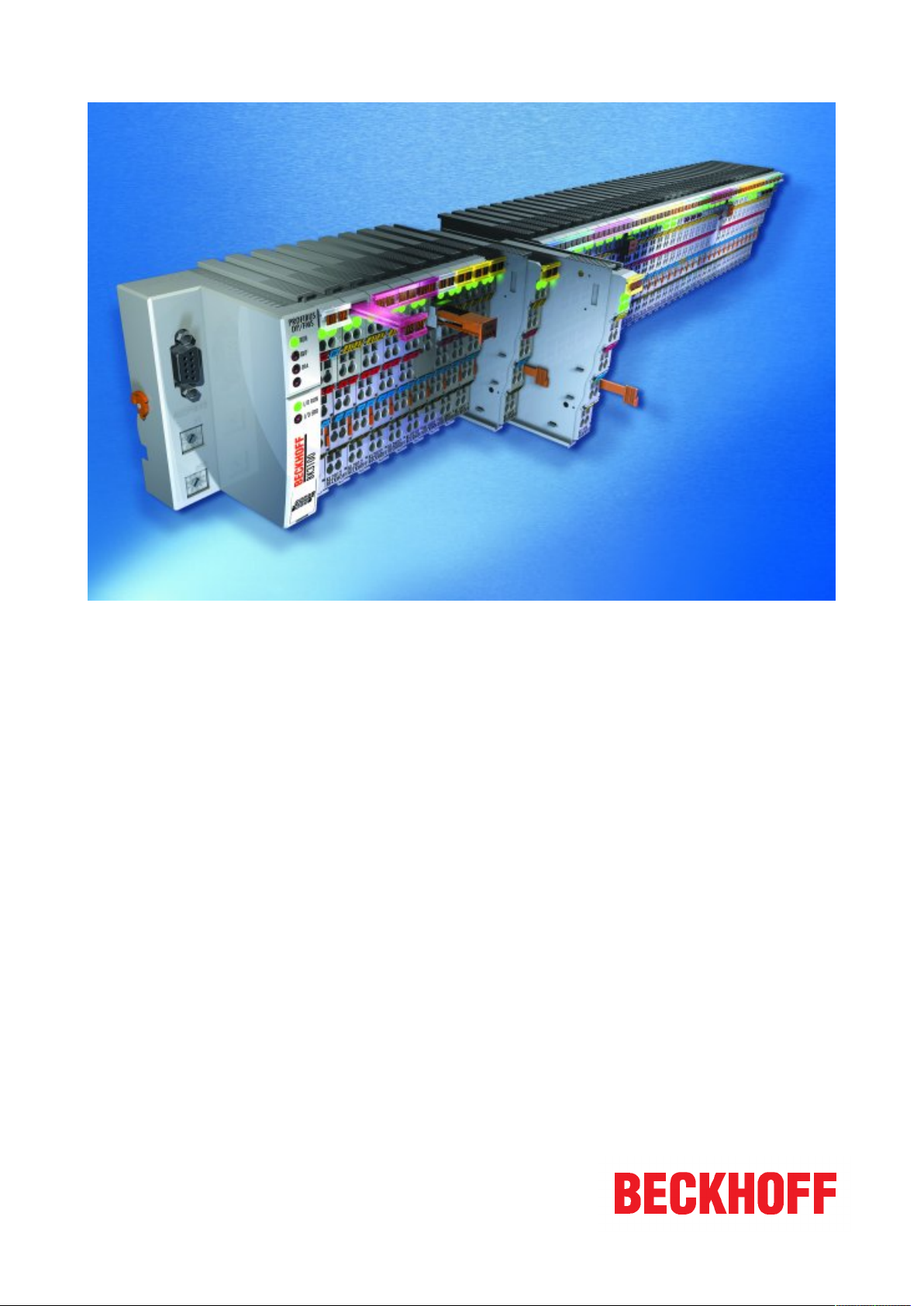
Page 1
Documentation
KL2535, KL2545
Pulse width current terminals
Version:
Date:
2.0.0
2016-02-29
Page 2

Page 3

Table of contents
Table of contents
1 Foreword ....................................................................................................................................................4
1.1 Notes on the documentation............................................................................................................. 4
1.2 Safety instructions ............................................................................................................................ 5
1.3 Documentation issue status.............................................................................................................. 6
2 Product overview.......................................................................................................................................7
2.1 KL2535 - Introduction ....................................................................................................................... 7
2.2 KL2535 - Technical Data .................................................................................................................. 8
2.3 KL2535 - LED displays ..................................................................................................................... 9
2.4 KL2545 - Introduction ..................................................................................................................... 10
2.5 KL2545 - Technical Data ................................................................................................................ 11
2.6 KL2545 - LED displays ................................................................................................................... 12
2.7 Pulse width modulation................................................................................................................... 13
2.8 Functions ........................................................................................................................................ 14
3 Mounting and wiring ...............................................................................................................................18
3.1 Installation on mounting rails .......................................................................................................... 18
3.2 Prescribed installation position ....................................................................................................... 20
3.3 Connection system ......................................................................................................................... 21
3.4 KL2535 - Connection ...................................................................................................................... 25
3.5 KL2545 - Connection ...................................................................................................................... 26
4 Configuration software KS2000 .............................................................................................................28
4.1 KS2000 - Introduction ..................................................................................................................... 28
4.2 Parameterization with KS2000 ....................................................................................................... 29
4.3 Settings........................................................................................................................................... 31
4.4 Register .......................................................................................................................................... 34
4.5 Process data................................................................................................................................... 35
5 Access from the user program ..............................................................................................................37
5.1 Process image ................................................................................................................................ 37
5.2 Control and status bytes ................................................................................................................. 38
5.3 Register overview ........................................................................................................................... 40
5.4 Register description ........................................................................................................................ 41
5.5 Examples of Register Communication............................................................................................ 45
5.5.1 Example 1: reading the firmware version from Register 9 of a terminal .............................45
5.5.2 Example 2: Writing to a user register..................................................................................45
6 Appendix ..................................................................................................................................................48
6.1 Support and Service ....................................................................................................................... 48
KL2535, KL2545 3Version: 2.0.0
Page 4

Foreword
1 Foreword
1.1 Notes on the documentation
This description is only intended for the use of trained specialists in control and automation engineering who
are familiar with the applicable national standards.
It is essential that the following notes and explanations are followed when installing and commissioning
these components.
The responsible staff must ensure that the application or use of the products described satisfy all the
requirements for safety, including all the relevant laws, regulations, guidelines and standards.
Disclaimer
The documentation has been prepared with care. The products described are, however, constantly under
development. For that reason the documentation is not in every case checked for consistency with
performance data, standards or other characteristics. In the event that it contains technical or editorial errors,
we retain the right to make alterations at any time and without warning. No claims for the modification of
products that have already been supplied may be made on the basis of the data, diagrams and descriptions
in this documentation.
Trademarks
Beckhoff®, TwinCAT®, EtherCAT®, Safety over EtherCAT®, TwinSAFE®, XFC® and XTS® are registered
trademarks of and licensed by Beckhoff Automation GmbH & Co. KG.
Other designations used in this publication may be trademarks whose use by third parties for their own
purposes could violate the rights of the owners.
Patent Pending
The EtherCAT Technology is covered, including but not limited to the following patent applications and
patents: EP1590927, EP1789857, DE102004044764, DE102007017835 with corresponding applications or
registrations in various other countries.
The TwinCAT Technology is covered, including but not limited to the following patent applications and
patents: EP0851348, US6167425 with corresponding applications or registrations in various other countries.
EtherCAT® is registered trademark and patented technology, licensed by Beckhoff Automation GmbH,
Germany
Copyright
© Beckhoff Automation GmbH & Co. KG, Germany.
The reproduction, distribution and utilization of this document as well as the communication of its contents to
others without express authorization are prohibited.
Offenders will be held liable for the payment of damages. All rights reserved in the event of the grant of a
patent, utility model or design.
KL2535, KL25454 Version: 2.0.0
Page 5
Foreword
1.2 Safety instructions
Safety regulations
Please note the following safety instructions and explanations!
Product-specific safety instructions can be found on following pages or in the areas mounting, wiring,
commissioning etc.
Exclusion of liability
All the components are supplied in particular hardware and software configurations appropriate for the
application. Modifications to hardware or software configurations other than those described in the
documentation are not permitted, and nullify the liability of Beckhoff Automation GmbH & Co. KG.
Personnel qualification
This description is only intended for trained specialists in control, automation and drive engineering who are
familiar with the applicable national standards.
Description of symbols
In this documentation the following symbols are used with an accompanying safety instruction or note. The
safety instructions must be read carefully and followed without fail!
Serious risk of injury!
Failure to follow the safety instructions associated with this symbol directly endangers the
DANGER
life and health of persons.
Risk of injury!
Failure to follow the safety instructions associated with this symbol endangers the life and
WARNING
health of persons.
Personal injuries!
Failure to follow the safety instructions associated with this symbol can lead to injuries to
CAUTION
persons.
Damage to the environment or devices
Failure to follow the instructions associated with this symbol can lead to damage to the en-
Attention
vironment or equipment.
Tip or pointer
This symbol indicates information that contributes to better understanding.
Note
KL2535, KL2545 5Version: 2.0.0
Page 6
Foreword
1.3 Documentation issue status
Version Comment
2.0.0 • Migration
1.5.0 • Technical data updated
1.4.0 • Product overview extended
1.3.0 • Mounting instructions updated
1.2.0 • Mounting instructions extended
• Technical data updated
• Register overview updated
1.1.0 • Connection description for the KL2535 corrected
• Basic function principles corrected
• Hardware version of the KL2535 corrected
1.0 First publication
0.1 Internal proof copy
Firmware and hardware versions
Documentation
version
1.5.0 1B 04 2B 08
1.4.0 1B 01 1B 05
1.3.0 1B 01 1B 05
1.2.0 1B 01 1B 05
1.1.0 1B 00 1A 02
1.0 1B 00 1A 02
0.1 1B 00 1A 02
The firmware and hardware versions (delivery state) can be taken from the serial number printed on the side
of the terminal.
KL2535 KL2545
Firmware Hardware Firmware Hardware
Syntax of the serial number
Structure of the serial number: WWYYFFHH
WW - week of production (calendar week)
YY - year of production
FF - firmware version
HH - hardware version
Example with ser. no.: 12 06 1A 02:
12 - week of production 12
06 - year of production 2006
1A - firmware version 1A
02 - hardware version 02
KL2535, KL25456 Version: 2.0.0
Page 7
2 Product overview
2.1 KL2535 - Introduction
Product overview
Fig.1: KL2535
The KL2535 two-channel pulse width current terminal regulates an output current by means of pulse width
control of the supply voltage. The current value (0A to 1A) is specified with 16-bit resolution by the
automation device.
The output stage is protected against overload and short-circuit and is electrically isolated from the K-bus.
Both channels indicate their state by LEDs, enabling fast on-the-spot diagnosis.
The Bus Terminal is available in the KL2535 version for standard wiring [}22] and the KS2535 for
permanent wiring [}21].
KL2535, KL2545 7Version: 2.0.0
Page 8

Product overview
2.2 KL2535 - Technical Data
Technical data KL2535/KS2535
Number of output stages 2
Load type ohmic/inductive > 1 mH
Supply for the output stage 24 VDC via power contacts
Output current per channel 1 A (short-circuit-proof, common thermal overload
warning for both output stages)
PWM clock frequency 36 kHz
Resolution max. 12 bit
Number of digital inputs 2 digital inputs (24 V)
Nominal voltage of the inputs 24VDC (-15%/+20%)
Signal voltage “0” -3 V... 2 V
Signal voltage “1” 15 V... 30 V
Input filter 0.2ms
Input current typically 5 mA
Electrical isolation 500 V (K-bus/mains voltage)
Supply voltage for internal E-bus circuit via the K-bus
Current consumption from K-bus typically: 60 mA
Current consumption from the power contacts typically: 10 mA
Bit width in the input process image 2 x 16 bit data, 2 x 8 bit status
Bit width in the output process image 2 x 16 bit data, 2 x 8 bit control
Configuration via the Bus Coupler or the controller
Weight approx. 55 g
Permissible ambient temperature range during
operation
Permissible ambient temperature range during
storage
Permissible relative humidity 95%, no condensation
Dimensions (W x H x D) approx. 15 mm x 100 mm x 70 mm (width aligned: 12
Mounting [}18]
Vibration/shock resistance conforms to EN 60068-2-6 / EN 60068-2-27
EMC immunity/emission conforms to EN 61000-6-2 / EN 61000-6-4
Protection class IP20
Correct installation position
Approval CE
0°C ... + 55°C
-25°C ... + 85°C
mm)
on 35 mm mounting rail conforms to EN 60715
see section Installation position [}20]
KL2535, KL25458 Version: 2.0.0
Page 9

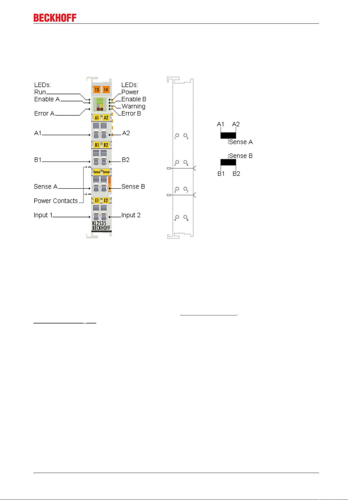
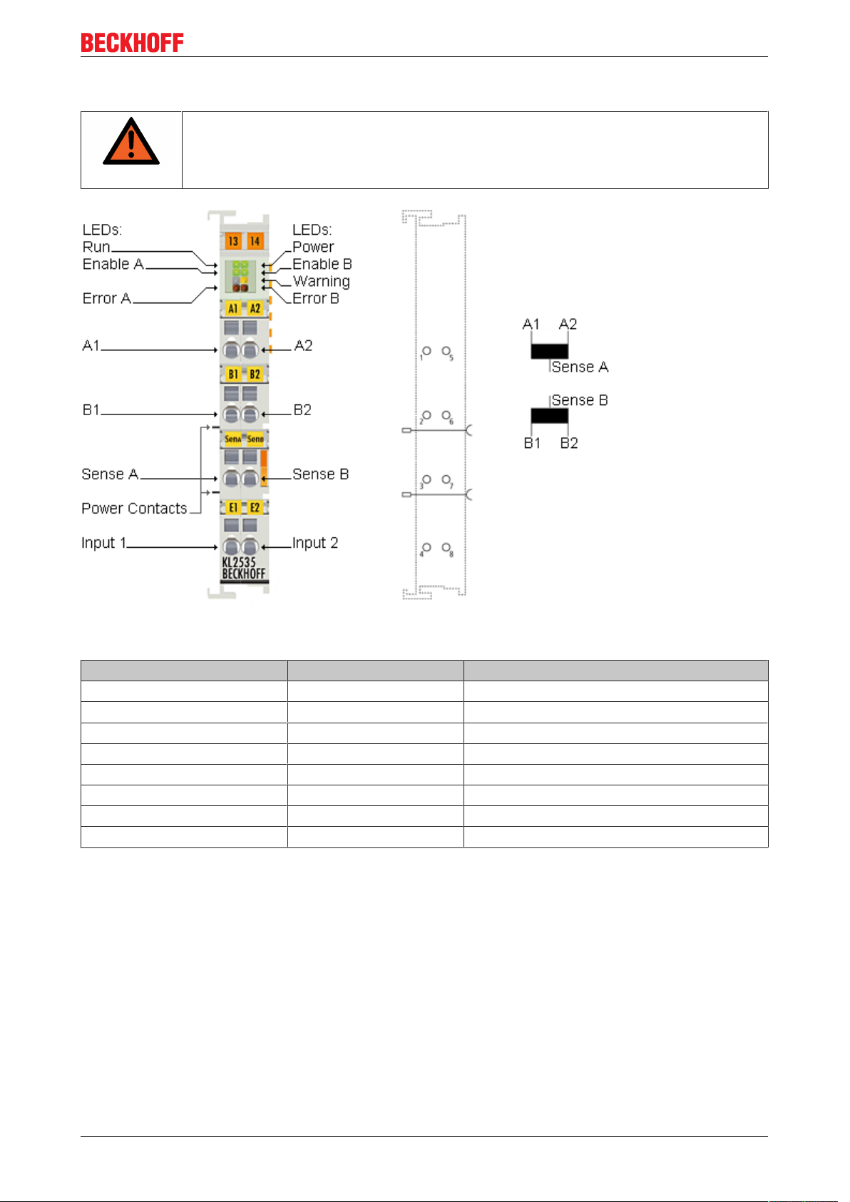
2.3 KL2535 - LED displays
LED indicators
Product overview
Fig.2: KL2535 - LEDs
LED Display
Run (green) reserved Data transmission on the K-bus is active
Enable A (green) off Channel 1 is either not enabled or not ready to operate.
on Channel 1 is enabled and is ready to operate.
- reserved
Error A (red) on There is an error at channel 1
Power (green) off The power supply voltage is absent (less than 7 V).
on The power supply voltage is present (more than 8 V).
Enable B (green) off Channel 2 is either not enabled or not ready to operate.
on Channel 2 is enabled and is ready to operate.
Warning (yellow) on The internal temperature has risen to more than 80°C, or the power supply
voltage has dropped.
Error B (red) on There is an error at channel 2
KL2535, KL2545 9Version: 2.0.0
Page 10

Product overview
2.4 KL2545 - Introduction
Fig.3: KL2545
The KL2545 two-channel pulse width current terminal regulates an output current by means of pulse width
control of the supply voltage. The current value (0A to 3.5 A) is specified with 16-bit resolution by the
automation device.
The output stage is protected against overload and short-circuit and is electrically isolated from the K-bus.
Both channels indicate their state by LEDs, enabling fast on-the-spot diagnosis. An incremental encoder can
be connected to each channel for the implementation of the position feedback directly in the terminal.
The Bus Terminal is available in the KL2545 version for standard wiring [}22] and the KS2545 for
permanent wiring [}21].
KL2535, KL254510 Version: 2.0.0
Page 11

Product overview
2.5 KL2545 - Technical Data
Technical data KL2545/KS2545
Number of output stages 2
Load type ohmic/inductive > 1 mH
Supply for the output stage 8 VDC to 50 VDC, via terminal locations
Output current per channel 3.5 A (short-circuit-proof, common thermal overload
warning for both output stages)
PWM clock frequency 36 kHz
Resolution max. 12 bit
Number of digital inputs 2 (for end positions)
Rated voltage of the digital inputs 24VDC (-15%/+20%)
Signal voltage “0” at digital inputs -3V... 2V
Signal voltage “1” at digital inputs 15V... 30V
Input filter 0.2ms
Input current typically 5 mA
Number of encoder inputs 4 (for an encoder system)
Encoder voltage "0" -3V ... 1.5V
Encoder voltage "1" 2.5 V ... 24 V
Electrical isolation 500 V (K-bus/mains voltage)
Supply voltage for internal E-bus circuit via the K-bus
Current consumption from K-bus typically: 100 mA
Current consumption from the power contacts typically: 20 mA
Power loss typically: 4 W
Bit width in the input process image 2 x 16 bit data, 2 x 8 bit status
Bit width in the output process image 2 x 16 bit data, 2 x 8 bit control
Configuration via the Bus Coupler or the controller
Weight approx. 100 g
Permissible ambient temperature range during
operation
Permissible ambient temperature range during
storage
Permissible relative humidity 95%, no condensation
Dimensions (W x H x D) approx. 27 mm x 100 mm x 70 mm (width aligned: 24
Mounting [}18]
Vibration/shock resistance conforms to EN 60068-2-6 / EN 60068-2-27
EMC immunity/emission conforms to EN 61000-6-2 / EN 61000-6-4
Protection class IP20
Correct installation position
Approval CE
0°C ... + 55°C
-25°C ... + 85°C
mm)
on 35 mm mounting rail conforms to EN 60715
see section Installation position [}20]
KL2535, KL2545 11Version: 2.0.0
Page 12

Product overview
2.6 KL2545 - LED displays
Fig.4: KL2545 - LEDs
Left LED prism
LED Display
Run (green) on Data transmission on the K-bus is active
Enc. A: A (green) on There is a signal at input A for encoder A.
Enc. B: A (green) on There is a signal at input A for encoder B.
Input1 (green) on There is a signal at input 1.
- reserved
Enc. A: B (green) on There is a signal at input B for encoder A.
Enc. B: B (green) on There is a signal at input B for encoder B.
Input2 (green) on There is a signal at input 2.
Right LED prism
LED Display
- reserved
Enable A (green) off Channel 1 is either not enabled or not ready to operate.
on Channel 1 is enabled and is ready to operate.
- reserved
Error A (red) on There is an error at channel 1
Load Power (green) off The power supply voltage for the load is absent (less than 7 V).
on The power supply voltage for the load is present (more than 8 V).
Enable B (green) off Channel 2 is either not enabled or not ready to operate.
on Channel 2 is enabled and is ready to operate.
Warning (yellow) on The internal temperature has risen to more than 80°C, or the power supply voltage has
Error B (red) on There is an error at channel 2
dropped.
KL2535, KL254512 Version: 2.0.0
Page 13
Product overview
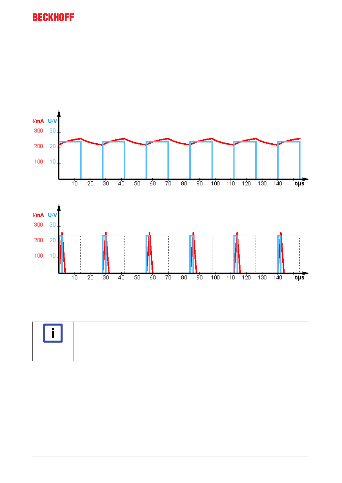
2.7 Pulse width modulation
The KL2535 and KL2545 pulse-width current terminals include an integrated PWM output stage (up to 175
W) in a very compact design.
By means of the PWM output stage the pulse width modulation (PWM) of the supply voltage is used to
regulate the output current of a connected ohmic/inductive load. The full supply voltage, pulsating with a
certain frequency, is thereby fed to the output. A load current only develops at the inductance at the high
level. The load current is not changed by changing the voltage level, but by the duration of the switch-off
(pulse width) in relation to the period duration. This results in a duty factor corresponding to the pulse width
divided by the period duration of between 0 and 100% and is proportional to the load current.
Fig.5: Operation at load with adequate inductance
Fig.6: Operation at load inadequate inductance (near ohmic)
The figure "Operation at load with inadequate inductance" illustrates operation with an inadequate
inductance. Continuous current flow is not reached. The current has "gaps". This mode of operation is not
permitted.
Pulse width current terminals require inductive loads
The load inductance should have a minimum inductance of 1 mH. Operation of the pulse
Note
width current terminals at loads with an inductance of less than 1 mH is not recommended,
since the intermittent current flow prevents reference between the set value and the arithmetic mean of the current.
KL2535, KL2545 13Version: 2.0.0
Page 14

Product overview
2.8 Functions
The KL2535 and KL2545 pulse-width current terminals include an integrated PWM output stage (up to 175
W) in a very compact design.
General functions
Enable/Readiness for operation
The enable bit CB1.5 [}38] in the control byte must be set in order to activate the output stage. If the
terminal is not subject to an error at this time, it acknowledges the command by setting the ready bit, SB1.4
[}38], in the status byte
Setting/deleting the position (KL2545 only)
The current position value of the encoder can be set or deleted by the user. Register R1 [}41] is the
reference for this. A rising edge at bit CB1.1 [}38] sets the current position, and the acknowledgement is
provided through status bit SB1.1 [}38].
Latch functions
The internal encoder offers the option of registering a latch event. A latch event can be generated via the
digital input signals.
The terminal response to the latch events is activated as follows:
• Setting the control bit CB1.2 [}38] activates the rising edge at the digital input (highest priority)
• Setting the control bit CB1.3 [}38] activates the falling edge at the digital input (second-highest
priority)
Once the user has enabled the function, during the next latch event, the terminal saves the current position
value and indicates this by setting status bit SB1.2 [}38]. Reading out the latch value must be started by
setting CB1.4 [}38]; this will map the latch value into the DataIN process data (the terminal indicates this
through status bit SB1.3 [}38]).
Enable for latch values
The enable that was set previously must be retained while reading out the latch value. The
Note
latch values are lost if the enable is removed!
Digital inputs
The digital inputs are mapped into the status byte in bit SB1.0 [}38].
Error indication
The terminal offers the user a variety of diagnostic options. These messages are divided into hardware
warnings and hardware errors.
Hardware warnings
When one of the following warning occurs, bit SB1.5 [}38] (Warning) is set in the status byte.
• OverTemperature R0.8 [}41]
(If the temperature inside the terminal reaches 80°C, bit SB1.5 [}38] (Warning) is set. The bit is
automatically reset if the temperature falls below 60°C.
• LowVoltage R0.9 [}41]
KL2535, KL254514 Version: 2.0.0
Page 15
Product overview
Hardware error
If one of the following errors occurs, the load is de-energized and bit SB1.6 [}38] (Error) is set in the Status
byte.
• UnderVoltage R0.11 [}41]
• OverCurrent, R0.12 [}41]
• Open load / broken wire (OpenLoad, R0.13 [}41])
• Failure of the 24 V control supply (NoControlPower, R0.14 [}41])
(The terminal is automatically reinitialized when the control voltage returns)
If an error occurs, it first has to be rectified and subsequently acknowledged and thus cancelled by setting bit
CB1.6 [}38] in the control byte.
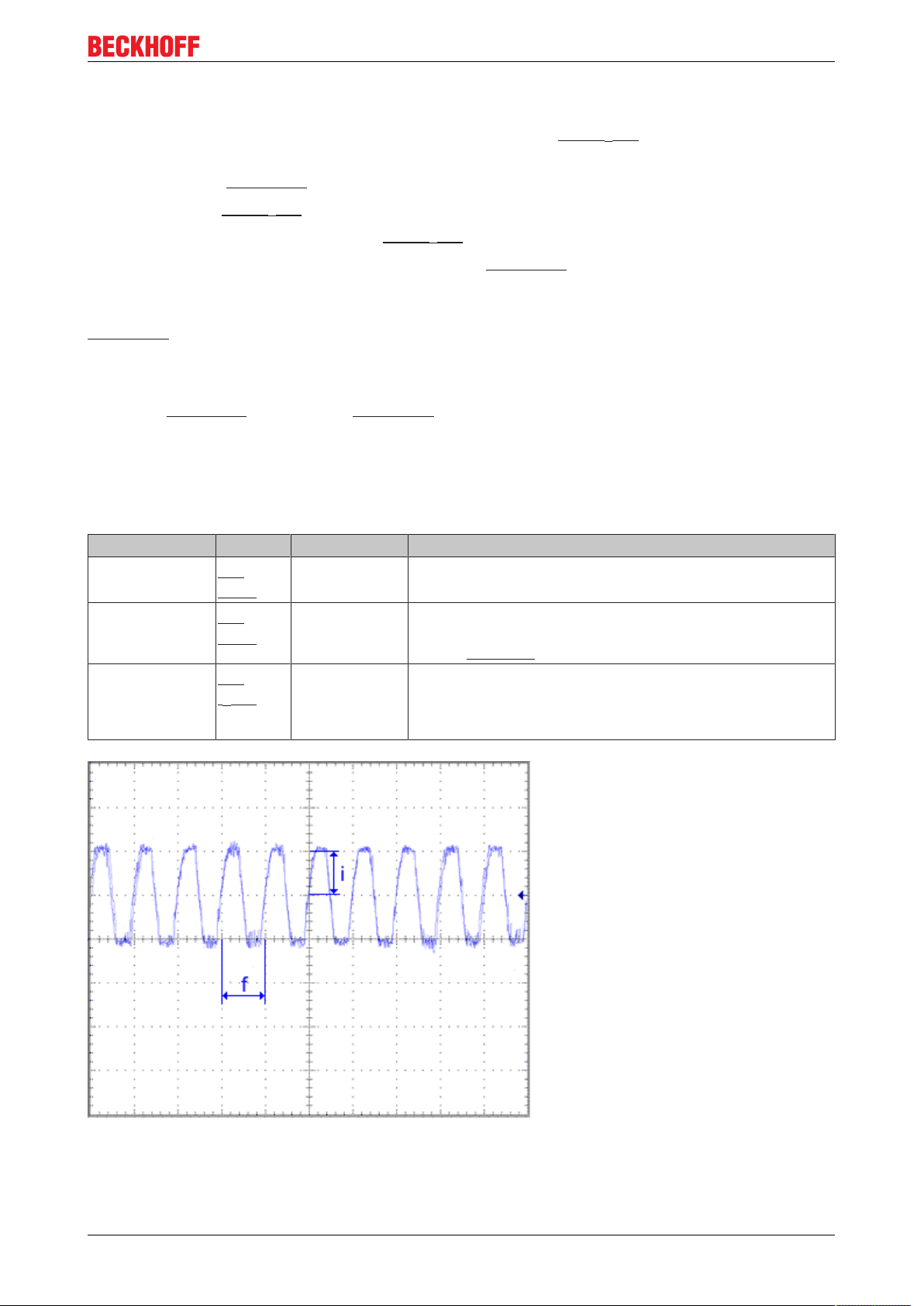
Dithering
Feature bit R32.5 [}43] and control bit CB1.0 [}38] must be set to activate the dither.
The purpose of this function is to eliminate magnetization effects. Dithering involves modulating a
rectangular signal on top of the actual output value. The configuration required for this depends a lot on the
particular application. It must be determined with the aid of the characteristic data of whatever actuator is
connected.
The following parameters can be set:
Name Register Value range Description
Frequency - f
Amplitude - i
Switch-off ramp t
R37
[}44]
R38
[}44]
R39
[}44]
10 Hz to 500 Hz The frequency of the rectangular signal; the resolution of the
setting is 1 Hz.
0% to 100% The amplitude of the rectangular signal; the resolution is 1%
(with reference to the output current that has been set in
register R36 [}43])
0ms to
32767ms
When switched on, the dither signal jumps immediately to the
amplitude set in R38. When switched off, the signal is
attenuated linearly over the time configured here; the
resolution is 1 ms.
Fig.7: Frequency - f / Amplitude - i
KL2535, KL2545 15Version: 2.0.0
Page 16

Product overview
Fig.8: Switch-off ramp - t
Valve curve
Feature bit R32.4 [}43] must be set in order to activate the valve curve.
The following parameters can be set:
Name Regis-
ter
Overlap threshold value - x
1
R40
[}44]
Overlap output value - y
1
R41
[}44]
Bend compensation -threshold
value- x
2
Bend compensation - output value y
2
Area compensation - threshold
value - x
3
R42
[}44]
R43
[}44]
R44
[}44]
Value range Description
0 to 1000 The overlap range ends at this process data
value; the resolution is 0.1% (as a fraction of
32767)
0 to 1000 The maximum output current in the overlap
region; the resolution is 0.1% (with reference
to the output current that has been set in
register R36 [}43])
0 to 1000 The bend compensation range ends at this
process data value; the resolution is 0.1% (as
a fraction of 32767)
0 to 1000 The maximum output current in the bend
compensation region; the resolution is 0.1%
(with reference to the output current that has
been set in register R36 [}43])
0 to 1000 The area compensation region ends at this
process data value; the resolution is 0.1% (as
a fraction of 32767)
The characteristic curve is divided into four regions:
I Overlapping
II Bend compensation
III, III' Area compensation
IV End region
KL2535, KL254516 Version: 2.0.0
Page 17

Product overview
Fig.9: Valve curve
Process data ramps
Feature bit R32.6 [}43] must be set in order to activate the process data ramps.
This function offers the facility for automatically changing the output current from the current process data
value to the new one up or down along a linear ramp. The values of registers R45 and R46 here are related
to the entire process data range, i.e. from 0 to 32767.
The following parameters can be set:
Name Register Value range Description
Rising ramp - t
Falling ramp - t
R45
1
[}44]
R46
2
[}45]
0 to 32767 ms The time, t1, required for the process data value to rise from 0
to 32767 (resolution: 1 ms).
0 to 32767 ms The time, t2, required for the process data value to fall from
32767 to 0 (resolution: 1ms).
Fig.10: Process data ramps
KL2535, KL2545 17Version: 2.0.0
Page 18

Mounting and wiring
3 Mounting and wiring
3.1 Installation on mounting rails
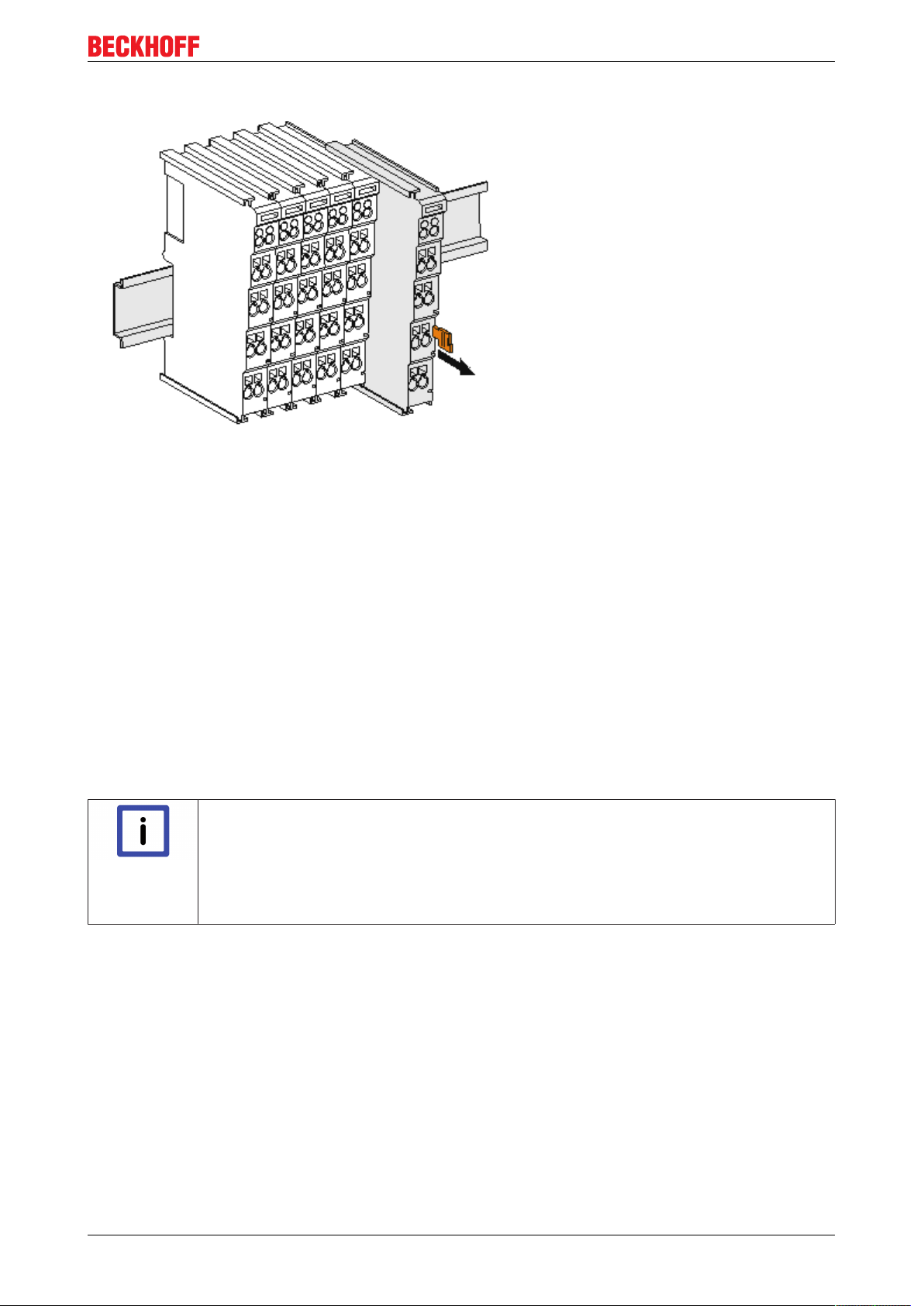
Risk of electric shock and damage of device!
Bring the bus terminal system into a safe, powered down state before starting installation,
WARNING
Assembly
disassembly or wiring of the Bus Terminals!
Fig.11: Attaching on mounting rail
The Bus Coupler and Bus Terminals are attached to commercially available 35mm mounting rails (DIN rails
according to EN60715) by applying slight pressure:
1. First attach the Fieldbus Coupler to the mounting rail.
2. The Bus Terminals are now attached on the right-hand side of the Fieldbus Coupler. Join the
components with tongue and groove and push the terminals against the mounting rail, until the lock
clicks onto the mounting rail.
If the Terminals are clipped onto the mounting rail first and then pushed together without tongue and
groove, the connection will not be operational! When correctly assembled, no significant gap should
be visible between the housings.
Fixing of mounting rails
The locking mechanism of the terminals and couplers extends to the profile of the mounting
Note
rail. At the installation, the locking mechanism of the components must not come into conflict with the fixing bolts of the mounting rail. To mount the mounting rails with a height of
7.5mm under the terminals and couplers, you should use flat mounting connections (e.g.
countersunk screws or blind rivets).
KL2535, KL254518 Version: 2.0.0
Page 19
Mounting and wiring
Disassembly
Fig.12: Disassembling of terminal
Each terminal is secured by a lock on the mounting rail, which must be released for disassembly:
1. Pull the terminal by its orange-colored lugs approximately 1cm away from the mounting rail. In doing
so for this terminal the mounting rail lock is released automatically and you can pull the terminal out of
the bus terminal block easily without excessive force.
2. Grasp the released terminal with thumb and index finger simultaneous at the upper and lower grooved
housing surfaces and pull the terminal out of the bus terminal block.
Connections within a bus terminal block
The electric connections between the Bus Coupler and the Bus Terminals are automatically realized by
joining the components:
• The six spring contacts of the K-Bus/E-Bus deal with the transfer of the data and the supply of the Bus
Terminal electronics.
• The power contacts deal with the supply for the field electronics and thus represent a supply rail within
the bus terminal block. The power contacts are supplied via terminals on the Bus Coupler (up to 24V)
or for higher voltages via power feed terminals.
Power Contacts
During the design of a bus terminal block, the pin assignment of the individual Bus Termi-
Note
nals must be taken account of, since some types (e.g. analog Bus Terminals or digital 4channel Bus Terminals) do not or not fully loop through the power contacts. Power Feed
Terminals (KL91xx, KL92xx or EL91xx, EL92xx) interrupt the power contacts and thus represent the start of a new supply rail.
PE power contact
The power contact labeled PE can be used as a protective earth. For safety reasons this contact mates first
when plugging together, and can ground short-circuit currents of up to 125A.
KL2535, KL2545 19Version: 2.0.0
Page 20

Mounting and wiring
Fig.13: Power contact on left side
Possible damage of the device
Note that, for reasons of electromagnetic compatibility, the PE contacts are capacitatively
Attention
coupled to the mounting rail. This may lead to incorrect results during insulation testing or
to damage on the terminal (e.g. disruptive discharge to the PE line during insulation testing
of a consumer with a nominal voltage of 230V). For insulation testing, disconnect the PE
supply line at the Bus Coupler or the Power Feed Terminal! In order to decouple further
feed points for testing, these Power Feed Terminals can be released and pulled at least
10mm from the group of terminals.
Risk of electric shock!
The PE power contact must not be used for other potentials!
WARNING
3.2 Prescribed installation position
Constraints regarding installation position and operating temperature range
When installing the terminals ensure that an adequate spacing is maintained between other
Attention
Prescribed installation position
components above and below the terminal in order to guarantee adequate ventilation!
The prescribed installation position requires the mounting rail to be installed horizontally and the connection
surfaces of the EL/KL terminals to face forward (see Fig. Recommended distances for standard installation
position).
The terminals are ventilated from below, which enables optimum cooling of the electronics through
convection. "From below" is relative to the acceleration of gravity.
KL2535, KL254520 Version: 2.0.0
Page 21

Mounting and wiring
Fig.14: Recommended distances for standard installation position
Compliance with the distances shown in Fig. Recommended distances for standard installation position is
strongly recommended.
3.3 Connection system
Risk of electric shock and damage of device!
Bring the bus terminal system into a safe, powered down state before starting installation,
WARNING
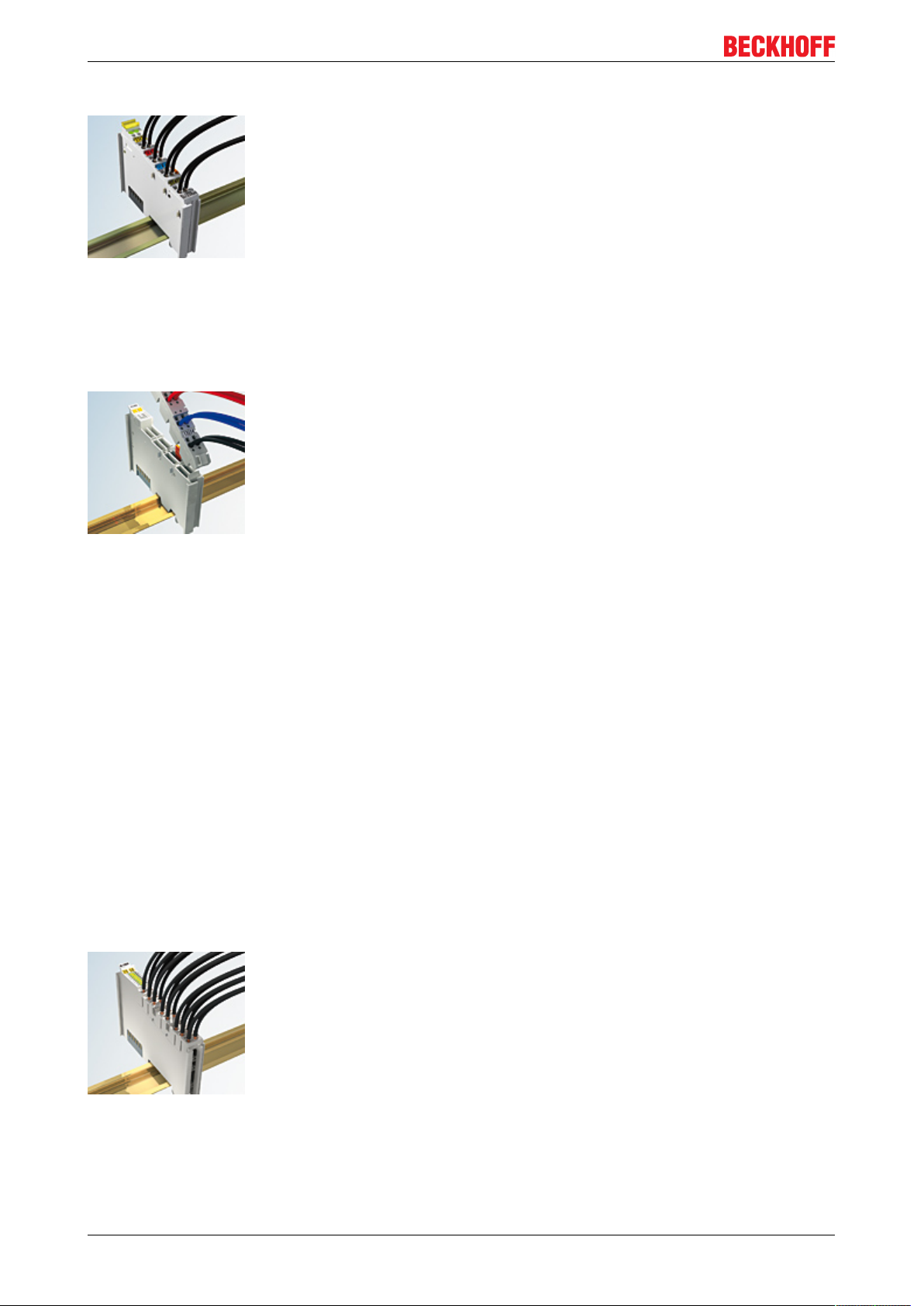
Overview
The Bus Terminal system offers different connection options for optimum adaptation to the respective
application:
• The terminals of KLxxxx and ELxxxx series with standard wiring include electronics and connection
level in a single enclosure.
• The terminals of KSxxxx and ESxxxx series feature a pluggable connection level and enable steady
wiring while replacing.
• The High Density Terminals (HD Terminals) include electronics and connection level in a single
enclosure and have advanced packaging density.
disassembly or wiring of the Bus Terminals!
KL2535, KL2545 21Version: 2.0.0
Page 22
Mounting and wiring
Standard wiring
Fig.15: Standard wiring
The terminals of KLxxxx and ELxxxx series have been tried and tested for years.
They feature integrated screwless spring force technology for fast and simple assembly.
Pluggable wiring
Fig.16: Pluggable wiring
The terminals of KSxxxx and ESxxxx series feature a pluggable connection level.
The assembly and wiring procedure for the KS series is the same as for the KLxxxx and ELxxxx series.
The KS/ES series terminals enable the complete wiring to be removed as a plug connector from the top of
the housing for servicing.
The lower section can be removed from the terminal block by pulling the unlocking tab.
Insert the new component and plug in the connector with the wiring. This reduces the installation time and
eliminates the risk of wires being mixed up.
The familiar dimensions of the terminal only had to be changed slightly. The new connector adds about 3
mm. The maximum height of the terminal remains unchanged.
A tab for strain relief of the cable simplifies assembly in many applications and prevents tangling of individual
connection wires when the connector is removed.
Conductor cross sections between 0.08mm2 and 2.5mm2 can continue to be used with the proven spring
force technology.
The overview and nomenclature of the product names for KSxxxx and ESxxxx series has been retained as
known from KLxxxx and ELxxxx series.
High Density Terminals (HD Terminals)
Fig.17: High Density Terminals
The Bus Terminals from these series with 16 connection points are distinguished by a particularly compact
design, as the packaging density is twice as large as that of the standard 12mm Bus Terminals. Massive
conductors and conductors with a wire end sleeve can be inserted directly into the spring loaded terminal
point without tools.
KL2535, KL254522 Version: 2.0.0
Page 23
Mounting and wiring
Wiring HD Terminals
The High Density (HD) Terminals of the KLx8xx and ELx8xx series doesn't support steady
Note
wiring.
Ultrasonically "bonded" (ultrasonically welded) conductors
Ultrasonically “bonded" conductors
It is also possible to connect the Standard and High Density Terminals with ultrasonically
Note
"bonded" (ultrasonically welded) conductors. In this case, please note the tables concerning the wire-size width [}23] below!
Wiring
Terminals for standard wiring ELxxxx / KLxxxx and terminals for steady wiring
ESxxxx / KSxxxx
Fig.18: Mounting a cable on a terminal connection
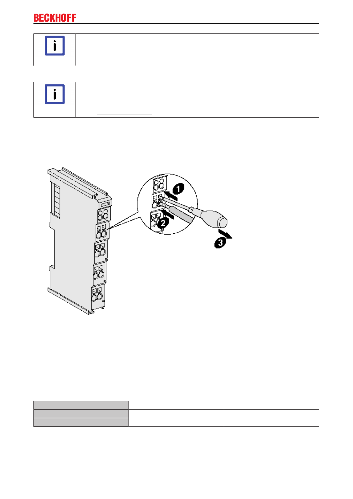
Up to eight connections enable the connection of solid or finely stranded cables to the Bus Terminals. The
terminals are implemented in spring force technology. Connect the cables as follows:
1. Open a spring-loaded terminal by slightly pushing with a screwdriver or a rod into the square opening
above the terminal.
2. The wire can now be inserted into the round terminal opening without any force.
3. The terminal closes automatically when the pressure is released, holding the wire securely and
permanently.
Terminal housing ELxxxx, KLxxxx ESxxxx, KSxxxx
Wire size width 0.08 ... 2,5mm
Wire stripping length 8 ... 9mm 9 ... 10mm
KL2535, KL2545 23Version: 2.0.0
2
0.08 ... 2.5mm
2
Page 24
Mounting and wiring
High Density Terminals ELx8xx, KLx8xx (HD)
The conductors of the HD Terminals are connected without tools for single-wire conductors using the direct
plug-in technique, i.e. after stripping the wire is simply plugged into the contact point. The cables are
released, as usual, using the contact release with the aid of a screwdriver. See the following table for the
suitable wire size width.
Terminal housing High Density Housing
Wire size width (conductors with a wire end sleeve) 0.14... 0.75mm
Wire size width (single core wires) 0.08 ... 1.5mm
Wire size width (fine-wire conductors) 0.25 ... 1.5mm
Wire size width (ultrasonically “bonded" conductors)
only 1.5mm2 (see notice
2
2
2
[}23]!)
Wire stripping length 8 ... 9mm
Shielding
Shielding
Analog sensors and actors should always be connected with shielded, twisted paired wires.
Note
KL2535, KL254524 Version: 2.0.0
Page 25
3.4 KL2535 - Connection
Risk of injury through electric shock and damage to the device!
Bring the Bus Terminals system into a safe, de-energized state before starting mounting,
disassembly or wiring of the Bus Terminals.
WARNING
Mounting and wiring
Fig.19: KL2535 Connection
Terminal point No. Connection
A1 1 Load A, connection A1
B1 2 Load B, connection B1
Sense A 3 Load A, sense
Input 1 4 Digital input 1 (24 VDC).
A2 5 Load A, connection A2
B2 6 Load B, connection B2
Sense B 7 Load B, sense
Input 2 8 Digital input 2 (24 VDC).
KL2535, KL2545 25Version: 2.0.0
Page 26

Mounting and wiring
3.5 KL2545 - Connection
Risk of injury through electric shock and damage to the device!
Bring the Bus Terminals system into a safe, de-energized state before starting mounting,
WARNING
disassembly or wiring of the Bus Terminals.
Fig.20: KL2545 Connection
Left-hand section of the housing
Terminal point No. Connection for
EncoderA, A 1 EncoderA, connectionA
Encoder B, A 2 Encoder B, connectionA
Encoder Power +24V 3 Encoder supply (from positive power contact)
Input 1 4 Digital input 1 (24 VDC).
The current counter value is saved as a reference mark in the latch register if
bit CW.1 is set in the control word and a rising edge occurs at digital input 1.
Encoder A, B 5 EncoderA, connectionB
Encoder B, B 6 EncoderB, connectionB
Encoder Power 0 V 7 Encoder supply (from negative power contact)
Input 2 8 Digital input 2 (24 VDC).
The current counter value is saved as a reference mark in the latch register if
bit CW.2 is set in the control word and a rising edge occurs at digital input 2.
KL2535, KL254526 Version: 2.0.0
Page 27

Right-hand section of the housing
Mounting and wiring
Terminal point
(right)
Load A, A1 1' Load A, connection A1
Load B, B1 2' Load B, connection B1
Sense A 3' Load A, sense
Load Power 50V 4' Power supply for supplying the load (maximum +50VDC)
Load A, A2 5' Load A, connection A2
Load B, B2 6' Load B, connection B2
Sense B 7' Load B, sense
Load Power 0 V 8' Power supply for supplying the load (0VDC)
No. Connection for
Power contacts
The voltage Up of the power contacts (+24VDC) supplies the following consumers:
• Incremental encoder (terminal points 3 and 7)
• Digital inputs (terminal points 4 and 8)
• Output stage driver of the pulse width current terminal
Order of switch-on of the supply voltages
The voltage Up must already be present at the power contacts when the K-bus voltage is
Note
switched on so that the internal circuits (output stage drivers) can be initialized.
If this is not possible due to the application (supply is switched, for example, via emergency
stop circuit), the terminal performs a software reset after the system starts up.
If the voltage Up at the power contacts fails, this is indicated by bit SW.14. The return of the
voltage is automatically detected and an initialization is performed.
WARNING
Valves are not reset if the K-bus voltage fails!
If the K-bus voltage fails (5 V, supplied from the supply voltage Us of the Bus Coupler), the
output drivers are not reset! This means that the valves are then not driven back to the initial position!
KL2535, KL2545 27Version: 2.0.0
Page 28

Configuration software KS2000
4 Configuration software KS2000
4.1 KS2000 - Introduction
The KS2000 configuration software permits configuration, commissioning and parameterization of bus
couplers, of the affiliated bus terminals and of Fieldbus Box Modules. The connection between bus coupler/
Fieldbus Box Module and the PC is established by means of the serial configuration cable or the fieldbus.
Fig.21: KS2000 configuration software
Configuration
You can configure the Fieldbus stations with the Configuration Software KS2000 offline. That means, setting
up a terminal station with all settings on the couplers and terminals resp. the Fieldbus Box Modules can be
prepared before the commissioning phase. Later on, this configuration can be transferred to the terminal
station in the commissioning phase by means of a download. For documentation purposes, you are provided
with the breakdown of the terminal station, a parts list of modules used and a list of the parameters you have
modified. After an upload, existing fieldbus stations are at your disposal for further editing.
Parameterization
KS2000 offers simple access to the parameters of a fieldbus station: specific high-level dialogs are available
for all bus couplers, all intelligent bus terminals and Fieldbus Box modules with the aid of which settings can
be modified easily. Alternatively, you have full access to all internal registers of the bus couplers and
intelligent terminals. Refer to the register description for the meanings of the registers.
KL2535, KL254528 Version: 2.0.0
Page 29

Configuration software KS2000
Commissioning
The KS2000 software facilitates commissioning of machine components or their fieldbus stations: Configured
settings can be transferred to the fieldbus modules by means of a download. After a login to the terminal
station, it is possible to define settings in couplers, terminals and Fieldbus Box modules directly online. The
same high-level dialogs and register access are available for this purpose as in the configuration phase.
The KS2000 offers access to the process images of the bus couplers and Fieldbus Box modules.
• Thus, the coupler's input and output images can be observed by monitoring.
• Process values can be specified in the output image for commissioning of the output modules.
All possibilities in the online mode can be used in parallel with the actual fieldbus mode of the terminal
station. The fieldbus protocol always has the higher priority in this case.
4.2 Parameterization with KS2000
Connect the configuration interface of your fieldbus coupler with the serial interface of your PC via the
configuration cable and start the KS2000 configuration software.
Click on the Login button. The configuration software will now load the information for
the connected fieldbus station.
In the example shown, this is
• Bus Coupler for Ethernet BK9000.
• a KL1xx2 digital input terminal.
• a KL2535 or KL2545 two-channel pulse width current terminal.
• a KL9010 bus end terminal.
KL2535, KL2545 29Version: 2.0.0
Page 30

Configuration software KS2000
Fig.22: Display of the fieldbus station in KS2000
The left-hand KS2000 window displays the terminals of the fieldbus station in a tree structure.
The right-hand KS2000 window contains a graphic display of the fieldbus station terminals.
In the tree structure of the left-hand window, click on the plus-sign next to the terminal whose parameters
you wish to change (item 2 in the example).
Fig.23: KS2000 tree branches for channel 1 of the KL2535
For the KL2535, the branches Register, Settings and ProcData are displayed:
• Register [}34] permits direct access to the registers of the KL2535.
• Under Settings [}31] you find dialog boxes for parameterizing the KL2535.
KL2535, KL254530 Version: 2.0.0
Page 31

• ProcData [}35] displays the KL2535 process data.
4.3 Settings
Settings for parameterization of the KL2535 and KL2545.
Configuration software KS2000
Fig.24: Settings via KS2000
Operation mode
Watchdog timer active (R32.2 [}43])
Here you can deactivate the watchdog (default: active). If the pulse-width current terminal fails to receive any
process data from the controller for 100 ms while the watchdog is active, the watchdog triggers and the valve
is switched off.
User scaling (R32.0 [}43])
You can activate user scaling here (the default is deactivated).
User switch-on value active (R32.8 [}43])
You can activate the user switch-on value [}32]here (the default is inactive).
Sign / amount representation (R32.3 [}43])
You can activate the sign / amount representation here (the default is inactive).
KL2535, KL2545 31Version: 2.0.0
Page 32

Configuration software KS2000
Dithering active (R32.5 [}43])
You can activate the dithering [}15]here (the default is inactive).
Valve curve (R32.4 [}43])
You can activate the valve curve [}16]here (the default is inactive).
Process data ramps active (R32.6 [}43])
You can activate the process data ramps [}17] here (the default is inactive).
Register values
User offset (R33 [}43])
You can specify the offset for the user-scaling here (the default is 0).
User gain (R34 [}43])
The gain for the user scaling can be set here (default: 4096
dec
).
User switch-on value (R35 [}43])
You can specify the offset for the user switch-on value for the speed here (the default is 0).
Max. output current (R36 [}43])
You can specify the maximum output current here.
KL2535: The default is 1000 mA
KL2545: The default is 3,500 mA
Dithering frequency (R37 [}44])
You can specify the frequency of the dither [}15]here (the default is 0).
Dithering amplitude (R38 [}44])
You can specify the amplitude of the dither [}15]here (the default is 0).
Dithering switch-off ramp (R39 [}44])
You can specify the switch-off ramp of the dither [}15]here (the default is 0).
Overlap threshold value (R40 [}44])
You can specify the threshold value of the overlap region [}16]here (the default is 0).
Overlap output value (R41 [}43])
You can specify the output value of the overlap region [}16]here (the default is 0).
Bend threshold value (R42 [}44])
You can specify the threshold value of the bend compensation region [}16] here (the default is 0).
KL2535, KL254532 Version: 2.0.0
Page 33

Configuration software KS2000
Bend region output value (R43 [}44])
You can specify the output value of the bend compensation region [}16] here (the default is 0).
The I-component of the velocity control is attenuated towards the zero point. This register specifies the value
from which the attenuation is activated.
Area compensation - threshold value (R44 [}44])
You can specify the threshold value of the area compensation region [}16]here (the default is 1000
Process data ramp (rising) (R45 [}44])
You can specify the rising process data ramp [}17]here (the default is 0
dec
).
Process data ramp (falling) (R38 [}43])
You can specify the falling process data ramp [}17]here (the default is 0
dec
).
dec
).
KL2535, KL2545 33Version: 2.0.0
Page 34

Configuration software KS2000
4.4 Register
Under Register you can directly access the registers of the KL2535/KL2545. The meaning of the register is
explained in the register overview [}40].
Fig.25: Register view in KS2000
KL2535, KL254534 Version: 2.0.0
Page 35

Configuration software KS2000
4.5 Process data
The Status byte (Status), the Control byte (Ctrl) and the process data (Data) are displayed in a tree structure
under ProcData.
Fig.26: ProcData
The reading glasses mark the data that are currently graphically displayed in the History field.
Fig.27: History field
The current input values are displayed numerically in the Value field.
Fig.28: Value field
Initial values can be modified through direct input or by means of the fader.
Fig.29: Value field
KL2535, KL2545 35Version: 2.0.0
Page 36
Configuration software KS2000
Danger for persons, the environment or equipment!
Note that changing initial values (forcing them) can have a direct effect on your automation
CAUTION
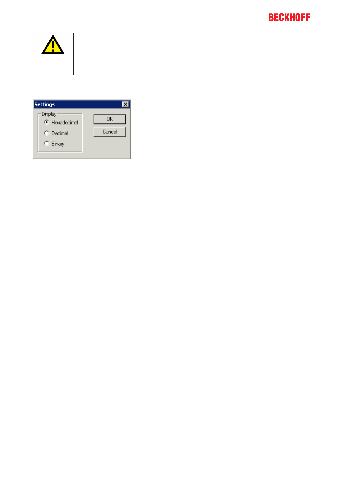
After pressing the Settings button you can set the format of the numerical display to hexadecimal, decimal or
binary.
Fig.30: Settings
application.
Only modify these initial values if you are certain that the state of your equipment permits it,
and that there will be no risk to people or to the machine!
KL2535, KL254536 Version: 2.0.0
Page 37
Access from the user program
5 Access from the user program
5.1 Process image
The KL2535 and KL2545 appear in the complex process image with at least 6 bytes of input and 6 bytes of
output data. These are organized as follows:
Byte offset (without word
alignment)
0 0 Byte
1 2 Word DataIN1 DataOUT1
3 4 Byte
4 6 Word DataIN2 DataOUT2
The KL2535 and KL2545 appear in the complex process image with at least 6 bytes of output data. These
are organized as follows:
Byte offset (without word
alignment)
0 0 Byte -
1 2 Word - DataOUT1
3 4 Byte -
4 6 Word - DataOUT2
*) Word alignment: The Bus Coupler places values on even byte addresses
Byte offset (with word alignment*)
Byte offset (with word alignment*)
Format Input data Output data
SB1 [}38] CB1 [}38]
SB2 [}39] CB2 [}39]
Format Input data Output data
CB1 [}38]
CB2 [}39]
Legend
SB n: status byte channel n
CB n: Control byte of channel n
DataIN n: Input word of channel n
DataOUT n: Output word of channel n
Process image
It is not possible for the KL2535 or KL2545 to operate without control bytes, since the con-
Note
trol bytes are required to enable the channels. Even if you adjust your bus coupler to the
compact process image, the KL2535 and KL2545 will still be represented with their control
bytes!
Process data
Output value Output current
-32767
0
dec
+32767
dec
dec
-100% of the maximum output current (see Register R36
[}43])
0
+100% of the maximum output current (see Register R36
[}43])
KL2535, KL2545 37Version: 2.0.0
Page 38
Access from the user program
5.2 Control and status bytes
Channel 1
Process data mode
Control byte 1 (for process data mode)
Control byte 1 (CB1) is located in the output image [}37], and is transmitted from the controller to the
terminal.
Bit CB1.7 CB1.6 CB1.5 CB1.4 CB1.3 CB1.2 CB1.1 CB1.0
Name RegAccess Reset Enable GetLatchDataenLatch
FallEdge
Legend
Bit Name Description
CB1.7 RegAccess 0
CB1.6 Reset 1
CB1.5 Enable 1
CB1.4 GetLatchData 0
CB1.3 enLatch
FallEdge
CB1.2 enLatch
RiseEdge
CB1.1 SetPos 1
CB1.0 enDithering 1
Register communication off (process data mode)
bin
all errors that may have occurred are reset by setting this bit (rising edge)
bin
Enables channel 1
bin
Show the current position in the input process data
bin
1
Show the current latch value in the input process data
bin
1
External latch event is enabled (for latch inputs with falling edge, the
bin
terminal saves the current position)
1
External latch event is enabled (for latch inputs with rising edge, the
bin
terminal saves the current position)
ATTENTION: Higher priority than CB1.3 !
Position value is set with register R1 [}41] (rising edge)
bin
Dithering is active (when R32.5 [}43]=1)
bin
enLatch
RiseEdge
SetPosenDithering
Status byte 1 (for process data mode)
The status byte 1 (SB1) is located in the input image [}37], and is transmitted from terminal to the controller.
Bit SB1.7 SB1.6 SB1.5 SB1.4 SB1.3 SB1.2 SB1.1 SB1.0
Name RegAccess Error Warning Ready LatchData LatchValid SetPos Ready Input E1
Legend
Bit Name Description
SB1.7 RegAccess 0
SB1.6 Error 1
SB1.5 Warning 1
SB1.4 Ready 0
SB1.3 LatchData 0
SB1.2 LatchValid 1
SB1.1 SetPos Ready 1
SB1.0 Input E1 Status of input E1
Acknowledgement for process data mode
bin
An error has occurred (is displayed in the status word in register R0)
bin
The internal temperature has risen to more than 80 ℃, or the power supply
bin
voltage has dropped.
Motor control is disabled or an error has occurred (SB.6=1)
bin
1
Motor control is enabled and no error has occurred (acknowledgement for
bin
enable, SB.6=0)
The current position is mapped into the input process data
bin
1
The most recent latch value is mapped into the process data, provided a
bin
valid latch value exists (acknowledgement for GetLatchData)
A latch event has occurred (when CB1.2=1 or CB1.3=1)
bin
The current position has been set (acknowledgement for SetPos)
bin
KL2535, KL254538 Version: 2.0.0
Page 39

Access from the user program
Register communication
Control byte 1 (in register communication)
Control byte 1 (CB1) is located in the output image [}37], and is transmitted from the controller to the
terminal.
Bit CB1.7 CB1.6 CB1.5 CB1.4 CB1.3 CB1.2 CB1.1 CB1.0
Name RegAccess R/W Reg. no.
Legend
Bit Name Description
CB1.7 RegAccess 1
CB1.6 R/W 0
CB1.5 to
Reg. no. Register number:
CB1.0
Register communication switched on
bin
Read access
bin
1
Write access
bin
Enter here the number of the register [}40] that you wish
- to read with input data word DataIn [}37], or
- to write with output data word DataOut [}37].
Status byte 1 (in register communication)
The status byte 1 (SB1) is located in the input image [}37], and is transmitted from terminal to the controller.
Bit SB1.7 SB1.6 SB1.5 SB1.4 SB1.3 SB1.2 SB1.1 SB1.0
Name RegAccess R/W Reg. no.
Legend
Bit Name Description
SB1.7 RegAccess 1
SB1.6 R 0
SB1.5 to
Reg. no. Number of the register that was read or written.
Acknowledgement for register access
bin
Read access
bin
SB1.0
Channel 2
The control and status bytes of channel 2 (CB2 and SB2) have the same structure as the control and status
bytes of channel 1.
KL2535, KL2545 39Version: 2.0.0
Page 40

Access from the user program
5.3 Register overview
The registers serve the parameterization of the pulse width current terminal. They can be read or written by
means of register communication.
Register no. Comment Default value R/W Memory
R0 [}41]
R1 [}41]
R2 [}41]
R3 [}41]
Status word 0x0000 0
Set position (only on the KL2545) 0x0000 0
Coil voltage (only on the KL2545) 0x0000 0
Power supply voltage (only on the
e.g. 0x0030 e.g. 48
dec
dec
dec
dec
KL2545)
R4 reserved - - - -
R5 [}41]
R6 [}41]
R7 [}42]
R8 [}42]
R9 [}42]
R10 Multiplex shift register 0x0130 304
R11 Signal channels 0x0218 536
R12 Minimum data length 0x1818 6168
R13 Data structure 0x0004 4
Temperature (only on the KL2545) e.g. 0x0023 e.g. 35
Status byte e.g. 0x0010 e.g. 16
Command register 0x0000 0
Terminal type KL2535: 0x09E7 2535
KL2545: 0x09F1 2545
dec
dec
dec
Firmware version e.g. 0x3141 e.g. 1A
dec
dec
dec
dec
dec
dec
ASCII
R14 reserved - - - -
R15 Alignment register 0x7F80 32640
R16 [}42]
Hardware version number e.g. 0x0000 e.g. 0
dec
dec
R17 reserved - - - -
... ... ... ... ... ...
R30 reserved - - - -
R31 [}43]
R32 [}43]
R33 [}43]
R34 [}43]
R35 [}43]
R36 [}43]
R37 [}44]
R38 [}44]
R39 [}44]
R40 [}44]
R41 [}44]
R42 [}44]
R43 [}44]
R44 [}44]
R45 [}44]
R46 [}45]
Code word register 0x0000 0
Feature register 0x0000 0
dec
dec
User scaling - offset 0x1000 4096
User scaling - gain 0x0000 0
User's switch-on value 0x0000 0
dec
dec
Maximum output current KL2535: 0x03E8 1000
KL2545: 0x0DAC 3500
Dithering - Frequency 0x0000 0
Dithering amplitude 0x0000 0
Dithering - Switch-off ramp 0x0000 0
Overlap threshold value 0x0000 0
Overlap output value 0x0000 0
Bend compensation -threshold value 0x0000 0
Bend compensation - output value 0x0000 0
dec
dec
dec
dec
dec
dec
dec
Area compensation - threshold value 0x03E8 1000
Process data ramp (rising) 0x0000 0
Process data ramp (falling) 0x0000 0
dec
dec
dec
dec
dec
dec
R47 reserved
R63 reserved
R RAM
R/W RAM
R RAM
R RAM
R RAM
R RAM
R/W RAM
R ROM
R ROM
R ROM
R ROM
R ROM
R ROM
R/W RAM
R/W EEPROM
R/W RAM
R/W EEPROM
R/W EEPROM
R/W EEPROM
R/W EEPROM
R/W EEPROM
R/W EEPROM
R/W EEPROM
R/W EEPROM
R/W EEPROM
R/W EEPROM
R/W EEPROM
R/W EEPROM
R/W EEPROM
R/W EEPROM
R/W EEPROM
KL2535, KL254540 Version: 2.0.0
Page 41

Access from the user program
5.4 Register description
All registers can be read or written via register communication. They are used for parameterizing the
terminal.
R0: Status word
The status word contains information about internal states, and provides an indication of errors that have
occurred.
Bit R0.15 R0.14 R0.13 R0.12 R0.11 R0.10 R0.9 R0.8
Name - NoControlPower OpenLoad OverCurrent UnderVoltage - LowVoltage OverTemperature
Bit R0.7 R0.6 R0.5 R0.4 R0.3 R0.2 R0.1 R0.0
Name - - - - - - - -
Legend
Bit Name Description
R0.15 - reserved
R0.14 NoControlPower 1
R0.13 OpenLoad 1
R0.12 OverCurrent 1
R0.11 UnderVoltage 1
bin
bin
bin
bin
R0.10 - reserved
R0.9 LowVoltage 1
R0.8 OverTemperature 1
bin
bin
R0.0-R0.7 - reserved
The 24 V control voltage is not present at the power contacts
Open load / broken wire
Overcurrent in the driver stage
Supply voltage less than 7 V (only on the KL2545)
The supply voltage is 10 V less than the switch-on voltage (only
on the KL2545)
The internal temperature of the terminal is greater than 80℃ (see
R5 [}41]) (only on the KL2545)
R1: Set position
You can specify the desired position, with which the terminal is to be loaded, here.
R2: Coil voltage
You can read the coil voltage here. The unit is 1 mV (for example: 4800 = 48V).
R3: Supply voltage
You can read the power supply voltage here. The unit is 1 mV (for example: 4800 = 48V).
R5: Temperature register
The internal temperature of the terminal can be read, in °C, through register R5. The terminal will set bit SB.5
[}38] in the status byte as a warning if the temperature exceeds the threshold of 80°C. When the
temperature falls back below 60°C, bit SB.5 [}38] will automatically be reset.
R6: Status byte
The status byte of the relevant channel is mapped here in addition.
KL2535, KL2545 41Version: 2.0.0
Page 42

Access from the user program
R7: Command register
User code word
For the following commands to be executed, it is first necessary for the user code word,
Note
0x1235, to be entered into register R31 [}43].
Command 0x7000: Restore Factory Settings
Entering 0x7000 in register R7 restores the factory settings for the following registers of both channels:
R32: 0
dec
R33: 0
dec
R34: 4096
R35: 0
R36: KL2535: 1000
R37: 0
R38: 0
R39: 0
R40: 0
R41: 0
R42: 0
R43: 0
R44: 1000
R45: 0
R46: 0
dec
dec
dec
dec
dec
dec
dec
dec
dec
dec
dec
dec
, KL2545: 3500
dec
dec
Complete restore
The Restore Factory Settings command resets both channels in the pulse-width current
terminal to the factory settings simultaneously, regardless of which register set it is called
Note
from!
Command 0x8000: Software Reset
Entering 0x8000 in register R7 initiates a full software reset for the terminal. All internal variables (positions,
latched values, errors etc.) are cleared or are set to defined values that are read from the EEPROM. The
internal circuits (D/A converter, output driver) are reinitialized during a software reset.
Software reset!
Power is removed from the output stage during a software reset. Ensure that your system
CAUTION
state permits this and that hazards for persons or machinery have been ruled out!
R8: Terminal type
The terminal identifier is contained in register R8:
KL2535: 0x09E7 (2535
KL2545: 0x09F1 (2545
dec
dec
)
)
R9: Firmware version
Register R9 contains the ASCII coding of the terminal's firmware version, e.g. 0x3141 = '1A'. The '0x31'
corresponds here to the ASCII character '1', while the '0x41' represents the ASCII character 'A'.
This value cannot be changed.
R16: Hardware version number
Register R16 contains the hardware version of the terminal.
KL2535, KL254542 Version: 2.0.0
Page 43

Access from the user program
R31: Code word register
If you write values into the user registers without first entering the user code word (0x1235) into the code
word register, the terminal will not accept the supplied data. The code word is reset if the terminal is
restarted.
R32: Feature register
The feature register specifies the terminal's configuration.
Bit R32.15 R32.14 R32.13 R32.12 R32.11 R32.10 R32.9 R32.8
Name disMixedDecay - - - - - - enUserStartValue
Bit R32.7 R32.6 R32.5 R32.4 R32.3 R32.2 R32.1 R32.0
Name - enRamps enDithering enValveCurve enAverageNotation disWatchdog enManuScale enUserScale
Legend
Bit Name Description default
R32.15 disMixedDecay 1
bin
R32.14-R32.9 - reserved
R32.8 enUserStartValue 1
bin
R32.7 - reserved
R32.6 enRamps 1
R32.5 enDithering 1
R32.4 enValveCurve 1
R32.3 enAverageNotation0
R32.2 disWatchdog 1
R32.1 enManuScale 1
R32.0 enUserScale 1
bin
bin
bin
bin
1
bin
bin
bin
bin
Mixed Decay is deactivated 0
User switch-on value active (see R35 [}43])
Process data ramps [}17] are active (see R45
[}44] + R46 [}45])
Dithering [}15] is active (see R37 [}44], R38
[}44] + R39 [}44]); bit CB1.0 [}38] = 1 must be
set in addition
Valve curve [}16] is active (see R40 [}44], R41
[}44], R42 [}44], R43 [}44] + R44 [}44])
Two’s complement representation is active 0
Signed amount representation active
Internal 100 ms watchdog deactivated 0
Manufacturer scaling is active 0
User scaling active (see R33 [}43]+ R34 [}43])
bin
0
bin
0
bin
0
bin
0
bin
bin
bin
bin
0
bin
R33: User scaling - offset
If user-scaling is active (R32.0 [}43]=1) this register specifies the offset for the user-scaling.
R34: User scaling - gain
If user-scaling is active (R32.0 [}43]=1) this register specifies the gain for the user-scaling.
R35: User's switch-on value
If the user switch-on value is active (R32.8 [}43]=1) and if the activated watchdog (R32.2 [}43]=0
triggers following a fieldbus or terminal bus error continuing for 100 ms, the output will be set to this value.
)
bin
R36: Maximum output current
This register specifies the maximum output current. The unit is 1 mA (for example: 1000
KL2535: maximum 1000mA (default: 1000
KL2545: maximum 3500mA (default: 3500
dec
dec
)
)
KL2535, KL2545 43Version: 2.0.0
= 1 A).
dec
Page 44

Access from the user program
R37: Dithering - Frequency
When Dithering [}15] is active (R32.5 [}43]=1) this register specifies the frequency of the dither.
Values from 10 to 500 Hz are permitted.
The unit is 1 Hz. (Example: 100
= 100 Hz).
dec
R38: Dithering amplitude
When Dithering [}15] is active (R32.5 [}43]=1) this register specifies the amplitude of the dither.
The configured value refers to the set output current in register R36 [}43].
The unit is 1% (for example: 10
= 10%).
dec
R39: Dithering - Switch-off ramp
When Dithering [}15] is active (R32.5 [}43]=1) this register specifies the switch-off ramp of the dither.
The unit is 1 ms (for example: 100
= 100 ms).
dec
R40: Overlap - Threshold value (valve curve)
When the valve curve [}16] is active (R32.4 [}43]=1) this register specifies the threshold value for the
overlap region.
The unit is 0.1%, and is expressed with reference to the final process data value (for example: 100
dec
= 10%).
R41: Overlap - Output value (valve curve)
When the valve curve [}16] is active (R32.4 [}43]=1) this register specifies the output value for the overlap
region.
The configured value refers to the set output current in register R36 [}43].
The unit is 0.1% (for example: 100
= 10%).
dec
R42: Bend compensation - Threshold value (valve curve)
When the valve curve [}16] is active (R32.4 [}43]=1) this register specifies the threshold value for the bend
compensation region.
The unit is 0.1%, and is expressed with reference to the final process data value (for example: 100
= 10%).
dec
R43: Bend compensation - Output value (valve curve)
When the valve curve [}16] is active (R32.4 [}43]=1) this register specifies the output value for the bend
compensation region.
The configured value refers to the set output current in register R36 [}43].
The unit is 0.1% (for example: 100
= 10%).
dec
R44: Area compensation - Threshold value (valve curve)
When the valve curve [}16] is active (R32.4 [}43]=1) this register specifies the threshold value for the area
compensation region.
The unit is 0.1%, and is expressed with reference to the final process data value (for example: 100
= 10%).
dec
R45: Process data ramp (rising)
When the process data ramps are active (R32.6 [}43]=1), this register specifies the rising process data ramp
[}17].
The unit is 1 ms, and is expressed with reference to the final process data value (for example: 100
ms).
KL2535, KL254544 Version: 2.0.0
= 100
dec
Page 45

Access from the user program
R46: Process data ramp (falling)
When the process data ramps are active (R32.6 [}43]=1), this register specifies the falling process data ramp
[}17].
The unit is 1 ms, and is expressed with reference to the final process data value (for example: 100
ms).
= 100
dec
5.5 Examples of Register Communication
The numbering of the bytes in the examples corresponds to the display without word alignment.
5.5.1 Example 1: reading the firmware version from Register 9 of a terminal
Byte 0: Control byte Byte 1: DataOUT1, high byte Byte 2: DataOUT1, low byte
0x89 (1000 1001
Explanation:
) 0xXX 0xXX
bin
• Bit 0.7 set means: Register communication switched on.
• Bit 0.6 not set means: reading the register.
• Bits 0.5 to 0.0 specify the register number 9 with 00 1001
• The output data word (byte 1 and byte 2) has no meaning during read access. To change a register,
write the required value into the output word.
Byte 0: Status byte Byte 1: DataIN1, high byte Byte 2: DataIN1, low byte
0x89 0x33 0x41
Explanation:
• The terminal returns the value of the control byte as a receipt in the status byte.
• The terminal returns the firmware version 0x3341 in the input data word (byte 1 and byte 2). This is to
be interpreted as an ASCII code:
◦ ASCII code 0x33 represents the digit 3
◦ ASCII code 0x41 represents the letter A
The firmware version is thus 3A.
.
bin
5.5.2 Example 2: Writing to a user register
Code word
In normal mode all user registers are read-only with the exception of Register 31. In order
Note
to deactivate this write protection you must write the code word (0x1235) into Register 31. If
a value other than 0x1235 is written into Register 31, write protection is reactivated. Please
note that changes to a register only become effective after restarting the terminal (poweroff/power-on).
I. Write the code word (0x1235) into Register 31.
Byte 0: Control byte Byte 1: DataOUT1, high byte Byte 2: DataOUT1, low byte
0xDF (1101 1111
Explanation:
• Bit 0.7 set means: Register communication switched on.
KL2535, KL2545 45Version: 2.0.0
) 0x12 0x35
bin
Page 46

Access from the user program
• Bit 0.6 set means: writing to the register.
• Bits 0.5 to 0.0 specify the register number 31 with 01 1111
.
bin
• The output data word (byte 1 and byte 2) contains the code word (0x1235) for deactivating write
protection.
Byte 0: Status byte Byte 1: DataIN1, high byte Byte 2: DataIN1, low byte
0x9F (1001 1111
) 0xXX 0xXX
bin
Explanation:
• The terminal returns a value as a receipt in the status byte that differs only in bit 0.6 from the value of
the control byte.
• The input data word (byte 1 and byte 2) is of no importance after the write access. Any values still
displayed are invalid!
II. Read Register 31 (check the set code word)
Byte 0: Control byte Byte 1: DataOUT1, high byte Byte 2: DataOUT1, low byte
0x9F (1001 1111
Explanation:
) 0xXX 0xXX
bin
• Bit 0.7 set means: Register communication switched on.
• Bit 0.6 not set means: reading the register.
• Bits 0.5 to 0.0 specify the register number 31 with 01 1111
.
bin
• The output data word (byte 1 and byte 2) has no meaning during read access.
Byte 0: Status byte Byte 1: DataIN1, high byte Byte 2: DataIN1, low byte
0x9F (1001 1111
) 0x12 0x35
bin
Explanation:
• The terminal returns the value of the control byte as a receipt in the status byte.
• The terminal returns the current value of the code word register in the input data word (byte 1 and byte
2).
III. Write to Register 32 (change contents of the feature register)
Byte 0: Control byte Byte 1: DataIN1, high byte Byte 2: DataIN1, low byte
0xE0 (1110 0000
Explanation:
• Bit 0.7 set means: Register communication switched on.
• Bit 0.6 set means: writing to the register.
• Bits 0.5 to 0.0 indicate register number 32 with 10 0000
• The output data word (byte 1 and byte 2) contains the new value for the feature register.
CAUTION
) 0x00 0x02
bin
.
bin
Observe the register description!
The value of 0x0002 given here is just an example! The bits of the feature register change
the properties of the terminal and have a different meaning, depending on the type of terminal. Refer to the description of the feature register of your terminal (chapter "Register description") regarding the meaning of the individual bits before changing the values.
Byte 0: Status byte Byte 1: DataIN1, high byte Byte 2: DataIN1, low byte
0xA0 (1010 0000
) 0xXX 0xXX
bin
KL2535, KL254546 Version: 2.0.0
Page 47

Access from the user program
Explanation:
• The terminal returns a value as a receipt in the status byte that differs only in bit 0.6 from the value of
the control byte.
• The input data word (byte 1 and byte 2) is of no importance after the write access. Any values still
displayed are invalid!
IV. Read Register 32 (check changed feature register)
Byte 0: Control byte Byte 1: DataOUT1, high byte Byte 2: DataOUT1, low byte
0xA0 (1010 0000
Explanation:
• Bit 0.7 set means: Register communication switched on.
• Bit 0.6 not set means: reading the register.
• Bits 0.5 to 0.0 indicate register number 32 with 10 0000
• The output data word (byte 1 and byte 2) has no meaning during read access.
Byte 0: Status byte Byte 1: DataIN1, high byte Byte 2: DataIN1, low byte
0xA0 (1010 0000
) 0xXX 0xXX
bin
.
bin
) 0x00 0x02
bin
Explanation:
• The terminal returns the value of the control byte as a receipt in the status byte.
• The terminal returns the current value of the feature register in the input data word (byte 1 and byte 2).
V. Write Register 31 (reset code word)
Byte 0: Control byte Byte 1: DataOUT1, high byte Byte 2: DataOUT1, low byte
0xDF (1101 1111
Explanation:
• Bit 0.7 set means: Register communication switched on.
• Bit 0.6 set means: writing to the register.
• Bits 0.5 to 0.0 specify the register number 31 with 01 1111
• The output data word (byte 1 and byte 2) contains 0x0000 for reactivating write protection.
Byte 0: Status byte Byte 1: DataIN1, high byte Byte 2: DataIN1, low byte
0x9F (1001 1111
Explanation:
• The terminal returns a value as a receipt in the status byte that differs only in bit 0.6 from the value of
the control byte.
• The input data word (byte 1 and byte 2) is of no importance after the write access. Any values still
displayed are invalid!
) 0x00 0x00
bin
.
bin
) 0xXX 0xXX
bin
KL2535, KL2545 47Version: 2.0.0
Page 48

Appendix
6 Appendix
6.1 Support and Service
Beckhoff and their partners around the world offer comprehensive support and service, making available fast
and competent assistance with all questions related to Beckhoff products and system solutions.
Beckhoff's branch offices and representatives
Please contact your Beckhoff branch office or representative for local support and service on Beckhoff
products!
The addresses of Beckhoff's branch offices and representatives round the world can be found on her internet
pages:
http://www.beckhoff.com
You will also find further documentation for Beckhoff components there.
Beckhoff Headquarters
Beckhoff Automation GmbH & Co. KG
Huelshorstweg 20
33415 Verl
Germany
Phone: +49(0)5246/963-0
Fax: +49(0)5246/963-198
e-mail: info@beckhoff.com
Beckhoff Support
Support offers you comprehensive technical assistance, helping you not only with the application of
individual Beckhoff products, but also with other, wide-ranging services:
• support
• design, programming and commissioning of complex automation systems
• and extensive training program for Beckhoff system components
Hotline: +49(0)5246/963-157
Fax: +49(0)5246/963-9157
e-mail: support@beckhoff.com
Beckhoff Service
The Beckhoff Service Center supports you in all matters of after-sales service:
• on-site service
• repair service
• spare parts service
• hotline service
Hotline: +49(0)5246/963-460
Fax: +49(0)5246/963-479
e-mail: service@beckhoff.com
KL2535, KL254548 Version: 2.0.0
Page 49

List of illustrations
List of illustrations
Fig. 1 KL2535 ...................................................................................................................................... 7
Fig. 2 KL2535 - LEDs .......................................................................................................................... 9
Fig. 3 KL2545 ...................................................................................................................................... 10
Fig. 4 KL2545 - LEDs .......................................................................................................................... 12
Fig. 5 Operation at load with adequate inductance ............................................................................. 13
Fig. 6 Operation at load inadequate inductance (near ohmic)............................................................. 13
Fig. 7 Frequency - f / Amplitude - i....................................................................................................... 15
Fig. 8 Switch-off ramp - t...................................................................................................................... 16
Fig. 9 Valve curve ................................................................................................................................ 17
Fig. 10 Process data ramps ................................................................................................................... 17
Fig. 11 Attaching on mounting rail ......................................................................................................... 18
Fig. 12 Disassembling of terminal.......................................................................................................... 19
Fig. 13 Power contact on left side.......................................................................................................... 20
Fig. 14 Recommended distances for standard installation position ...................................................... 21
Fig. 15 Standard wiring .......................................................................................................................... 22
Fig. 16 Pluggable wiring ........................................................................................................................ 22
Fig. 17 High Density Terminals.............................................................................................................. 22
Fig. 18 Mounting a cable on a terminal connection ............................................................................... 23
Fig. 19 KL2535 Connection ................................................................................................................... 25
Fig. 20 KL2545 Connection ................................................................................................................... 26
Fig. 21 KS2000 configuration software .................................................................................................. 28
Fig. 22 Display of the fieldbus station in KS2000 .................................................................................. 30
Fig. 23 KS2000 tree branches for channel 1 of the KL2535 .................................................................. 30
Fig. 24 Settings via KS2000 .................................................................................................................. 31
Fig. 25 Register view in KS2000............................................................................................................ 34
Fig. 26 ProcData .................................................................................................................................... 35
Fig. 27 History field ................................................................................................................................ 35
Fig. 28 Value field .................................................................................................................................. 35
Fig. 29 Value field .................................................................................................................................. 35
Fig. 30 Settings ...................................................................................................................................... 36
KL2535, KL2545 49Version: 2.0.0
 Loading...