

Page 1

BDTIC www.bdtic.com/ATMEL
Features
• High Performance, Low Power AVR
• Advanced RISC Architecture
– 130 Powe rful Instructions – Most Single Clock Cy cle Execution
– 32 x 8 General Purpose Working Registers
– Fully Static Operation
– Up to 16 MIPS Throughput at 16 MHz
– On-Chip 2-cycle Multiplier
• High Endurance Non-volatile Memory Segments
– In-System Self-programmable Flash Program Memory
• 32K Bytes (ATmega325/ATmega3250)
• 64K Bytes (ATmega645/ATmega6450)
– EEPROM
• 1K bytes (ATmega325/ATmega3250)
• 2K bytes (ATmega645/ATmega6450)
– Internal SRAM
• 2K bytes (ATmega325/ATmega3250)
• 4K bytes (ATmega645/ATmega6450)
– Write/Erase Cycles: 10,000 Flash/ 100,000 EEPROM
– Data retention: 20 years at 85°C/100 years at 25°C
– Optional Boot Code Section with Independent Lock Bits
• In-System Programming by On-chip Boot Program
• True Read-While-Write Operation
– Programming Lock for Software Security
• JTAG (IEEE std. 1149.1 compliant) Interface
– Boundary-scan Capabilities According to the JTAG Standard
– Extensive On-chip Debug Support
– Programming of Flash, EEPROM, Fuses, and Lock Bits through the JTAG Interface
• Peripheral Features
– Two 8-bit Timer/Counters with Separate Prescaler and Compare Mode
– One 16-bit Timer/Counter with Separate Prescaler, Compare Mode, and Capture
Mode
– Real Time Counter with Separate Oscillator
–Four PWM Channels
– 8-channel, 10-bit ADC
– Programmable Serial USART
– Master/Slave SPI Serial Interface
– Universal Serial Interface with Start Condition Detector
– Programmable Watchdog Timer with Separate On-chip Oscillator
– On-chip Analog Comparator
– Interrupt and Wake-up on Pin Change
• Special Microcontroller Features
– Power-on Reset and Pr ogrammab l e Brown-out Detection
– Internal Calibrated Oscillator
– External and Internal Interrupt Sources
– Five Sleep Modes: Idle, ADC Noise Reduction, Power-save, Power-down, and
Standby
• I/O and Pac kages
– 53/68 Programmable I/O Lines
– 64-lead TQFP, 64-pad QFN/MLF, and 100-lead TQFP
• Speed Grade:
– ATmega325V/ATmega3250V/ATmega645V/ATmega6450V:
• 0 - 4 MHz @ 1.8 - 5.5V, 0 - 8 MHz @ 2.7 - 5.5V
– ATmega325/3250/645/6450:
• 0 - 8 MHz @ 2.7 - 5.5V, 0 - 16 MHz @ 4.5 - 5.5V
• Temperature range:
– -40°C to 85°C Industrial
• Ultra-Low Power Consumption
– Active Mode:
1 MHz, 1.8V: 350 µA
32 kHz, 1.8V: 20 µA (including Oscillator)
– Power-down Mode:
100 nA at 1.8V
®
8-Bit Microcontroller
(1)
8-bit
Microcontroller
with In-System
Programmable
Flash
ATmega325/V
ATmega3250/V
ATmega645/V
ATmega6450/V
Preliminary
Summary
Page 2
ATmega325/3250/645/6450
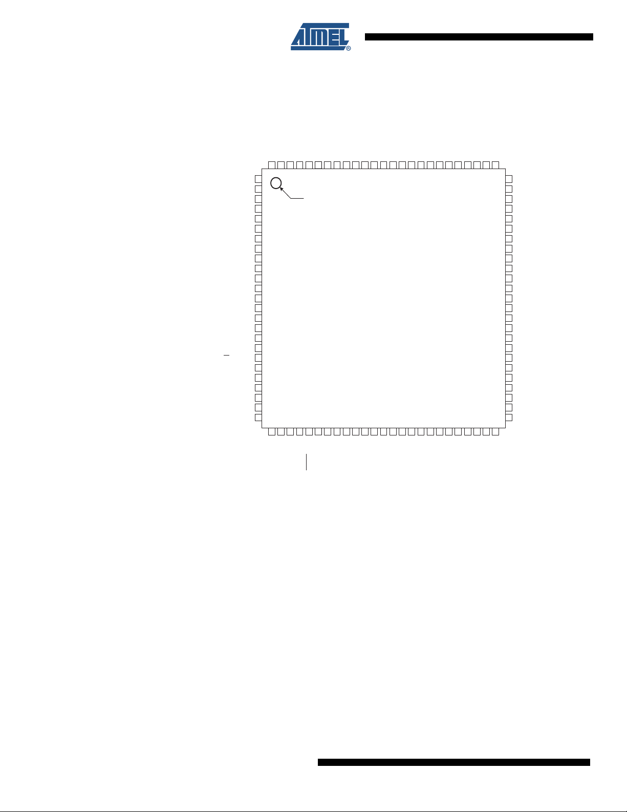
1. Pin Configurations
Figure 1-1. Pinout ATmega3250/6450
(RXD/PCINT0) PE0
DNC
(TXD/PCINT1) PE1
(XCK/AIN0/PCINT2) PE2
(AIN1/PCINT3) PE3
(USCK/SCL/PCINT4) PE4
(DI/SDA/PCINT5) PE5
(DO/PCINT6) PE6
(CLKO/PCINT7) PE7
VCC
GND
DNC
(PCINT24) PJ0
(PCINT25) PJ1
DNC
DNC
DNC
DNC
(SS/PCINT8) PB0
(SCK/PCINT9) PB1
(MOSI/PCINT10) PB2
(MISO/PCINT11) PB3
(OC0A/PCINT12) PB4
(OC1A/PCINT13) PB5
(OC1B/PCINT14) PB6
AVCC
AGND
AREF
PF0 (ADC0)
PF1(ADC1)
PF2 (ADC2)
PF3 (ADC3)
PF4 (ADC4/TCK)
PF5 (ADC5/TMS)
PF6 (ADC6/TDO)
PF7 (ADC7/TDI)
DNC
DNC
PH7 (PCINT23)
PH6 (PCINT22)
PH5 (PCINT21)
PH4 (PCINT20)
DNC
DNC
GND
9998979695949392919089888786858483828180797877
100
1
2
3
4
5
6
7
8
9
10
11
12
13
14
15
16
17
18
19
20
21
22
23
24
25
26272829303132333435363738394041424344454647484950
INDEX CORNER
ATmega3250/6450
VCC
DNC
PA0
PA1
PA2
76
75
PA3
74
PA4
73
PA5
72
PA6
71
PA7
70
PG2
69
PC7
68
PC6
67
DNC
66
PH3 (PCINT19)
65
PH2 (PCINT18)
64
PH1 (PCINT17)
63
PH0 (PCINT16)
62
DNC
61
DNC
60
DNC
59
DNC
58
PC5
57
PC4
56
PC3
55
PC2
54
PC1
53
PC0
52
PG1
51
PG0
DNC
(T1) PG3
(T0) PG4
RESET/PG5
(OC2A/PCINT15) PB7
VCC
GND
XTAL2 (TOSC2)
XTAL1 (TOSC1)
DNC
DNC
(PCINT26) PJ2
(PCINT27) PJ3
(PCINT28) PJ4
(PCINT29) PJ5
DNC
(ICP1) PD0
(PCINT30) PJ6
PD2
(INT0) PD1
PD3
PD4
PD5
PD6
PD7
2
2570LS–AVR–08/07
Page 3
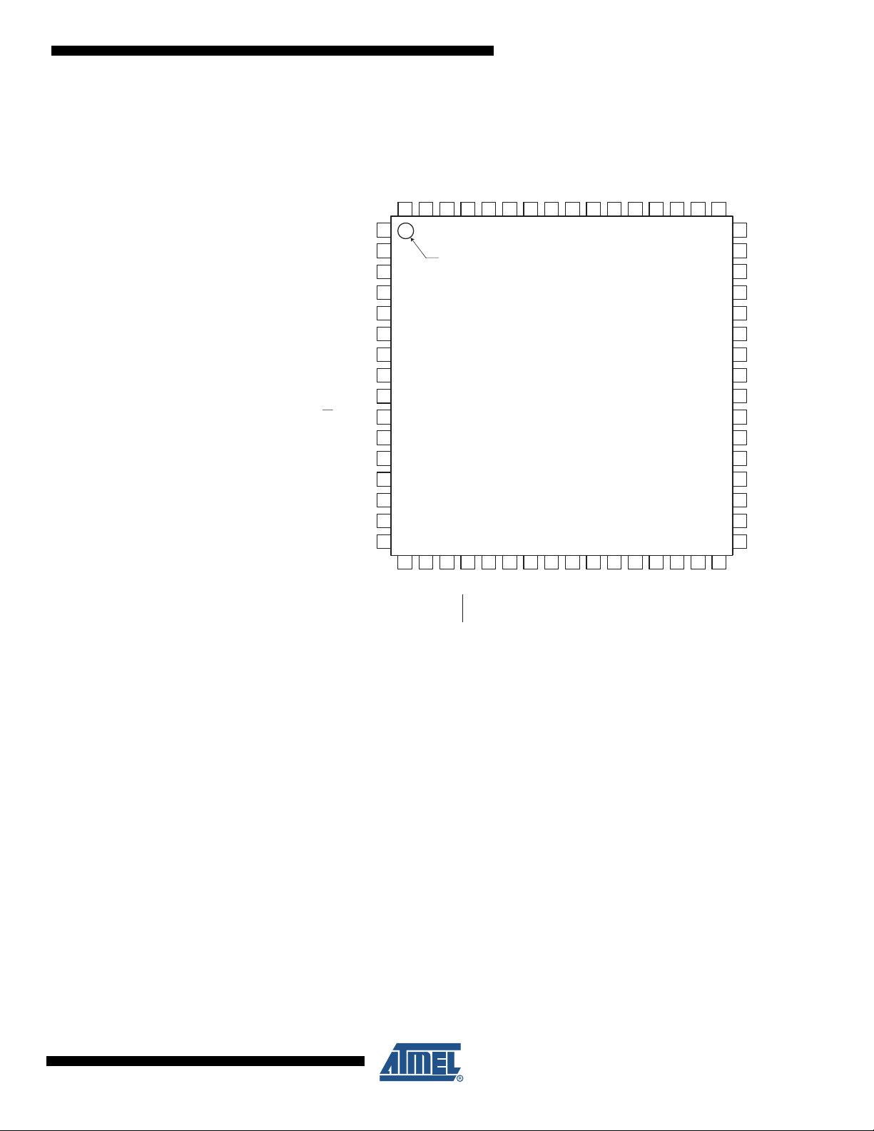
Figure 1-2. Pinout ATmega325/645
GND
AVCC
64
63
DNC
1
(RXD/PCINT0) PE0
(TXD/PCINT1) PE1
(XCK/AIN0/PCINT2) PE2
(AIN1/PCINT3) PE3
(USCK/SCL/PCINT4) PE4
(DI/SDA/PCINT5) PE5
(DO/PCINT6) PE6
(CLKO/PCINT7) PE7
(SS/PCINT8) PB0
(SCK/PCINT9) PB1
(MOSI/PCINT10) PB2
(MISO/PCINT11) PB3
(OC0A/PCINT12) PB4
(OC1A/PCINT13) PB5
(OC1B/PCINT14) PB6
2
3
4
5
6
7
8
9
10
11
12
13
14
15
16
17
(OC2A/PCINT15) PB7
INDEX CORNER
(T1) PG3
PF0 (ADC0)
AREF
61
62
19
(T0) PG4
RESET/PG5
ATmega325/3250/645/6450
VCC
GND
PF1 (ADC1)
PF2 (ADC2)
PF3 (ADC3)
6018592058
ATmega325/645
21
VCC
GND
XTAL2 (TOSC2)
PF4 (ADC4/TCK)
57225623552454255326522751
XTAL1 (TOSC1)
PF7 (ADC7/TDI)
PF5 (ADC5/TMS)
PF6 (ADC6/TDO)
PD2
PD1 (INT0)
(ICP1) PD0
28
PD3
29
PD4
PA0
30
PD5
PA1
50
31
PD6
PA2
49
32
PD7
48
47
46
45
44
43
42
41
40
39
38
37
36
35
34
33
PA3
PA4
PA5
PA6
PA7
PG2
PC7
PC6
PC5
PC4
PC3
PC2
PC1
PC0
PG1
PG0
2. Disclaimer
3. Overview
2570LS–AVR–08/07
Note: The large center pad underneath the QFN/MLF packages is made of metal and inter nally con-
nected to GND. It should be soldered or glued to the board to ensure good mechanical stability. If
the center pad is left unconnected, the package might loosen from the board.
Typical values contained in this datasheet are based on simulations and characterization of
other AVR microcontrollers manufactured o n th e same proce ss te ch nolo gy. Min a nd Ma x valu es
will be available after the device is characterized.
The ATmega325/3250/645/6450 is a low-power CMOS 8-bit microcontroller based on the AVR
enhanced RISC architecture. By executing powerful instructions in a single clock cycle, the
ATmega325/3250/645/6450 achieves through puts approaching 1 MIPS per MHz a llowing the
system designer to optimize power consumption versus processing speed.
3
Page 4
ATmega325/3250/645/6450
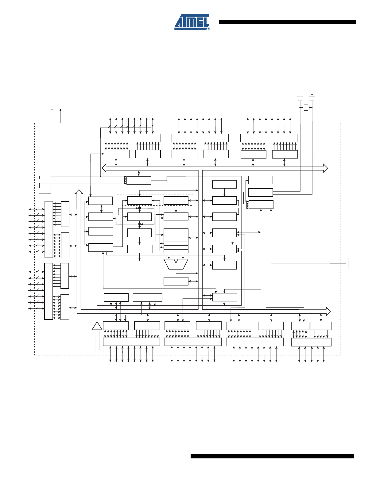
3.1 Block Diagram
Figure 3-1. Block Diagram
AVCC
AGND
AREF
PH0 - PH7
PORTH DRIVERS
VCCGND
DATA DIR.
REG. PORTH
PORTH
DATA REGISTER
DATA DIR.
REG. PORTJ
DATA REGISTER
JTAG TAP
ON-CHIP DEBUG
BOUNDARY-
SCAN
PROGRAMMING
LOGIC
PORTF
AVR CPU
PORTF DRIVERS
ADC
PROGRAM
COUNTER
PROGRAM
FLASH
INSTRUCTION
REGISTER
INSTRUCTION
DECODER
CONTROL
LINES
DATA DIR.
REG. PORTF
DATA REGISTER
PORTA
STACK
POINTER
SRAM
GENERAL
PURPOSE
REGISTERS
X
Y
Z
ALU
STATUS
REGISTER
PA0 - PA7PF0 - PF7
PORTA DRIVERS
DATA DIR.
REG. PORTA
8-BIT DATA BUS
INTERNAL
OSCILLATOR
WATCHDOG
TIMER
MCU CONTROL
REGISTER
TIMER/
COUNTERS
INTERRUPT
UNIT
EEPROM
PORTC DRIVERS
DATA REGISTER
PORTC
CALIB. OSC
OSCILLATOR
TIMING AND
CONTROL
PC0 - PC7
DATA DIR.
REG. PORTC
XTAL1
XTAL2
RESET
4
PJ0 - PJ6
PORTJ DRIVERS
PORTJ
DATA REGISTER
ANALOG
COMPARATOR
DATA REGISTER
+
-
USART
PORTE
UNIVERSAL
SERIAL INTERFACE
REG. PORTE
PORTE DRIVERS
DATA DIR.
DATA REGISTER
PORTB
PORTB DRIVERS
DATA DIR.
REG. PORTB
PB0 - PB7PE0 - PE7
SPI
DATAREGISTER
PORTD
PORTD DRIVERS
PD0 - PD7
DATA DIR.
REG. PORTD
DATAREG.
PORTG
PORTG DRIVERS
DATA DIR.
REG. PORTG
PG0 - PG4
The AVR core combines a rich instruction set with 32 general purpose working registers. All the
32 registers are directly connected to the Arithmetic Logic Unit (ALU), allowing two independent
registers to be accessed in one single instruction executed in one clock cycle. The resulting
architecture is more code efficient while achieving throughputs up to ten times faster than conventional CISC microcontrollers.
2570LS–AVR–08/07
Page 5
ATmega325/3250/645/6450
The ATmega325/3250/645/6450 provides the following features: 32/64K bytes of In-System
Programmable Flash with Read-While-Write capabilities, 1/2K bytes EEPROM, 2/4K byte
SRAM, 54/69 general purpose I/O lines, 32 general purpose working registers, a JTAG interface
for Boundary-scan, On-chip Debugging sup port an d pro gramming, three flexib le Timer /Co unters
with compare modes, internal and external interrupts, a serial programmable USART, Universal
Serial Interface with Start Condition Detector, an 8-channel, 10-bit ADC, a programmable
Watchdog Timer with internal Oscillator, an SPI serial port, and five software selectable power
saving modes. The Idle mode stops the CPU while allowing the SRAM, Timer/Counters, SPI
port, and interrupt system to continue functioning. The Power-down mode saves the register
contents but freezes the Oscillator, disabling all other chip functions until the next interrupt or
hardware reset. In Power-save mode, the asynchronous timer will continue to run, allowing the
user to maintain a timer base while the rest of the device is sleeping. The ADC Noise Reduction
mode stops the CPU and all I/O modules except asynchron ous timer and ADC to minimize
switching noise during ADC conversions. In Standby mode, the crystal/resonator Oscillator is
running while the rest of the device is sle eping. This allows very fast start-up combined with lowpower consumption.
The device is manufactured using Atmel’s high density non-volatile memory technology. The
On-chip In-System re-Programmable (ISP) Flash allows the program memory to be reprogrammed In-System through an SPI serial interface, by a conventional non-volatile memory
programmer, or by an On-chip Boot program running on the AVR core. The Bo ot program can
use any interface to download the application program in the Application Flash memory. Software in the Boot Flash section will continue to run while the Application Flash section is updated,
providing true Read-While-Write operation. By combining an 8-bit RISC CPU with In-System
Self-Programmable Flash on a monolithic chip, the Atmel ATmega325/3250/645/6450 is a powerful microcontroller that provides a highly flexible and cost effective solut ion to many embed ded
control applications.
The ATmega325/3250/645/6450 AVR is supported with a full suite of program and system
development tools including: C Compilers, Macro Assemblers, Program Debugger/Simulators,
In-Circuit Emulators, and Evaluation kits.
3.2 Comparison between ATmega325, ATmega3250, ATmega645 and ATmega6450
The ATmega325, ATmega3250, ATmega645, and ATmega6450 differs only in memory sizes,
pin count and pinout. Table 3-1 on page 5 summarizes the different configurations for the four
devices.
Table 3-1. Configuration Summary
General Purpose
Device Flash EEPROM RAM
ATmega325 32K bytes 1K bytes 2K bytes 54
ATmega3250 32K bytes 1K bytes 2K bytes 69
ATmega645 64K bytes 2K bytes 4K bytes 54
ATmega6450 64K bytes 2K bytes 4K bytes 69
I/O Pins
3.3 Pin Descriptions
The following section describes the I/O-pin special funct ion s.
2570LS–AVR–08/07
5
Page 6

ATmega325/3250/645/6450
3.3.1 V
3.3.2 GND
3.3.3 Port A (PA7..PA0)
3.3.4 Port B (PB7..PB0)
CC
Digital supply voltage.
Ground.
Port A is an 8-bit bi-directional I/O port with internal pull-up resistors (selected for each bit). The
Port A output buffers have symmetrical drive characteristics with both high sink and source
capability. As inputs, Port A pins that are externally pulled low will source current if the pull-up
resistors are activated. The Port A pins are tri-stated when a reset co ndition becomes active,
even if the clock is not running.
Port B is an 8-bit bi-directional I/O port with internal pull-up resistors (selected for each bit). The
Port B output buffers have symmetrical drive characteristics with both high sink and source
capability. As inputs, Port B pins that are externally pulled low will source current if the pull-up
resistors are activated. The Port B pins are tri-stated when a reset co ndition becomes active,
even if the clock is not running.
Port B has better driving capabilities than the other ports.
Port B also serves the function s of various special features of the ATmega325/3250/645/6450
as listed on page 67.
3.3.5 Port C (PC7..PC0)
Port C is an 8-bit bi-directional I/O port with internal pull-up resistors (selected for each bit). The
Port C output buffers have symmetrical drive characteristics with both high sink and source
capability. As inputs, Port C pins that are externally pulled low will source current if the pull-up
resistors are activated. The Port C pins are tri-stated when a reset condition becomes active,
even if the clock is not running.
3.3.6 Port D (PD7..PD0)
Port D is an 8-bit bi-directional I/O port with internal pull-up resistors (selected for each bit). The
Port D output buffers have symmetrical drive characteristics with both high sink and source
capability. As inputs, Port D pins that are externally pulled low will source current if the pull-up
resistors are activated. The Port D pins are tri-stated when a reset condition becomes active,
even if the clock is not running.
Port D also serves the functions of various special features of the ATmega325/3250/645/6450
as listed on page 70.
3.3.7 Port E (PE7..PE0)
Port E is an 8-bit bi-directional I/O port with internal pull-up resistors (selected for each bit). The
Port E output buffers have symmetrical drive characteristics with both high sink and source
capability. As inputs, Port E pins that are externally pulled low will source current if the pull-up
resistors are activated. The Port E pins are tri-stated when a reset co ndition becomes active,
even if the clock is not running.
Port E also serves the function s of various special features of the ATmega325/3250/645/6450
as listed on page 71.
6
2570LS–AVR–08/07
Page 7

3.3.8 Port F (PF7..PF0)
Port F serves as the analog inputs to the A/D Converter.
Port F also serves as an 8-bit bi-directional I/O port, if the A/D Converter is not used. Port pins
can provide internal pull-up resistors (selected for each bit) . The Por t F outpu t buffers ha ve symmetrical drive characteristics with both high sink and source capability. As inputs, Port F pins
that are externally pulled low will source current if the pull-up resistors are activated. The Port F
pins are tri-stated when a res et cond ition beco mes a ctive, ev en if th e clock is not ru nning. If the
JTAG interface is enabled, the pull-up resistors on pins PF7(TDI), PF5(TMS), and PF4(TCK) will
be activated even if a reset occurs.
Port F also serves the functions of the JTAG interface.
3.3.9 Port G (PG5..PG0)
Port G is a 6-bit bi-directional I/O port with internal pull-up resistors (selected for each bit). The
Port G output buffers have symmetrical drive characteristics with both high sink and source
capability. As inputs, Port G pins that are externally pulled low will source current if the pull-up
resistors are activated. The Port G pins are tri-stated when a reset condition becomes active,
even if the clock is not running.
Port G also serves the functions of various specia l features of the ATmega3 25/3250/645/6450
as listed on page 71.
ATmega325/3250/645/6450
3.3.10 Port H (PH7..PH0)
Port H is a 8-bit bi-directional I/O port with internal pull-up resistors (selected for each bit). The
Port H output buffers have symmetrical drive characteristics with both high sink and source
capability. As inputs, Port H pins that are externally pulled low will source current if the pull-up
resistors are activated. The Port H pins are tri-stated when a reset condition becomes active,
even if the clock is not running.
Port H also serves the functions of various special features of the ATmega3250/6450 as listed
on page 71.
3.3.11 Port J (PJ6..PJ0)
Port J is a 7-bit bi-directional I/O port with internal pull-up re sistors (selected for each bit). The
Port J output buffers have symmetrical drive characteristics with both high sink and source capability. As inputs, Port J pins that are externally pulled low will source current if the pull-up
resistors are activated. The Port J pins are tri-stated when a reset condition becomes active,
even if the clock is not running.
Port J also serves the functions of various special features of the ATmega3250/64 50 as listed on
page 71.
3.3.12 RESET
Reset input. A low level on this pin for longer than the minimum pulse length will generate a
reset, even if the clock is not running. The minimum pulse length is given in Table 28-4 on page
300. Shorter pulses are not guaranteed to gener at e a re se t.
3.3.13 XTAL1
2570LS–AVR–08/07
Input to the inverting Oscillator amplifier and input to the internal clock operating circuit.
7
Page 8

ATmega325/3250/645/6450
3.3.14 XTAL2
3.3.15 AVCC
3.3.16 AREF
4. Resources
5. Data Retention
Output from the inverting Oscillator amplifier.
AVCC is the supply voltage pin for Port F and the A/D Converter. It should be externally connected to V
through a low-pass filter.
This is the analog reference pin for the A/D Converter.
A comprehensive set of development tools, application notes and datasheets are available for
download on http://www.atmel.com/avr.
Note: 1.
Reliability Qualification results show that the projected data retention failure rate is much less
than 1 PPM over 20 years at 85°C or 100 years at 25°C.
, even if the ADC is not used. If the ADC is used, it should be connected to V
CC
CC
8
2570LS–AVR–08/07
Page 9
ATmega325/3250/645/6450
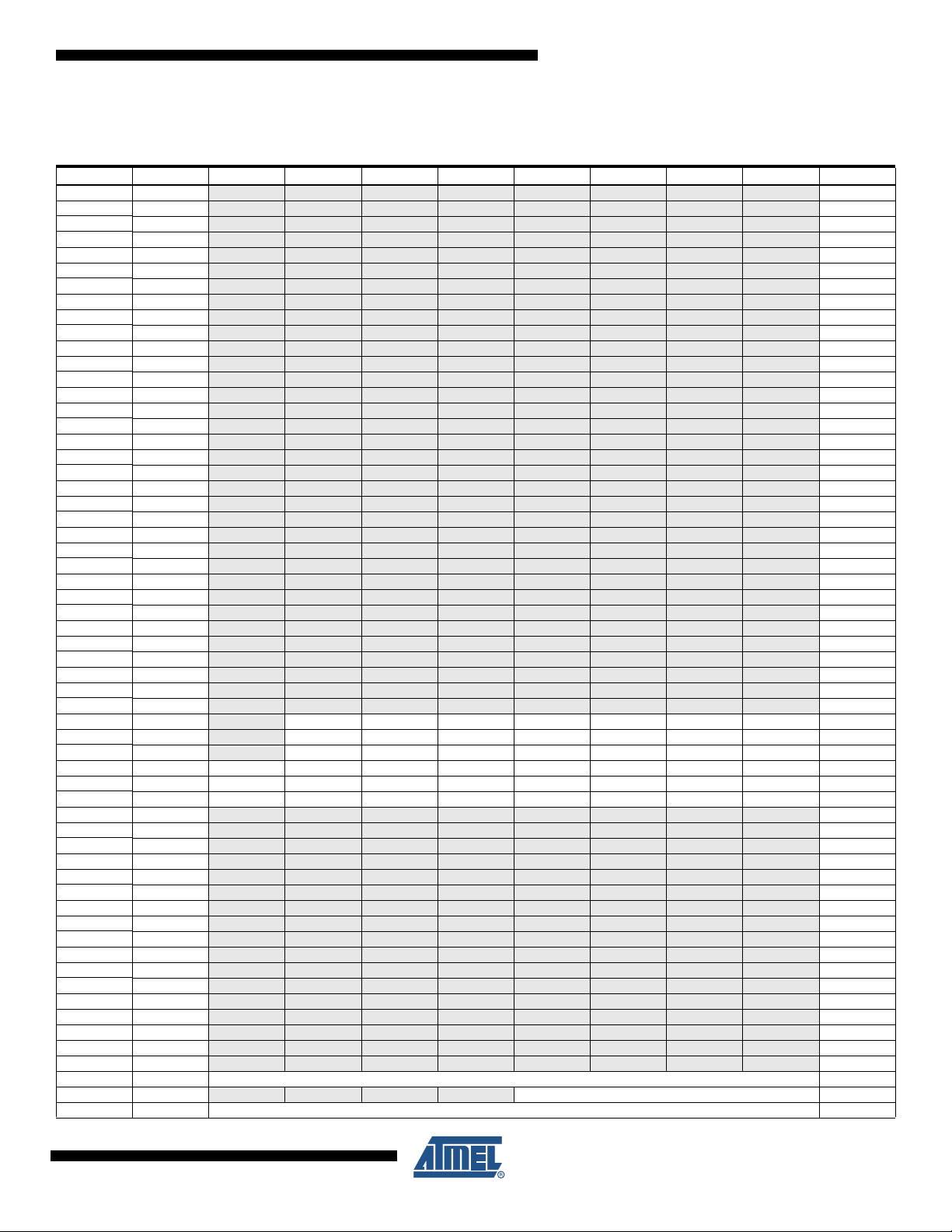
6. Register Summary
Note: Registers with bold type only available in ATmega3250/6450.
Address Name Bit 7 Bit 6 Bit 5 Bit 4 Bit 3 Bit 2 Bit 1 Bit 0 Page
(0xFF)
(0xFE)
(0xFD)
(0xFC)
(0xFB)
(0xFA)
(0xF9)
(0xF8)
(0xF7)
(0xF6)
(0xF5)
(0xF4)
(0xF3)
(0xF2)
(0xF1)
(0xF0)
(0xEF)
(0xEE)
(0xED)
(0xEC)
(0xEB)
(0xEA)
(0xE9)
(0xE8)
(0xE7)
(0xE6)
(0xE5)
(0xE4)
(0xE3)
(0xE2)
(0xE1)
(0xE0)
(0xDF)
(0xDE)
(0xDD)
(0xDC)
(0xDB)
(0xDA)
(0xD9)
(0xD8)
(0xD7)
(0xD6)
(0xD5)
(0xD4)
(0xD3)
(0xD2)
(0xD1)
(0xD0)
(0xCF)
(0xCE)
(0xCD)
(0xCC)
(0xCB)
(0xCA)
(0xC9)
(0xC8)
(0xC7)
(0xC6)
(0xC5)
(0xC4)
Reserved - - - - - - - Reserved - - - - - - - Reserved - - - - - - - Reserved - - - - - - - Reserved - - - - - - - Reserved - - - - - - - Reserved - - - - - - - Reserved - - - - - - - Reserved - - - - - - - Reserved - - - - - - - Reserved - - - - - - - Reserved - - - - - - - Reserved - - - - - - - Reserved - - - - - - - Reserved - - - - - - - Reserved - - - - - - - Reserved - - - - - - - Reserved - - - - - - - Reserved - - - - - - - Reserved - - - - - - - Reserved - - - - - - - Reserved - - - - - - - Reserved - - - - - - - Reserved - - - - - - - Reserved - - - - - - - Reserved - - - - - - - Reserved - - - - - - - Reserved - - - - - - - Reserved - - - - - - - Reserved - - - - - - - Reserved - - - - - - - Reserved - - - - - - - Reserved - - - - - - - Reserved - - - - - - - -
PORTJ - PORTJ6 PORTJ5 PORTJ4 PORTJ3 PORTJ2 PORTJ1 PORTJ0 83
DDRJ - DDJ6 DDJ5 DDJ4 DDJ3 DDJ2 DDJ1 DDJ0 83
PINJ - PINJ6 PINJ5 PINJ4 PINJ3 PINJ2 PINJ1 PINJ0 83
PORTH PORTH7 PORTH6 PORTH5 PORTH4 PORTH3 PORTH2 PORTH1 PORTH0 83
DDRH DDH7 DDH6 DDH5 DDH4 DDH3 DDH2 DDH1 DDH0 83
PINH PINH7 PINH6 PINH5 PINH4 PINH3 PINH2 PINH1 PINH0 83
Reserved
Reserved
Reserved
Reserved
Reserved
Reserved - - - - - - - Reserved
Reserved
Reserved - - - - - - - Reserved
Reserved
Reserved - - - - - - - Reserved
Reserved - - - - - - - Reserved
Reserved - - - - - - - Reserved
UDR0 USART0 Data Register 178
UBRR0H
UBRR0L USART0 Baud Rate Register Low 183
- - - - - - - -
- - - - - - - -
- - - - - - - -
- - - - - - - -
- - - - - - - -
- - - - - - - -
- - - - - - - -
- - - - - - - -
- - - - - - - -
- - - - - - - -
- - - - - - - -
- - - - - - - -
USART0 Baud Rate Register High 183
2570LS–AVR–08/07
9
Page 10

ATmega325/3250/645/6450
Address Name Bit 7 Bit 6 Bit 5 Bit 4 Bit 3 Bit 2 Bit 1 Bit 0 Page
(0xC3)
(0xC2)
(0xC1)
(0xC0)
(0xBF)
(0xBE)
(0xBD)
(0xBC)
(0xBB)
(0xBA)
(0xB9)
(0xB8)
(0xB7)
(0xB6)
(0xB5)
(0xB4)
(0xB3)
(0xB2)
(0xB1)
(0xB0)
(0xAF)
(0xAE)
(0xAD)
(0xAC)
(0xAB)
(0xAA)
(0xA9)
(0xA8)
(0xA7)
(0xA6)
(0xA5)
(0xA4)
(0xA3)
(0xA2)
(0xA1)
(0xA0)
(0x9F)
(0x9E)
(0x9D)
(0x9C)
(0x9B)
(0x9A)
(0x99)
(0x98)
(0x97)
(0x96)
(0x95)
(0x94)
(0x93)
(0x92)
(0x91)
(0x90)
(0x8F)
(0x8E)
(0x8D)
(0x8C)
(0x8B)
(0x8A)
(0x89)
(0x88)
(0x87)
(0x86)
(0x85)
Reserved - - - - - - - UCSR0C - UMSEL0 UPM01 UPM00 USBS0 UCSZ01 UCSZ00 UCPOL0 181
UCSR0B RXCIE0 TXCIE0 UDRIE0 RXEN0 TXEN0 UCSZ02 RXB80 TXB80 180
UCSR0A RXC0 TXC0 UDRE0 FE0 DOR0 UPE0 U2X0 MPCM0 179
Reserved - - - - - - - Reserved - - - - - - - Reserved
Reserved
Reserved - - - - - - - -
USIDR USI Data Register 191
USISR USISIF USIOIF USIPF USIDC USICNT3 USICNT2 USICNT1 USICNT0 192
USICR USISIE USIOIE USIWM1 USIWM0 USICS1 USICS0 USICLK USITC 193
Reserved - - - - - - - -
ASSR - - - EXCLK AS2 TCN2UB OCR2UB TCR2UB 144
Reserved - - - - - - - Reserved - - - - - - - -
OCR2A Timer/Counter 2 Output Compare Register A 144
TCNT2 Timer/Counter2 144
Reserved - - - - - - - -
TCCR2A FOC2A WGM20 COM2A1 COM2A0 WGM21 CS22 CS21 CS20 142
Reserved - - - - - - - Reserved - - - - - - - Reserved - - - - - - - Reserved - - - - - - - Reserved - - - - - - - Reserved - - - - - - - Reserved - - - - - - - Reserved - - - - - - - Reserved - - - - - - - Reserved - - - - - - - Reserved - - - - - - - Reserved - - - - - - - Reserved - - - - - - - Reserved - - - - - - - Reserved - - - - - - - Reserved - - - - - - - Reserved - - - - - - - Reserved - - - - - - - Reserved - - - - - - - Reserved - - - - - - - Reserved - - - - - - - Reserved
Reserved - - - - - - - Reserved
Reserved
Reserved
Reserved
Reserved - - - - - - - Reserved
Reserved
Reserved - - - - - - - Reserved
Reserved
Reserved - - - - - - - Reserved
Reserved - - - - - - - OCR1BH Timer/Counter1 Output Compare Register B High 126
OCR1BL Timer/Counter1 Output Compare Register B Low 126
OCR1AH Timer/Counter1 Output Compare Register A High 126
OCR1AL Timer/Counter1 Output Compare Register A Low 126
ICR1H Timer/Counter1 Input Capture Register High 126
ICR1L Timer/Counter1 Input Capture Register Low 126
TCNT1H Timer/Counter1 High 126
- - - - - - - -
- - - - - - - -
- - - - - - - -
- - - - - - - -
- - - - - - - -
- - - - - - - -
- - - - - - - -
- - - - - - - -
- - - - - - - -
- - - - - - - -
- - - - - - - -
- - - - - - - -
10
2570LS–AVR–08/07
Page 11

ATmega325/3250/645/6450
Address Name Bit 7 Bit 6 Bit 5 Bit 4 Bit 3 Bit 2 Bit 1 Bit 0 Page
(0x84)
(0x83)
(0x82)
(0x81)
(0x80)
(0x7F)
(0x7E)
(0x7D)
(0x7C)
(0x7B)
(0x7A)
(0x79)
(0x78)
(0x77)
(0x76)
(0x75)
(0x74)
(0x73)
(0x72)
(0x71)
(0x70)
(0x6F)
(0x6E)
(0x6D)
(0x6C)
(0x6B)
(0x6A)
(0x69)
(0x68)
(0x67)
(0x66)
(0x65)
(0x64)
(0x63)
(0x62)
(0x61)
(0x60)
0x3F (0x5F)
0x3E (0x5E)
0x3D (0x5D)
0x3C (0x5C)
0x3B (0x5B)
0x3A (0x5A)
0x39 (0x59)
0x38 (0x58)
0x37 (0x57)
0x36 (0x56)
0x35 (0x55)
0x34 (0x54)
0x33 (0x53)
0x32 (0x52)
0x31 (0x51)
0x30 (0x50)
0x2F (0x4F)
0x2E (0x4E)
0x2D (0x4D)
0x2C (0x4C)
0x2B (0x4B)
0x2A (0x4A)
0x29 (0x49)
0x28 (0x48)
0x27 (0x47)
0x26 (0x46)
TCNT1L Timer/Counter1 Low 126
Reserved - - - - - - - -
TCCR1C FOC1A FOC1B - - - - - -125
TCCR1B ICNC1 ICES1 - WGM13WGM12CS12CS11CS10 124
TCCR1A COM1A1 COM1A0 COM1B1 COM1B0 - -WGM11WGM10122
DIDR1 - - - - - - AIN1D AIN0D 199
DIDR0 ADC7D ADC6D ADC5D ADC4D ADC3D ADC2D ADC1D ADC0D 216
Reserved - - - - - - - -
ADMUX REFS1 REFS0 ADLAR MUX4 MUX3 MUX2 MUX1 MUX0 212
ADCSRB -ACME- - - ADTS2 ADTS1 ADTS0 197/216
ADCSRA ADEN ADSC ADATE ADIF ADIE ADPS2 ADPS1 ADPS0 214
ADCH ADC Data Register High 215
ADCL ADC Data Register Low 215
Reserved - - - - - - - Reserved - - - - - - - Reserved - - - - - - - Reserved - - - - - - - PCMSK3 - PCINT30 PCINT29 PCINT28 PCINT27 PCINT26 PCINT25 PCINT24 57
Reserved - - - - - - - Reserved - - - - - - - -
TIMSK2 - - - - - - OCIE2A TOIE2 145
TIMSK1 - -ICIE1- - OCIE1B OCIE1A TOIE1 127
TIMSK0 - - - - - - OCIE0A TOIE0 98
PCMSK2 PCINT23 PCINT22 PCINT21 PCINT20 PCINT19 PCINT18 PCINT17 PCINT16 57
PCMSK1 PCINT15 PCINT14 PCINT13 PCINT12 PCINT11 PCINT10 PCINT9 PCINT8 58
PCMSK0 PCINT7 PCINT6 PCINT5 PCINT4 PCINT3 PCINT2 PCINT1 PCINT0 58
Reserved - - - - - - - -
EICRA - - - - - -ISC01ISC0055
Reserved - - - - - - - Reserved - - - - - - - OSCCAL Oscillator Calibration Register [CAL7..0] 31
Reserved - - - - - - - -
PRR - - - - PRTIM1 PRSPI PSUSART0 PRADC 39
Reserved - - - - - - - Reserved - - - - - - - -
CLKPR CLKPCE - - - CLKPS3 CLKPS2 CLKPS1 CLKPS0 31
WDTCR - - - WDCE WDE WDP2 WDP1 WDP0 46
SREG I T H S V N Z C 11
SPH Stack Pointer High 13
SPL Stac k Pointer Low 13
Reserved - - - - - - - Reserved
Reserved - - - - - - - Reserved
Reserved
SPMCSR SPMIE RWWSB
Reserved
MCUCR JTD - -PUD- - IVSEL IVCE 52/80/226
MCUSR
SMCR
Reserved - - - - - - - -
OCDR IDRD/OCDR7 OCDR6 OCDR5 OCDR4 OCDR3 OCDR2 OCDR1 OCDR0 222
ACSR ACD ACBG ACO ACI ACIE ACIC ACIS1 ACIS0 197
Reserved - - - - - - - -
SPDR SPI Data Register 155
SPSR SPIF WCOL
SPCR SPIE SPE DORD MSTR CPOL CPHA SPR1 SPR0 153
GPIOR2 General Purpose I/O Register 24
GPIOR1 General Purpose I/O Register 24
Reserved
Reserved - - - - - - - -
OCR0A Timer/Counter0 Output Compare A 97
TCNT0 Timer/Counter0 97
- - - - - - - -
- - - - - - - -
- - - - - - - -
- RWWSRE BLBSET PGWRT PGERS SPMEN 262
- - - JTRF WDRF BORF EXTRF PORF 46
- - - - SM2 SM1 SM0 SE 34
- - - - - SPI2X 155
- - - - - - - -
2570LS–AVR–08/07
11
Page 12

ATmega325/3250/645/6450
Address Name Bit 7 Bit 6 Bit 5 Bit 4 Bit 3 Bit 2 Bit 1 Bit 0 Page
0x25 (0x45)
0x24 (0x44)
0x23 (0x43)
0x22 (0x42)
0x21 (0x41)
0x20 (0x40)
0x1F (0x3F)
0x1E (0x3E)
0x1D (0x3D)
0x1C (0x3C)
0x1B (0x3B)
0x1A (0x3A)
0x19 (0x39)
0x18 (0x38)
0x17 (0x37)
0x16 (0x36)
0x15 (0x35)
0x14 (0x34)
0x13 (0x33)
0x12 (0x32)
0x11 (0x31)
0x10 (0x30)
0x0F (0x2F)
0x0E (0x2E)
0x0D (0x2D)
0x0C (0x2C)
0x0B (0x2B)
0x0A (0x2A)
0x09 (0x29)
0x08 (0x28)
0x07 (0x27)
0x06 (0x26)
0x05 (0x25)
0x04 (0x24)
0x03 (0x23)
0x02 (0x22)
0x01 (0x21)
0x00 (0x20)
Reserved - - - - - - - -
TCCR0A FOC0A WGM00 COM0A1 COM0A0 WGM01 CS02 CS01 CS00 95
GTCCR TSM - - - - - PSR2 PSR10 100/146
EEARH - - - - - EEPROM Address Register High 21
EEARL EEPROM Address Register Low 21
EEDR EEPROM Data Register 21
EECR
GPIOR0 General Purpose I/O Register 24
EIMSK PCIE3 PCIE2 PCIE1 PCIE0
EIFR PCIF3 PCIF2 PCIF1 PCIF0 - - - INTF0 56
Reserved - - - - - - - Reserved - - - - - - - Reserved - - - - - - - Reserved - - - - - - - -
TIFR2 - - - - - -OCF2ATOV2146
TIFR1 - -ICF1- -OCF1BOCF1ATOV1127
TIFR0 - - - - - -OCF0ATOV098
PORTG - - - PORTG4 PORTG3 PORTG2 PORTG1 PORTG0 82
DDRG - - - DDG4 DDG3 DDG2 DDG1 DDG0 83
PING - - PING5 PING4 PING3 PING2 PING1 PING0 83
PORTF PORTF7 PORTF6 PORTF5 PORTF4 PORTF3 PORTF2 PORTF1 PORTF0 82
DDRF DDF7 DDF6 DDF5 DDF4 DDF3 DDF2 DDF1 DDF0 82
PINF PINF7 PINF6 PINF5 PINF4 PINF3 PINF2 PINF1 PINF0 82
PORTE PORTE7 PORTE6 PORTE5 PORTE4 PORTE3 PORTE2 PORTE1 PORTE0 82
DDRE DDE7 DDE6 DDE5 DDE4 DDE3 DDE2 DDE1 DDE0 82
PINE PINE7 PINE6 PINE5 PINE4 PINE3 PINE2 PINE1 PINE0 82
PORTD PORTD7 PORTD6 PORTD5 PORTD4 PORTD3 PORTD2 PORTD1 PORTD0 81
DDRD DDD7 DDD6 DDD5 DDD4 DDD3 DDD2 DDD1 DDD0 81
PIND PIND7 PIND6 PIND5 PIND4 PIND3 PIND2 PIND1 PIND0 82
PORTC PORTC7 PORTC6 PORTC5 PORTC4 PORTC3 PORTC2 PORTC1 PORTC0 81
DDRC DDC7 DDC6 DDC5 DDC4 DDC3 DDC2 DDC1 DDC0 81
PINC PINC7 PINC6 PINC5 PINC4 PINC3 PINC2 PINC1 PINC0 81
PORTB PORTB7 PORTB6 PORTB5 PORTB4 PORTB3 PORTB2 PORTB1 PORTB0 81
DDRB DDB7 DDB6 DDB5 DDB4 DDB3 DDB2 DDB1 DDB0 81
PINB PINB7 PINB6 PINB5 PINB4 PINB3 PINB2 PINB1 PINB0 81
PORTA P ORTA7 PO RTA 6 PO RTA5 PO RTA4 PO RTA3 P ORTA2 PO RTA 1 PORTA 0 80
DDRA DDA7 DDA6 DDA5 DDA4 DDA3 DDA2 DDA1 DDA0 80
PINA PINA7 PINA6 PINA5 PINA4 PINA3 PINA2 PINA1 PINA0 80
- - - - EERIE EEMWE EEWE EERE 21
- - -INT056
Note: 1. For compatibility with future devices, reserved bits should be written to zero if accessed. Reserved I/O memory addresses
should never be written.
2. I/O Registers within the address range 0x00 - 0x1F are directly bit-accessible using the SBI and CBI instructions. In these
registers, the value of single bits can be checked by using the SBIS and SBIC instructions.
3. Some of the Status Flags are cleared by writing a logical one to them. Note that, unlike most other AVRs, the CBI and SBI
instructions will only operate on the specified bit, and can therefore be used on registers containing such Status Flags. The
CBI and SBI instructions work with registers 0x00 to 0x1F only.
4. When using the I/O specific commands IN and OUT, the I/O addresses 0x00 - 0x3F must be used. When addressing I/O
Registers as data space using LD and ST instructions, 0x20 must be added to these addresses. The
ATmega325/3250/645/6450 is a complex microcontroller with more peripheral units than can be supported within the 64
location reserved in Opcode for the IN and OUT instructions. For the Extended I/O space from 0x60 - 0xFF in SRAM, only
the ST/STS/STD and LD/LDS/LDD instructions can be used.
12
2570LS–AVR–08/07
Page 13
ATmega325/3250/645/6450
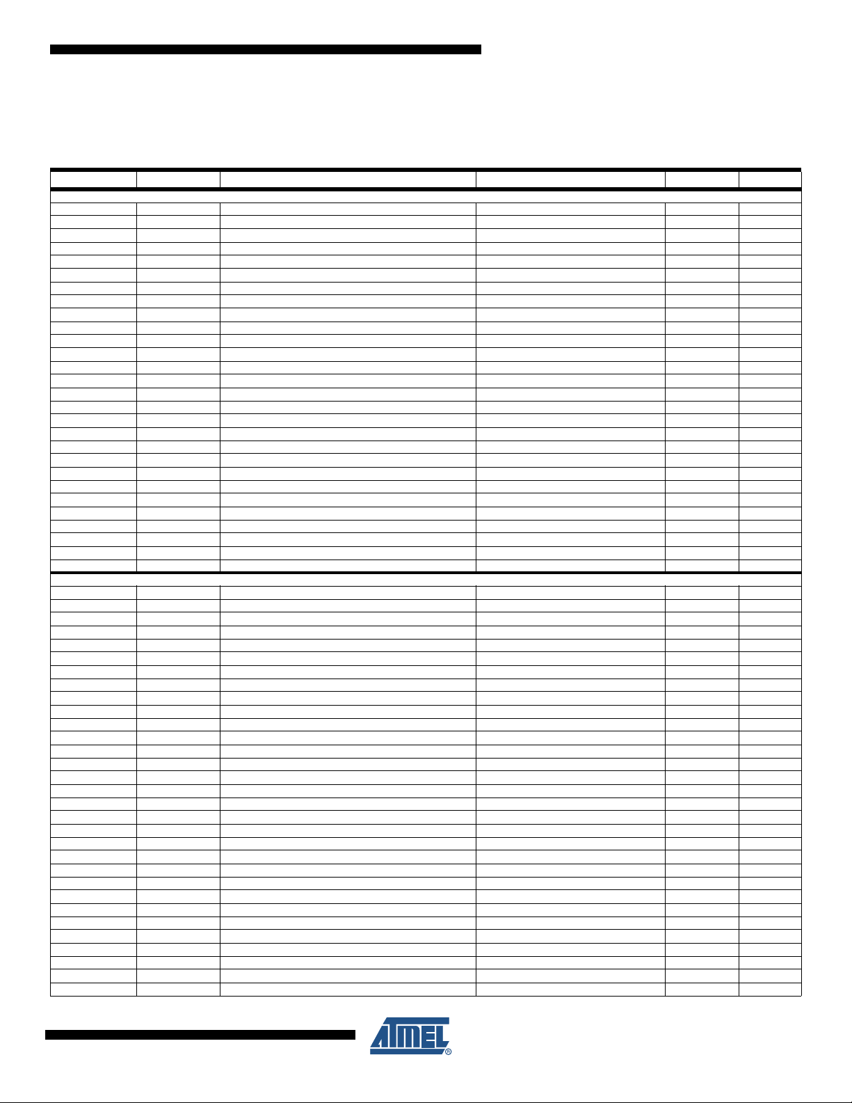
7. Instruction Set Summary
Mnemonics Operands Description Operation Flags #Clocks
ARITHMETIC AND LOGIC INSTRUCTIONS
ADD Rd, Rr Add two Registers Rd ← Rd + Rr Z,C,N,V,H 1
ADC Rd, Rr Add with Carry two Registers Rd ← Rd + Rr + C Z,C,N,V,H 1
ADIW Rdl,K Add Immediate to Word Rdh:Rdl ← Rdh:Rdl + K Z,C,N,V,S 2
SUB Rd, Rr Subtract two Registers Rd ← Rd - Rr Z,C,N,V,H 1
SUBI Rd, K Subtract Constant from Register Rd ← Rd - K Z,C,N,V,H 1
SBC Rd, Rr Subtract with Carry two Registers Rd ← Rd - Rr - C Z,C,N,V,H 1
SBCI Rd, K Subtract with Carry Constant from Reg. Rd ← Rd - K - C Z,C,N,V,H 1
SBIW Rdl,K Subtract Immediate from Word Rdh:Rdl ← Rdh:Rdl - K Z,C,N,V,S 2
AND Rd, Rr Logical AND Registers Rd ← Rd • Rr Z,N,V 1
ANDI Rd, K Logical AND Register and Constant Rd ← Rd • K Z,N,V 1
OR Rd, Rr Logical OR Registers Rd ← Rd v Rr Z,N,V 1
ORI Rd, K Logical OR Register and Constant Rd ← Rd v K Z,N,V 1
EOR Rd, Rr Exclusive OR Registers Rd ← Rd ⊕ Rr Z,N,V 1
COM Rd One’s Complement Rd ← 0xFF − Rd Z,C,N,V 1
NEG Rd Two’s Complement Rd ← 0x00 − Rd Z,C,N,V,H 1
SBR Rd,K Set Bit(s) in Register Rd ← Rd v K Z,N,V 1
CBR Rd,K Clear Bit(s) in Register Rd ← Rd • (0xFF - K) Z,N,V 1
INC Rd Increment Rd ← Rd + 1 Z,N,V 1
DEC Rd Decrement Rd ← Rd − 1 Z,N,V 1
TST Rd Test for Zero or Minus Rd ← Rd • Rd Z,N,V 1
CLR Rd Clear Register Rd ← Rd ⊕ Rd Z,N,V 1
SER Rd Set Register Rd ← 0xFF None 1
MUL Rd, Rr Multiply Unsigned R1:R0 ← Rd x Rr Z,C 2
MULS Rd, Rr Multiply Signed R1:R0 ← Rd x Rr Z,C 2
MULSU Rd, Rr Multiply Signed with Unsigned R1:R0 ← Rd x Rr Z,C 2
FMUL Rd, Rr Fractional Multiply Unsigned R1:R0 ← (Rd x Rr) << 1 Z,C 2
FMULS Rd, Rr Fractional Multiply Signed R1:R0 ← (Rd x Rr) << 1 Z,C 2
FMULSU Rd, Rr Fractional Multiply Signed with Unsigned R1:R0 ← (Rd x Rr) << 1 Z,C 2
BRANCH INSTRUCTIONS
RJMP k Relative Jump PC ← PC + k + 1 None 2
IJMP Indirect Jump to (Z) PC ← Z None 2
JMP k Direct Jump PC ← kNone3
RCALL k Relative Subroutine Call PC ← PC + k + 1 None 3
ICALL Indirect Call to (Z) PC ← ZNone3
CALL k Direct Subroutine Call PC ← kNone4
RET Subroutine Return PC ← STACK None 4
RETI Interrupt Return PC ← STACK I 4
CPSE Rd,Rr Compare, Skip if Equal if (Rd = Rr) PC ← PC + 2 or 3 None 1/2/3
CP Rd,Rr Compare Rd − Rr Z, N,V,C,H 1
CPC Rd,Rr Compare with Carry Rd − Rr − C Z, N,V,C,H 1
CPI Rd,K Compare Register with Immediate Rd − K Z, N,V,C,H 1
SBRC Rr, b Skip if Bit in Register Cleared if (Rr( b)=0) PC ← PC + 2 or 3 None 1/2/3
SBRS Rr, b Skip if Bit in Register is Set if (Rr(b)=1) PC ← PC + 2 or 3 None 1/2/3
SBIC P, b Skip if Bit in I/O Register Cleared if (P(b)=0) PC ← PC + 2 or 3 None 1/2/3
SBIS P, b Skip if Bit in I/O Register is Set if (P(b)=1) PC ← PC + 2 or 3 None 1/2/3
BRBS s, k Branch if Status Flag Set if (SREG(s) = 1) then PC←PC+k + 1 None 1/2
BRBC s, k Branch if Status Flag Cleared if (S REG(s) = 0) then PC←PC+k + 1 None 1/2
BREQ k Branch if Equal if (Z = 1) then PC ← PC + k + 1 None 1/2
BRNE k Branch if Not Equal if (Z = 0) then PC ← PC + k + 1 None 1/2
BRCS k Branch if Carry Set if (C = 1) then PC ← PC + k + 1 None 1/2
BRCC k Branch if Carry Cleared if (C = 0) then PC ← PC + k + 1 None 1/2
BRSH k Branch if Same or Higher if (C = 0) then PC ← PC + k + 1 None 1/2
BRLO k Branch if Lower if (C = 1) then PC ← PC + k + 1 None 1/2
BRMI k Branch if Minus if (N = 1) then PC ← PC + k + 1 None 1/2
BRPL k Branch if Plus if (N = 0) then PC ← PC + k + 1 None 1/2
BRGE k Branch if Greater or Equal, Signed if (N ⊕ V= 0) then PC ← PC + k + 1 None 1/2
BRLT k Branch if Less Than Zero, Signed if (N ⊕ V= 1) then PC ← PC + k + 1 None 1/2
BRHS k Branch if Half Carry Flag Set if (H = 1) then PC ← PC + k + 1 None 1/2
BRHC k Branch if Half Carry Flag Cle ared if (H = 0) then PC ← PC + k + 1 None 1/2
BRTS k Branch if T Flag Set if (T = 1) then PC ← PC + k + 1 None 1/2
2570LS–AVR–08/07
13
Page 14

ATmega325/3250/645/6450
Mnemonics Operands Description Operation Flags #Clocks
BRTC k Branch if T Flag Cleared if (T = 0) then PC ← PC + k + 1 None 1/2
BRVS k Branch if Overflow Flag is Set if (V = 1) then PC ← PC + k + 1 None 1/2
BRVC k Branch if Overflow Flag is Cleared if (V = 0) then PC ← PC + k + 1 None 1/2
BRIE k Branch if Interrupt Enabled if ( I = 1) then PC ← PC + k + 1 None 1/2
BRID k Branch if Interrupt Disabled if ( I = 0) then PC ← PC + k + 1 None 1/2
BIT AND BIT-TEST INSTRUCTIONS
SBI P,b Set Bit in I/O Register I/O(P,b) ← 1None2
CBI P,b Clear Bit in I/O Register I/O(P,b) ← 0None2
LSL Rd Logical Shift Left Rd(n+1) ← Rd(n), Rd(0) ← 0 Z,C,N,V 1
LSR Rd Logical Shift Right Rd(n) ← Rd(n+1), Rd(7) ← 0 Z,C,N,V 1
ROL Rd Rotate Left Through Carry Rd(0)←C,Rd(n+1)← Rd(n),C←Rd(7) Z,C,N,V 1
ROR Rd Rotate Right Through Carry Rd(7)←C,Rd(n)← Rd(n+1),C←Rd(0) Z,C,N,V 1
ASR Rd Arithmetic Shift Right Rd(n) ← Rd(n+1), n=0..6 Z,C,N,V 1
SWAP Rd Swap Nibbles Rd(3..0)←Rd(7..4),Rd(7..4)←Rd(3..0) None 1
BSET s Flag Set SREG(s) ← 1 SREG(s) 1
BCLR s Flag Clear SR EG(s) ← 0 SREG(s) 1
BST Rr, b Bit Store from Register to T T ← Rr(b) T 1
BLD Rd, b Bit load from T to Register Rd(b) ← TNone1
SEC Set Carry C ← 1C1
CLC Clear Carry C ← 0 C 1
SEN Set Negative Flag N ← 1N1
CLN Clear Negative Flag N ← 0 N 1
SEZ Set Zero Flag Z ← 1Z1
CLZ Clear Zero Flag Z ← 0 Z 1
SEI Global Interrupt Enable I ← 1I1
CLI Global Interrupt Disable I ← 0 I 1
SES Set Signed Test Flag S ← 1S1
CLS Clear Signed Test Flag S ← 0 S 1
SEV Set Twos Complement Overflow. V ← 1V1
CLV Clear Twos Complement Overflow V ← 0 V 1
SET Set T in SREG T ← 1T1
CLT Clear T in SREG T ← 0 T 1
SEH Set Half Carry Flag in SREG H ← 1H1
CLH Clear Half Carry Flag in SREG H ← 0 H 1
DATA TRANSFER INSTRUCTIONS
MOV Rd, Rr Move Between Registers Rd ← Rr None 1
MOVW Rd, Rr Copy Register Word
LDI Rd, K Load Immediate Rd ← KNone1
LD Rd, X Load Indirect Rd ← (X) None 2
LD Rd, X+ Load Indirect and Post-Inc. Rd ← (X), X ← X + 1 None 2
LD Rd, - X Load Indirect and Pre-Dec. X ← X - 1, Rd ← (X) None 2
LD Rd, Y Load Indirect Rd ← (Y) None 2
LD Rd, Y+ Load Indirect and Post-Inc. Rd ← (Y), Y ← Y + 1 None 2
LD Rd, - Y Load Indirect and Pre-Dec. Y ← Y - 1, Rd ← (Y) None 2
LDD Rd,Y+q Load Indirect with Displacement Rd ← (Y + q) None 2
LD Rd, Z Load Indirect Rd ← (Z) None 2
LD Rd, Z+ Load Indirect and Post-Inc. Rd ← (Z), Z ← Z+1 None 2
LD Rd, -Z Load Indirect and Pre-Dec. Z ← Z - 1, Rd ← (Z) None 2
LDD Rd, Z+q Load Indirect with Displacement Rd ← (Z + q) None 2
LDS Rd, k Load Direct from SRAM Rd ← (k) None 2
ST X, Rr Store Indirect (X) ← Rr None 2
ST X+, Rr Store Indirect and Post-Inc. (X) ← Rr, X ← X + 1 None 2
ST - X, Rr Store Indirect and Pre-Dec. X ← X - 1, (X) ← Rr None 2
ST Y, Rr Store Indirect (Y) ← Rr None 2
ST Y+, Rr Store Indirect and Post-Inc. (Y) ← Rr, Y ← Y + 1 None 2
ST - Y, Rr Store Indirect and Pre-Dec. Y ← Y - 1, (Y) ← Rr None 2
STD Y+q,Rr Store Indirect with Displacement (Y + q) ← Rr None 2
ST Z, Rr Store Indirect (Z) ← Rr None 2
ST Z+, Rr Store Indirect and Post-Inc. (Z) ← Rr, Z ← Z + 1 None 2
ST -Z, Rr Store Indirect and Pre-Dec. Z ← Z - 1, (Z) ← Rr None 2
STD Z+q,Rr Store Indirect with Displ ace ment (Z + q) ← Rr None 2
STS k, Rr Store Direct to SRAM (k) ← Rr None 2
LPM Load Program Memory R0 ← (Z) None 3
LPM Rd, Z Load Program Memory Rd ← (Z) N one 3
LPM Rd, Z+ Load Program Memory and Post-Inc Rd ← (Z), Z ← Z+1 None 3
SPM Store Program Memory (Z) ← R1:R0 None -
Rd+1:Rd ← Rr+1:Rr
None 1
14
2570LS–AVR–08/07
Page 15

ATmega325/3250/645/6450
Mnemonics Operands Description Operation Flags #Clocks
IN Rd, P In Port Rd ← PNone1
OUT P, Rr Out Port P ← Rr None 1
PUSH Rr Push Register on Stack STACK ← Rr None 2
POP Rd Pop Register from Stack Rd ← STACK None 2
MCU CONTROL INSTRUCTIONS
NOP No Operation None 1
SLEEP Sleep (see specific descr. for Sleep function) None 1
WDR Watchdog Reset (see specific descr. for WDR/timer) None 1
BREAK Break For On-chip Debug Only None N/A
2570LS–AVR–08/07
15
Page 16

ATmega325/3250/645/6450
8. Ordering Information
8.1 ATmega325
Speed (MHz)
Notes: 1. This device can also be supplied in wafer form. Please contact your local Atmel sales office for detailed ordering information
2. Pb-free packaging alternative, complies to the European Directive for Restriction of Hazardous Substances (RoHS direc-
3. For Speed Grades see Figure 28-1 on page 298 and Figure 28-2 on page 298.
(3)
8 1.8 - 5.5V
16 2.7 - 5.5V
and minimum quantities.
tive). Also Halide free and fully Green.
Power Supply Ordering Code Package Type
ATmega325V -8AI
ATmega325V-8AU
ATmega325V -8MI
ATmega325V -8MU
ATmega325-16AI
ATmega325-16AU
ATmega325-16MI
ATmega325-16MU
(2)
(2)
(2)
(2)
64A
64A
64M1
64M1
64A
64A
64M1
64M1
(1)
Operational Range
Industrial
0°C to 85°C)
(-4
Industrial
0°C to 85°C)
(-4
16
2570LS–AVR–08/07
Page 17

ATmega325/3250/645/6450
Package Type
64A 64-lead , 14 x 14 x 1.0 mm, Thin Profile Plastic Quad Flat Package (TQFP)
64M1 64-pad, 9 x 9 x 1.0 mm, Quad Flat No-Lead/Micro Lead Frame Package (QFN/MLF)
100A 100-lead, 14 x 14 x 1.0 mm, 0.5 mm Lead Pitch, Thin Profile Plastic Quad Flat Package (TQFP)
2570LS–AVR–08/07
17
Page 18

ATmega325/3250/645/6450
8.2 ATmega3250
Speed (MHz)
Notes: 1. This device can also be supplied in wafer form. Please contact your local Atmel sales office for detailed ordering information
2. Pb-free packaging alternative, complies to the European Directive for Restriction of Hazardous Substances (RoHS direc-
3. For Speed Grades see Figure 28-1 on page 298 and Figure 28-2 on page 298.
(3)
8 1.8 - 5.5V
16 2.7 - 5.5V
and minimum quantities.
tive). Also Halide free and fully Green.
Power Supply Ordering Code Package Type
ATmega3250V -8AI
ATmega3250V-8AU
ATmega3250-16AI
ATmega3250-16AU
(2)
(2)
100A
100A
100A
100A
(1)
Operational Range
Industrial
0°C to 85°C)
(-4
Industrial
(-4
0°C to 85°C)
64A 64-lead , 14 x 14 x 1.0 mm, Thin Profile Plastic Quad Flat Package (TQFP)
64M1 64-pad, 9 x 9 x 1.0 mm, Quad Flat No-Lead/Micro Lead Frame Package (QFN/MLF)
100A 100-lead, 14 x 14 x 1.0 mm, 0.5 mm Lead Pitch, Thin Profile Plastic Quad Flat Package (TQFP)
18
Package Type
2570LS–AVR–08/07
Page 19

ATmega325/3250/645/6450
8.3 ATmega645
Speed (MHz)
(3)
Power Supply Ordering Code Package Type
8 1.8 - 5.5V
16 2.7 - 5.5V
ATmega645V -8AI
ATmega645V-8AU
ATmega645V -8MI
ATmega645V -8MU
ATmega645-16AI
ATmega645-16AU
ATmega645-16MI
ATmega645-16MU
(2)
(2)
(2)
(2)
64A
64A
64M1
64M1
64A
64A
64M1
64M1
Notes: 1. This device can also be supplied in wafer form. Please contact your local Atmel sales office for detailed ordering information
and minimum quantities.
2. Pb-free packaging alternative, complies to the European Directive for Restriction of Hazardous Substances (RoHS directive). Also Halide free and fully Green.
3. For Speed Grades see Figure 28-1 on page 298 and Figure 28-2 on page 298.
(1)
Operational Range
Industrial
0°C to 85°C)
(-4
Industrial
(-40°C to 85°C)
Package Type
64A 64-lead , 14 x 14 x 1.0 mm, Thin Profile Plastic Quad Flat Package (TQFP)
64M1 64-pad, 9 x 9 x 1.0 mm, Quad Flat No-Lead/Micro Lead Frame Package (QFN/MLF)
100A 100-lead, 14 x 14 x 1.0 mm, 0.5 mm Lead Pitch, Thin Profile Plastic Quad Flat Package (TQFP)
2570LS–AVR–08/07
19
Page 20

ATmega325/3250/645/6450
8.4 ATmega6450
Speed (MHz)
Notes: 1. This device can also be supplied in wafer form. Please contact your local Atmel sales office for detailed ordering information
2. Pb-free packaging alternative, complies to the European Directive for Restriction of Hazardous Substances (RoHS direc-
3. For Speed Grades see Figure 28-1 on page 298 and Figure 28-2 on page 298.
(3)
8 1.8 - 5.5V
16 2.7 - 5.5V
and minimum quantities.
tive). Also Halide free and fully Green.
Power Supply Ordering Code Package Type
ATmega6450V -8AI
ATmega6450V-8AU
ATmega6450-16AI
ATmega6450-16AU
(2)
(2)
100A
100A
100A
100A
(1)
Operational Range
Industrial
0°C to 85°C)
(-4
Industrial
(-4
0°C to 85°C)
64A 64-lead , 14 x 14 x 1.0 mm, Thin Profile Plastic Quad Flat Package (TQFP)
64M1 64-pad, 9 x 9 x 1.0 mm, Quad Flat No-Lead/Micro Lead Frame Package (QFN/MLF)
100A 100-lead, 14 x 14 x 1.0 mm, 0.5 mm Lead Pitch, Thin Profile Plastic Quad Flat Package (TQFP)
20
Package Type
2570LS–AVR–08/07
Page 21

9. Packaging Information
9.1 64A
PIN 1
PIN 1 IDENTIFIER
ATmega325/3250/645/6450
B
e
E1 E
D1
D
C
0°~7°
A1
L
Notes:
1.This package conforms to JEDEC reference MS-026, Variation AEB.
2. Dimensions D1 and E1 do not include mold protrusion. Allowable
protrusion is 0.25 mm per side. Dimensions D1 and E1 are maximum
plastic body size dimensions including mold mismatch.
3. Lead coplanarity is 0.10 mm maximum.
A2 A
SYMBOL
COMMON DIMENSIONS
(Unit of Measure = mm)
MIN
A – – 1.20
A1 0.05 – 0.15
A2 0.95 1.00 1.05
D 15.75 16.00 16.25
D1 13.90 14.00 14.10 Note 2
E 15.75 16.00 16.25
E1 13.90 14.00 14.10 Note 2
B 0.30 – 0.45
C 0.09 – 0.20
L 0.45 – 0.75
e 0.80 TYP
NOM
MAX
NOTE
2570LS–AVR–08/07
2325 Orchard Parkway
R
San Jose, CA 95131
TITLE
64A, 64-lead, 14 x 14 mm Body Size, 1.0 mm Body Thickness,
0.8 mm Lead Pitch, Thin Profile Plastic Quad Flat Package (TQFP)
10/5/2001
DRAWING NO.
64A
REV.
B
21
Page 22

ATmega325/3250/645/6450
9.2 64M1
D
Marked Pin# 1 ID
E
SEATING PLANE
C
TOP VIEW
A1
A
K
L
D2
E2
K
b
e
BOTTOM VIEW
1. JEDEC Standard MO-220, (SAW Singulation) Fig. 1, VMMD.
Note:
2. Dimension and tolerance conform to ASMEY14.5M-1994.
Pin #1 Corner
1
2
3
Option A
Option B
Option C
Pin #1
Triangle
Pin #1
Chamfer
(C 0.30)
Pin #1
Notch
(0.20 R)
SIDE VIEW
SYMBOL
A 0.80 0.90 1.00
A1 – 0.02 0.05
b 0.18 0.25 0.30
D
D2 5.20 5.40 5.60
E
E2 5.20 5.40 5.60
e 0.50 BSC
L 0.35 0.40 0.45
K 1.25 1.40 1.55
0.08
C
COMMON DIMENSIONS
(Unit of Measure = mm)
MIN
8.90 9.00 9.10
8.90 9.00 9.10
NOM
MAX
NOTE
2325 Orchard Parkway
R
San Jose, CA 95131
TITLE
64M1, 64-pad, 9 x 9 x 1.0 mm Body, Lead Pitch 0.50 mm,
5.40 mm Exposed Pad, Micro Lead Frame Package (MLF)
22
5/25/06
DRAWING NO.
64M1
REV.
G
2570LS–AVR–08/07
Page 23

9.3 100A
ATmega325/3250/645/6450
PIN 1
B
PIN 1 IDENTIFIER
e
E1 E
D1
D
C
0˚~7˚
A1
L
Notes: 1. This package conforms to JEDEC reference MS-026, Variation AED.
2. Dimensions D1 and E1 do not include mold protrusion. Allowable
protrusion is 0.25 mm per side. Dimensions D1 and E1 are maximum
plastic body size dimensions including mold mismatch.
3. Lead coplanarity is 0.08 mm maximum.
A2 A
SYMBOL
COMMON DIMENSIONS
(Unit of Measure = mm)
MIN
A – – 1.20
A1 0.05 – 0.15
A2 0.95 1.00 1.05
D 15.75 16.00 16.25
D1 13.90 14.00 14.10 Note 2
E 15.75 16.00 16.25
E1 13.90 14.00 14.10 Note 2
B 0.17 – 0.27
C 0.09 – 0.20
L 0.45 – 0.75
e 0.50 TYP
NOM
MAX
NOTE
2570LS–AVR–08/07
2325 Orchard Parkway
R
San Jose, CA 95131
TITLE
100A, 100-lead, 14 x 14 mm Body Size, 1.0 mm Body Thickness,
0.5 mm Lead Pitch, Thin Profile Plastic Quad Flat Package (TQFP)
10/5/2001
DRAWING NO.
100A
REV.
C
23
Page 24

ATmega325/3250/645/6450
10. Errata
10.1 Errata ATmega325
The revision letter in this section refers to the revision of the ATmega325 device.
10.1.1 ATmega325 Rev. C
•
Interrupts may be lost when writing the timer registers in the asynchronous timer
1. Interrupts may be lost when writing the timer registers in the asynchronous timer
10.1.2 ATmega325 Rev. B
Not sampled.
10.1.3 ATmega325 Rev. A
•
Interrupts may be lost when writing the timer registers in the asynchronous timer
1. Interrupts may be lost when writing the timer registers in the asynchronous timer
If one of the timer registers which is synchronized to the asynchronous timer2 clock is written in the cycle before a overflow interrupt occurs, the interrupt may be lost.
Problem Fix/ Workaround
Always check that the Timer2 Timer/Counter register, TCNT2, does not have the value 0xFF
before writing the Timer2 Control Register, TCCR2, or Output Compare Register, OCR2.
10.2 Errata ATmega3250
The revision letter in this section refers to the revision of the ATmega3250 device.
10.2.1 ATmega3250 Rev. C
•
Interrupts may be lost when writing the timer registers in the asynchronous timer
1. Interrupts may be lost when writing the timer registers in the asynchronous timer
If one of the timer registers which is synchronized to the asynchronous timer2 clock is written in the cycle before a overflow interrupt occurs, the interrupt may be lost.
Problem Fix/ Workaround
Always check that the Timer2 Timer/Counter register, TCNT2, does not have the value 0xFF
before writing the Timer2 Control Register, TCCR2, or Output Compare Register, OCR2.
10.2.2 ATmega3250 Rev. B
Not sampled.
24
2570LS–AVR–08/07
Page 25

10.2.3 ATmega3250 Rev. A
Interrupts may be lost when writing the timer registers in the asynchronous timer
•
1. Interrupts may be lost when writing the timer registers in the asynchronous timer
10.3 Errata ATmega645
The revision letter in this section refers to the revision of the ATmega645 device.
10.3.1 ATmega645 Rev. A
•
Interrupts may be lost when writing the timer registers in the asynchronous timer
1. Interrupts may be lost when writing the timer registers in the asynchronous timer
ATmega325/3250/645/6450
If one of the timer registers which is synchronized to the asynchronous timer2 clock is written in the cycle before a overflow interrupt occurs, the interrupt may be lost.
Problem Fix/ Workaround
Always check that the Timer2 Timer/Counter register, TCNT2, does not have the value 0xFF
before writing the Timer2 Control Register, TCCR2, or Output Compare Register, OCR2.
10.4 Errata ATmega6450
The revision letter in this section refers to the revision of the ATmega6450 device.
10.4.1 ATmega6450 Rev. A
Interrupts may be lost when writing the timer registers in the asynchronous timer
•
1. Interrupts may be lost when writing the timer registers in the asynchronous timer
If one of the timer registers which is synchronized to the asynchronous timer2 clock is written in the cycle before a overflow interrupt occurs, the interrupt may be lost.
Problem Fix/ Workaround
Always check that the Timer2 Timer/Counter register, TCNT2, does not have the value 0xFF
before writing the Timer2 Control Register, TCCR2, or Output Compare Register, OCR2.
2570LS–AVR–08/07
25
Page 26

ATmega325/3250/645/6450
11. Datasheet Revision History
Please note that the referring page numbers in this section are referring to this document. The
referring revision in this section are referring to the document revision.
11.1 Rev. 2570L – 08/07
1. Updated “Features” on page 1.
2. Added “Data Retention” on page 8.
3. Updated “Serial Programming Algorithm” on page 280.
4. Updated “Speed Grades” on page 298.
5. Updated “System and Reset Characteristics” on page 300.
6. Updated the Register Description at the end of each chapter.
11.2 Rev. 2570K – 04/07
1. Updated “Errata” on page 24.
11.3 Rev. 2570J – 11/06
1. Updated Table 28-7 on page 303.
2. Updated note in Table 28-7 on page 303.
11.4 Rev. 2570I – 07/06
1. Updated Table 15-6 on page 91.
2. Updated Table 15-2 on page 96, Table 15-4 on page 96, Table 17-3 on page
3. Updated “Fast PWM Mode” on page 114.
4. Updated Features in “USI – Universal Serial Interface” on page 184.
5. Added “Clock speed considerations.” on page 190.
6. Updated “Errata” on page 24.
11.5 Rev. 2570H – 06/06
1. Updated “Calibrated Internal RC Oscillator” on page 28.
2. Updated “OSCCAL – Oscillator Calibration Register” on page 31.
3. Added Table 28-2 on page 299.
123, Table 17-5 on page 124, Table 18-2 on page 142 and Table 18-4 on page
143.
26
2570LS–AVR–08/07
Page 27

11.6 Rev. 2570G – 04/06
1. Updated “Calibrated Internal RC Oscillator” on page 28.
11.7 Rev. 2570F – 03/06
1. Updated “Errata” on page 24.
11.8 Rev. 2570E – 03/06
1. Added Addresses in Register Descriptions.
2. Updated number of Genearl Purpose I/O pins.
3. Correction of Bitnames in “Register Summary” on page 9.
4. Added “Resources” on page 8.
5. Updated “Power Management and Sleep Modes” on page 34.
6. Updated “Bit 0 – IVCE: Interrupt Vector Change Enable” on page 53.
7. Updated Introduction in “I/O-Ports” on page 59.
8. Updated 19.“SPI – Serial Peripheral Interface” on page 147.
9. Updated “Bit 6 – ACBG: Analog Comparator Bandgap Select” on page 198.
10 Updated Features in “Analog to Digital Converter” on page 200.
11. Updated “Prescaling and Conversion Timing” on page 203.
12. Updated “ATmega325/3250/645/6450 Boot Loader Parameters” on page 261.
13. Updated “DC Characteristics” on page 296.
ATmega325/3250/645/6450
11.9 Rev. 2570D – 05/05
1. MLF-package alternative changed to “Quad Flat No-Lead/Micro Lead Frame
2. Added “Pin Change Interrupt Timing” on page 54.
3. Updated “Signature Bytes” on page 267.
4. Updated Table 27-15 on page 281.
5. Added Figure 27-12 on page 283.
6. Updated Figure 23-9 on page 208 and Figure 27-5 on page 275.
7. Updated algorithm “Enter Programming Mode” on page 270.
8. Added “Supply Current of I/O modules” on page 310.
9. Updated “Ordering Information” on page 16.
11.10 Rev. 2570C – 11/04
1. “0 - 8 MHz @ 2.7 - 5.5V, 0 - 16 MHz @ 4.5 - 5.5V” on page 1 updated.
2. Table 9-8 on page 29 updated.
3. COM01:0 renamed COM0A1:0 in “8-bit Timer/Co unter0 with PWM” on page
Package QFN/MLF”.
84.
2570LS–AVR–08/07
27
Page 28

ATmega325/3250/645/6450
4. PRR-bit descripton added to “16-bit Timer/Counter1” on page 101, “SPI –
5. “Part Number” on page 224 updated.
6. “Typical Characteristics” on page 305 updated.
7. “DC Characteristics” on page 296 updated.
8. “Alternate Functions of Port G” on page 75 updated.
11.11 Rev. 2570B – 09/04
1. Updated “Ordering Information” on page 16.
11.12 Rev. 2570A – 09/04
1. Initial revision.
Serial Peripheral Interface” on page 147, and “USART0” on page 156.
28
2570LS–AVR–08/07
 Loading...