AT91SAM9260-EK Evaluation Board
..............................................................................................
User Guide

6234C–ATARM–22-Mar-07
AT91SAM9260-EK Evaluation Board User Guide

Table of Contents
Section 1
Overview...............................................................................................1-1
1.1 Scope........................................................................................................1-1
1.2 Deliverables ..............................................................................................1-1
1.3 AT91SAM9260-EK Evaluation Board .......................................................1-1
Section 2
Setting Up the AT91SAM9260-EK Board .............................................2-1
2.1 Electrostatic Warning ................................................................................2-1
2.2 Requirements............................................................................................2-1
2.3 Layout .......................................................................................................2-2
2.4 Powering Up the Board .............................................................................2-3
2.5 Backup Power Supply...............................................................................2-3
2.6 Getting Started..........................................................................................2-3
2.7 AT91SAM9260-EK Block Diagram ...........................................................2-4
Section 3
Board Description ................................................................................. 3-1
3.1 AT91SAM9260 Microcontroller .................................................................3-1
3.2 AT91SAM9260 Block Diagram .................................................................3-4
3.3 Microcontroller...........................................................................................3-5
3.4 Memory .....................................................................................................3-5
3.5 Clock Circuitry...........................................................................................3-5
3.6 Reset Circuitry...........................................................................................3-5
3.7 Shutdown Controller..................................................................................3-5
3.8 Power Supply Circuitry..............................................................................3-5
3.9 Remote Communication............................................................................3-5
3.10 Audio Stereo Interface ..............................................................................3-6
3.11 User Interface ...........................................................................................3-6
3.12 Debug Interface ........................................................................................3-6
3.13 Expansion Slot ..........................................................................................3-6
3.14 PIO Usage ................................................................................................3-7
Section 4
Configuration ........................................................................................4-1
4.1 Jumpers ....................................................................................................4-1
4.2 JTAG/ICE..................................................................................................4-2
4.3 Microcontroller Clock.................................................................................4-2
4.4 Memory .....................................................................................................4-2
4.5 Ethernet ....................................................................................................4-3
4.6 Miscellaneous ...........................................................................................4-3
AT91SAM9260-EK Evaluation Board User Guide i
6234C–ATARM–22-Mar-07

Table of Contents
Section 5
Schematics ........................................................................................... 5-1
5.1 Schematics ...............................................................................................5-1
Section 6
Errata.................................................................................................... 6-1
6.1 VDD Backup Jumper Selector (J10).........................................................6-1
6.2 JTAGSEL S2 Footprint Selector ...............................................................6-1
6.3 TWI line pullups are too weak for Fast Mode operation............................6-1
Section 7
Revision History....................................................................................7-1
7.1 Revision History ........................................................................................7-1
ii AT91SAM9260-EK Evaluation Board User Guide
6234C–ATARM–22-Mar-07

Section 1
Overview
1.1 Scope The AT91SAM9260-EK evaluation kit enables the evaluation of and code development
for applications running on an AT91SAM9260 device.
This guide focuses on the AT91SAM9260-EK board as an evaluation platform.
The board supports the AT91SAM9260 in an LFBGA217 package as well as in a
PQFP208 package.
1.2 Deliverables The AT91SAM9260-EK package contains the following items:
! an AT91SAM9260-EK board
! universal input AC/DC power supply with US and Europe plug adapter
! one A/B-type USB cable
! one serial RS232 cable
! one RJ45 crossed Ethernet cable
! one CD-ROM that allows the user to begin evaluating the AT91 ARM
microcontroller quickly.
1.3 AT91SAM9260EK Evaluation
Board
AT91SAM9260-EK Evaluation Board User Guide 1-1
The board is equipped with an AT91SAM9260 (217-ball LFBGA package) together with
the following:
! 64 Mbytes of SDRAM memory
! 256 Mbytes of NANDFlash memory
! one Atmel serial DataFlash
! one Atmel TWI serial EEPROM
! one USB device port interface
! two USB Host port interfaces
! one DBGU serial communication port
! one complete MODEM serial communication port
®
®
Thumb® 32-bit
6234C–ATARM–22-Mar-07

Overview
! one additional serial communication port with RTS/CTS handshake control
! JTAG/ICE debug interface
! one PHY Ethernet 100-base TX with three status LEDs
! one Atmel AT73C213 Audio DAC
! one Power LED and one general-purpose LED
! two user input push buttons
! one Wakeup input push button
! one reset push button
! one DataFlash, SD/MMC card slot
! four expansion connectors (PIOA, PIOB, PIOC, IMAGE SENSOR)
! one BGA-like EBI expansion footprint connector
! one Lithium Coin Cell Battery Retainer for 12 mm cell size
1-2 AT91SAM9260-EK Evaluation Board User Guide
6234C–ATARM–22-Mar-07

Section 2
Setting Up the AT91SAM9260-EK
Board
2.1 Electrostatic Warning
2.2 Requirements In order to set up the AT91SAM9260-EK evaluation board, the following items are
The AT91SAM9260-EK evaluation board is shipped in protective anti-static packaging.
The board must not be subjected to high electrostatic potentials. A grounding strap or
similar protective device should be worn when handling the board. Avoid touching the
component pins or any other metallic element.
needed:
! the AT91SAM9260-EK evaluation board itself.
! AC/DC power adapter (5V at 2A), 2.1 mm by 5.5 mm
AT91SAM9260-EK Evaluation Board User Guide 2-1
6234C–ATARM–22-Mar-07

Setting Up the AT91SAM9260-EK Board
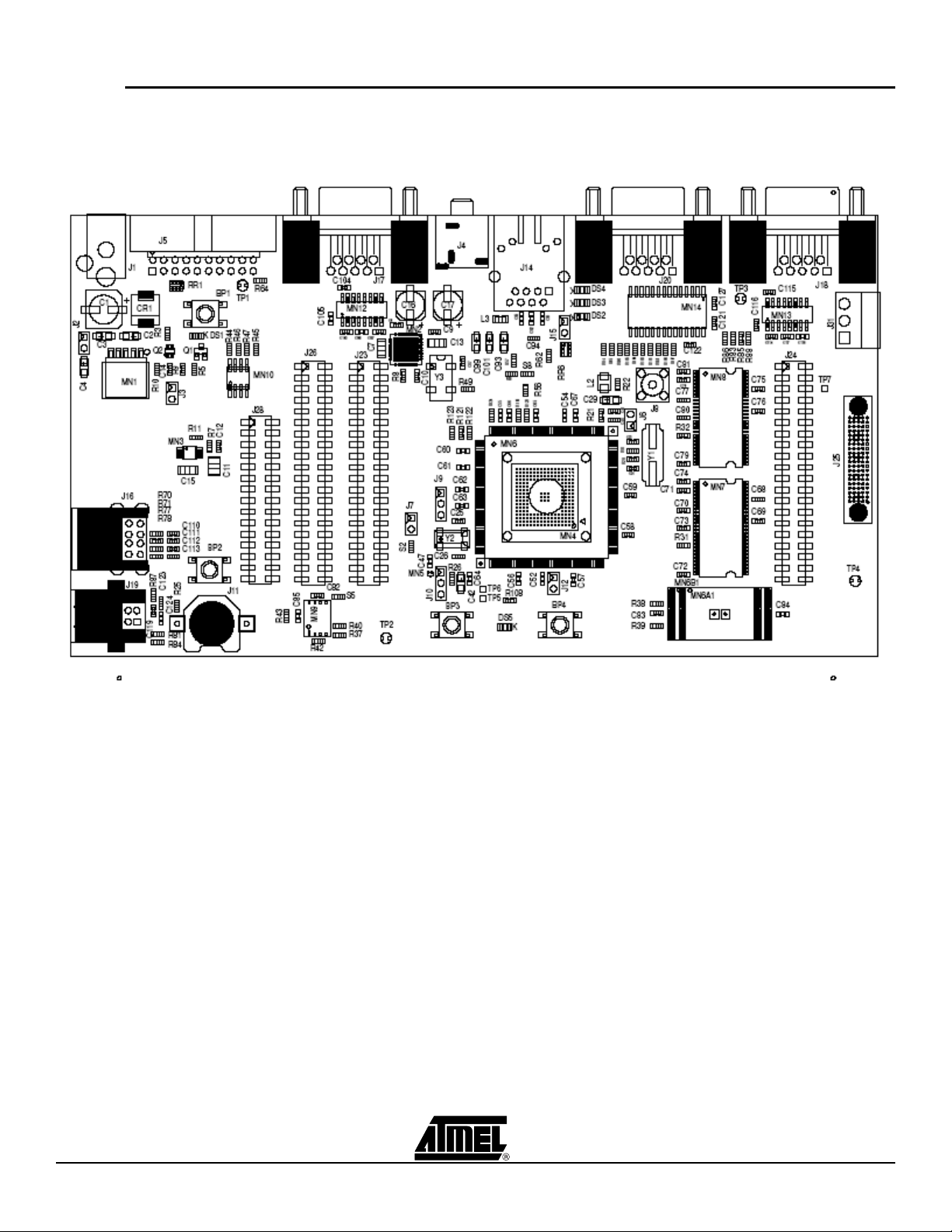
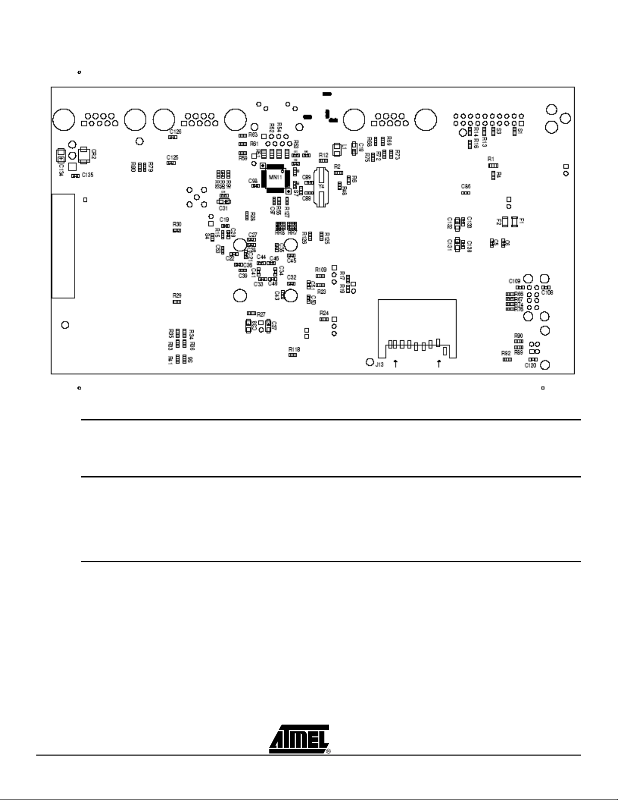
2.3 Layout
Figure 2-1. AT91SAM9260-EK Layout - Top View
2-2 AT91SAM9260-EK Evaluation Board User Guide
6234C–ATARM–22-Mar-07

Figure 2-2. AT91SAM9260-EK Layout - Bottom View
Setting Up the AT91SAM9260-EK Board
2.4 Powering Up the Board
2.5 Backup Power Supply
The AT91SAM9260-EK requires 5V DC (±5%). DC power is supplied to the board via
the 2.1 mm by 5.5 mm socket J1. Coaxial plug center positive standard.
The user has the possibility to plug a battery (3V Lithium Battery CR1225 or equivalent)
in order to permanently power the backup part of the device. In this case, J10 configuration must be set in position 1, 2.
Refer to Section 4.1.
2.6 Getting Started The AT91SAM9260-EK evaluation board is delivered with a CD-ROM containing all nec-
essary information and step-by-step procedures for working with the most common
development toolchains. Please refer to this CD-ROM, or to the AT91 web site,
http://www.atmel.com/products/AT91/, for the most up-to-date information on getting
started with the AT91SAM9260-EK.
AT91SAM9260-EK Evaluation Board User Guide 2-3
6234C–ATARM–22-Mar-07

Setting Up the AT91SAM9260-EK Board
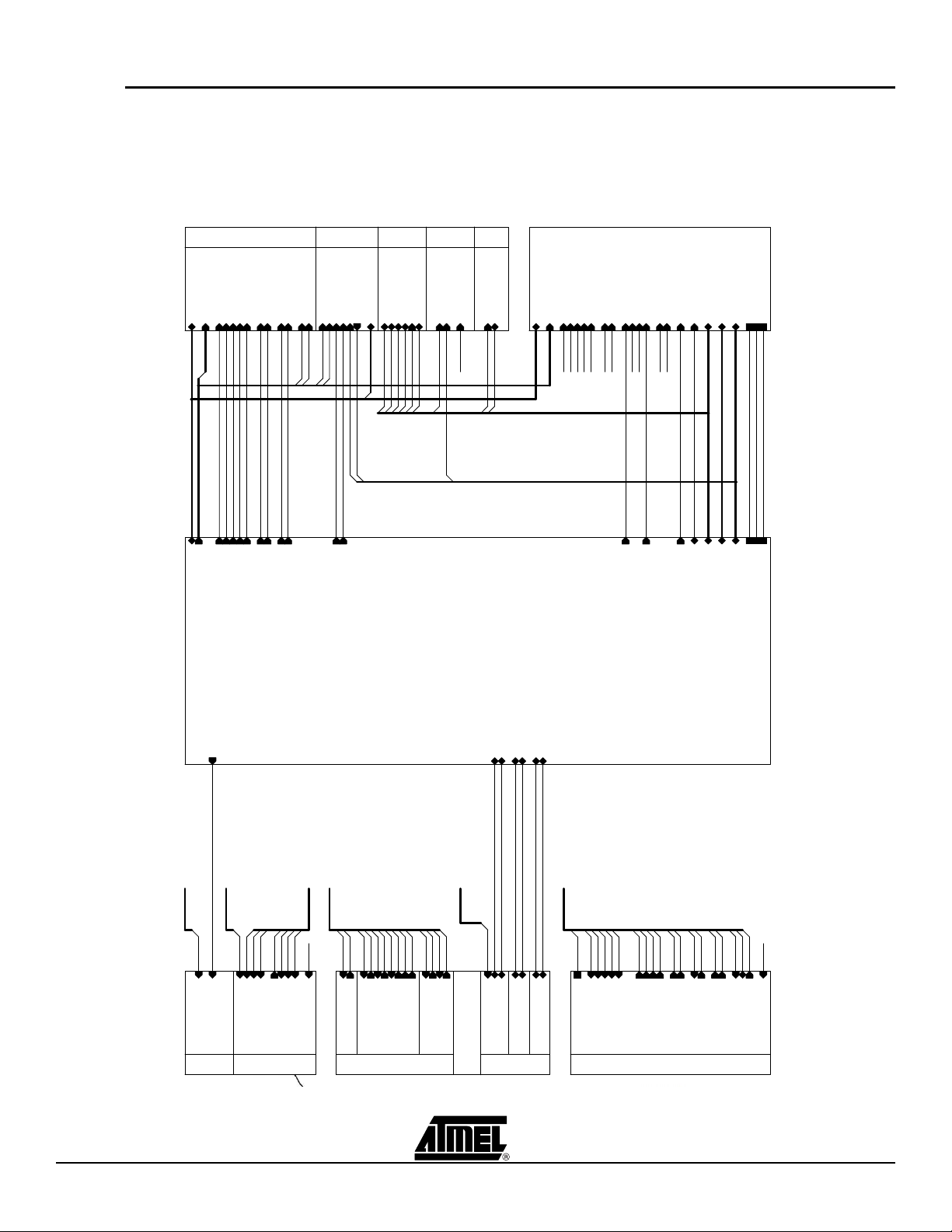
2.7 AT91SAM9260EK Block
Diagram
Figure 2-3. AT91SAM9260-EK Block Diagram
SDRAMNANFLASH
CAS
SDWE
SDCS_NCS1
SDCKE
CFIOR_NBS1_NWR1
SDCK
SDA10
D[0..31]
MEMORY
A[0..14]
RAS
CFIOW_NBS3_NWR3
NANDOE
ALE
CLE
BA0
BA1
NANDWE
RDYBSY
NANDCS
D[0..15]
DAT0
CARD
DAT1
DAT2
DATAFLASH
MCI
READER
CLK
DAT3
CMD
SCK
CS
DATAFLASH
SERIAL
NRST
SCL
EEPROM
SERIAL
SDA
03 - MEMORY
A[0..22]
D[0..31]
CAS
SDWE
SDCS_NCS1
SDA10
RAS
EXPANSION & User's Interfaces
SDCK
SDCKE
NANDOE
CFIOR_NBS1_NWR1
CFIOW_NBS3_NWR3
CFWE_NWE_NWR0
CFOE_NRD
NANDWE
NCS0
NRST
PA[0..31]
PB[0..31]
PC[0..15]
AVDD
VREFP
AGND
06 - EXPANSION CONNECTORS
AT91SAM9260
D[0..31]
A[0..22]
D[0..31]
A[0..14]
A[0..22]
RAS
SHDN
RAS
CAS
SDA10
CAS
SDA10
SDWE
SDCS_NCS1
SDWE
SDCS_NCS1
SDCK
SDCK
SDCKE
SDCKE
NBS1
NBS3
A16
A17
CFIOR_NBS1_NWR1
CFIOW_NBS3_NWR3
D[0..15]
NANDOE
NANDWE
A22
A21
PC14
PIO
NANDOE
NANDWE
PC13
PIO
PA0
PA5
PA4
PA3
PA8
MCCK
MCDB2
MCDB1
SPI0_MISO MCDB0
SPI0_NPCS0 MCDB3
PA1
SPI0_MOSI MCCDB
NRST
PC11
PA2
SPI0_SPCK
SPI0_NPCS1
PA23
TWD
TWCK
DDM
DDP
HDMA
HDPA
HDMB
HDPB
RAS
CAS
SDA10
SDWE
SDCS_NCS1
SDCK
SDCKE
NBS1
NBS3
NANDOE
CFOE_NRD
CFWE_NWE_NWR0
NANDWE
PB[0..31]
PA[0..31]
PC[0..15]
NRST
NCS0
NRST
PA[0..31]
PB[0..31]
PC[0..15]
AVDD
VREFP
AGND
02 - AT91SAM9260
PA[0..31]
PIO
PA9
POWER SUPPLY
SHDN
POWERLED
PC[0..15]
5VDC
PCK0
PC1
TD0
PB18
MCLK
TF0
PB17
SDIN
LRFS
TK0
PB16
BCLK
SPI1_NPCS0
SPI1_SPCK
SPI1_MOSI
SPI1_MISO
PB0
PB1
PB2
PB3
CS
DIN
CLK
DOUT
AT73C213
DAC
PB[0..31]
NRST
NRST
PB[0..31]
SERIAL INTERFACES
01 - POWER SUPPLY
DBGU_RXD
DBGU_TXD
PB15
PB14
DTXD
DRXD
DBGU
PC[0..15]
PIO
PB29
CTS1
RTS1
COM1
PC5 PA24
USBCNX
DDP
DDM
DEVICE
PB6
CTS0
PB24
DTR0
PB22
PB23
DSR0
PB25
DCD0
PB7
PB28
RI0
TXD1
RXD1
PB4
PB5
PB26
PB27
RTS0
TXD0
RXD0
COM0
RS232
HDPA
HDMA
HOST A
USB
HDPB
HDMB
HOST B
PA[0..31]
05 - COMMUNICATION
ETXCK/REFCLK
ETX3
PA19
PA11
TX_CLK
RMII_MII ETHERNET
TXD3
ETX2
PA10
TXD2
ETX1
PA13
TXD1
ETX0
PA12
ETXEN
PA16
TXD0
RX_ER
ECOL
PA29
COL
ECRS
PA28
CRS
EMDC
PA20
EMDIO
PA21
MDC
PIO
PA7
MDIO
NRST
NRST
MDINTR
ERX1
ERX0
ERXDV
PA14
RXD1
RXD0
ERXCK
PA17
PA27
RX_CLK
RX_DV
ETXER
PA22
TX_ER
ERXER
PA18
ERX2
ERX3
PA25
PA26
PA15
RXD2
RXD3
TX_EN
10/100 Mbps FAST ETHERNET
03 - RMII_MII ETHERNET
2-4 AT91SAM9260-EK Evaluation Board User Guide
6234C–ATARM–22-Mar-07

Section 3
Board Description
3.1 AT91SAM9260 Microcontroller
• Incorporates the ARM926EJ-S™ ARM® Thumb® Processor
– DSP Instruction Extensions, ARM Jazelle
– 8-KByte Data Cache, 8-KByte Instruction Cache, Write Buffer
– 200 MIPS at 180 MHz
– Memory Management Unit
– EmbeddedICE
• Additional Embedded Memories
– One 32-KByte Internal ROM, Single-cycle Access At Maximum Matrix Speed
– Two 4-KByte Internal SRAM, Single-cycle Access At Maximum Matrix Speed
• External Bus Interface (EBI)
– Supports SDRAM, Static Memory, ECC-enabled NANDFlash and CompactFlash
• USB 2.0 Full Speed (12 Mbits per second) Device Port
– On-chip Transceiver, 2,432-byte Configurable Integrated DPRAM
• USB 2.0 Full Speed (12 Mbits per second) Host Single Port in the 208-lead PQFP
Package and Double Port in 217-ball LFBGA Package
– Single or Dual On-chip Transceivers
– Integrated FIFOs and Dedicated DMA Channels
• Ethernet MAC 10/100 Base T
– Media Independant Interface or Reduced Media Independant Interface
– 28-byte FIFOs and Dedicated DMA Channels for Receive and Transmit
• Image Sensor Interface
– ITU-R BT. 601/656 External Interface, Programmable Frame Capture Rate
– 12-bit Data Interface for Support of High Sensibility Sensors
– SAV and EAV Synchronization, Preview Path with Scaler, YCbCr Format
• Bus Matrix
– Six 32-bit-layer Matrix
– Boot Mode Select Option, Remap Command
• Fully-featured System Controller, including
– Reset Controller, Shutdown Controller
– Four 32-bit Battery Backup Registers for a Total of 16 Bytes
– Clock Generator and Power Management Controller
– Advanced Interrupt Controller and Debug Unit
– Periodic Interval Timer, Watchdog Timer and Real-time Timer
• Reset Controller (RSTC)
– Based on a Power-on Reset Cell, Reset Source Identification and Reset Output
™
, Debug Communication Channel Support
®
Technology for Java® Acceleration
®
AT91SAM9260-EK Evaluation Board User Guide 3-1
6234C–ATARM–22-Mar-07

Board Description
Control
• Clock Generator (CKGR)
– Selectable 32768Hz Low-power Oscillator or Internal Low Power RC Oscillator on
Battery Backup Power Supply, Providing a Permanent Slow Clock
– 3 to 20 MHz On-chip Oscillator, One up to 240 MHz PLL and One up to 130 MHz
PLL
• Power Management Controller (PMC)
– Very Slow Clock Operating Mode, Software Programmable Power Optimization
Capabilities
– Two Programmable External Clock Signals
• Advanced Interrupt Controller (AIC)
– Individually Maskable, Eight-level Priority, Vectored Interrupt Sources
– Three External Interrupt Sources and One Fast Interrupt Source, Spurious
Interrupt Protected
• Debug Unit (DBGU)
– 2-wire UART and Support for Debug Communication Channel, Programmable
ICE Access Prevention
• Periodic Interval Timer (PIT)
– 20-bit Interval Timer plus 12-bit Interval Counter
• Watchdog Timer (WDT)
– Key-protected, Programmable Only Once, Windowed 16-bit Counter Running at
Slow Clock
• Real-time Timer (RTT)
– 32-bit Free-running Backup Counter Running at Slow Clock with 16-bit Prescaler
• One 4-channel 10-bit Analog-to-Digital Converter
• Three 32-bit Parallel Input/Output Controllers (PIOA, PIOB, PIOC)
– 96 Programmable I/O Lines Multiplexed with up to Two Peripheral I/Os
– Input Change Interrupt Capability on Each I/O Line
– Individually Programmable Open-drain, Pull-up Resistor and Synchronous Output
– High-current Drive I/O Lines, Up to 16 mA Each
• Peripheral DMA Controller Channels (PDC)
• One Two-slot MultiMedia Card Interface (MCI)
– SDCard/SDIO and MultiMediaCard
™
Compliant
– Automatic Protocol Control and Fast Automatic Data Transfers with PDC
• One Synchronous Serial Controller (SSC)
– Independent Clock and Frame Sync Signals for Each Receiver and Transmitter
– I²S Analog Interface Support, Time Division Multiplex Support
– High-speed Continuous Data Stream Capabilities with 32-bit Data Transfer
• Four Universal Synchronous/Asynchronous Receiver Transmitters (USART)
– Individual Baud Rate Generator, IrDA
®
Infrared Modulation/Demodulation,
Manchester Encoding/Decoding
– Support for ISO7816 T0/T1 Smart Card, Hardware Handshaking, RS485 Support
– Full Modem Signal Control on USART0
• Two 2-wire UARTs
• Two Master/Slave Serial Peripheral Interfaces (SPI)
– 8- to 16-bit Programmable Data Length, Four External Peripheral Chip Selects
– Synchronous Communications
• Two Three-channel 16-bit Timer/Counters (TC)
– Three External Clock Inputs, Two Multi-purpose I/O Pins per Channel
– Double PWM Generation, Capture/Waveform Mode, Up/Down Capability
3-2 AT91SAM9260-EK Evaluation Board User Guide
6234C–ATARM–22-Mar-07
 Loading...