


ASUS PI-XP55T2P4 User Manual

R
P/I-XP55T2P4
Pentium Motherboard
USER'S MANUAL

USER'S NOTICE
No part of this product, including the product and software may be reproduced,
transmitted, transcribed, stored in a retrieval system, or translated into any language in any form by any means without the express written permission of ASUST eK
COMPUTER INC. (hereinafter referred to as ASUS) except documentation kept
by the purchaser for backup purposes.
ASUS provides this manual "as is" without warranty of any kind, either express or
implied, including but not limited to the implied warranties or conditions of merchantability or fitness for a particular purpose. In no event shall ASUS be liable for
any loss or profits, loss of business, loss of use or data, interruption of business, or
for indirect, special, incidental, or consequential damages of any kind, even if ASUS
has been advised of the possibility of such damages arising from any defect or error
in this manual or product. ASUS may revise this manual from time to time without
notice.
Products mentioned in this manual are mentioned for identification purposes only.
Product names appearing in this manual may or may not be registered trademarks
or copyrights of their respective companies.
The product name and revision number are both printed on the board itself. Manual
revisions are released for each board design represented by the digit before and
after the period of the manual revision number . Manual updates are represented by
the third digit in the manual revision number . For updated BIOS, drivers, or product release information you may visit ASUS' home page at: http://www .asus.com.tw/
© Copyright 1996 ASUSTeK COMPUTER INC. All rights reserved.
Product Name: P/I-XP55T2P4
Manual Revison: 3.00
Manual Release: October 1996
II
ASUS P/I-XP55T2P4 User's Manual

ASUS CONTACT INFORMATION
ASUSTeK COMPUTER INC.
Marketing Info:
Address: 150 Li-Te Road, Peitou, Taipei, Taiwan, ROC
Telephone: 886-2-894-3447
Fax: 886-2-894-3449
Email: info@asus.com.tw
Technical Support:
Fax: 886-2-895-9254
BBS: 886-2-896-4667
Email: tsd@asus.com.tw
WWW: http://www.asus.com.tw/
Gopher: gopher.asus.com.tw
FTP: ftp.asus.com.tw/pub/ASUS
ASUS COMPUTER INTERNATIONAL
Marketing Info:
Address: 721 Charcot Avenue, San Jose, CA 95131, USA
Telephone: 1-408-474-0567
Fax: 1-408-474-0568
Email: info-usa@asus.com.tw
Technical Support:
BBS: 1-408-474-0569
Email: tsd-usa@asus.com.tw
ASUS COMPUTER GmbH
Marketing Info:
Address: Harkort Str. 25, 40880 Ratingen, BRD, Germany
Telephone: 49-2102-445011
Fax: 49-2102-442066
Email: info-ger@asus.com.tw
Technical Support:
BBS: 49-2102-448690
Email: tsd-ger@asus.com.tw
ASUS P/I-XP55T2P4 User's Manual III

CONTENTS
I. INTRODUCTION........................................................1
How this manual is organized..........................................................1
Item Checklist ..................................................................................1
Features of This Motherboard..........................................................2
II. FEATURES.................................................................2
Parts of the Motherboard .................................................................3
III. INSTALLATION .......................................................4
Map of the ASUS Motherboard .......................................................4
Jumpers.................................................................................5
Expansion Slots ....................................................................5
Connectors ............................................................................5
Installation Steps..............................................................................6
1. Jumpers ........................................................................................6
Jumper Settings ....................................................................7
2. System Memory (DRAM & SRAM)........................................12
TAG SRAM Upgrade: ........................................................12
DRAM Memory Installation Procedures: ..........................13
Static RAM (SRAM) for Level 2 (External) Cache ......................14
Compatible Cache Modules for this Motherboard .............14
3. Central Processing Unit (CPU).................................................15
4. Expansion Cards .......................................................................16
Expansion Card Installation Procedure: .............................16
Assigning IRQs for Expansion Cards.................................16
Assigning DMA Channels for ISA Cards...........................17
ASUS MediaBus Card........................................................18
5. External Connectors..................................................................19
Power Connection Procedures............................................25
Support Software......................................................................25
IV. BIOS SOFTWARE ..................................................26
6. BIOS Setup ...............................................................................26
Load Defaults .....................................................................27
Standard CMOS Setup .............................................................27
Details of Standard CMOS Setup:......................................28
IV
ASUS P/I-XP55T2P4 User's Manual

CONTENTS
BIOS Features Setup ................................................................30
Details of BIOS Features Setup:.........................................31
Chipset Features Setup .............................................................33
Power Management Setup........................................................36
Details of Power Management Setup: ................................37
PNP and PCI Setup ..................................................................39
Load BIOS Defaults .................................................................40
Load Setup Defaults .................................................................41
Supervisor Password and User Password ................................41
IDE HDD Auto Detection ........................................................43
Save and Exit Setup .................................................................44
Exit Without Saving .................................................................44
Flash Memory Writer Utility .........................................................45
The Flash Memory Writer Utility Screen:..........................46
V. DESKTOP MANAGEMENT...................................49
Desktop Management Interface (DMI)..........................................49
Introducing the DMI Configuration Utility ........................49
System Requirements .........................................................49
Using the DMI Configuration Utility .................................50
Notes:..................................................................................50
VI. PCI-SC200 SCSI Card............................................53
NCR SCSI BIOS and Drivers ........................................................53
The PCI-SC200 SCSI Interface Card ............................................54
Setting Up the PCI-SC200 .......................................................54
Setting the INT Assignment .....................................................55
Terminator Settings ..................................................................55
SCSI ID Numbers ....................................................................56
VII. I-A16C Audio Card ...............................................57
I-A16C Audio Features ............................................................57
Unpacking and Handling Precautions ......................................57
Layout and Connectors ............................................................58
Connectors ..........................................................................58
VIII. DOS 3.1 & Windows 3.1x Audio Software
(with optional I-A16C Audio Card Bundle Only)
IX. Windows 95 Audio Software
(with optional I-A16C Audio Card Bundle Only)
ASUS P/I-XP55T2P4 User's Manual V

FCC & DOC COMPLIANCE
Federal Communications Commission Statement
This device complies with FCC Rules Part 15. Operation is subject to the following
two conditions:
• This device may not cause harmful interference, and
• This device must accept any interference received, including interference that
may cause undesired operation.
This equipment has been tested and found to comply with the limits for a Class B
digital device, pursuant to Part 15 of the FCC Rules. These limits are designed to
provide reasonable protection against harmful interference in a residential installation. This equipment generates, uses and can radiate radio frequency energy and, if
not installed and used in accordance with manufacturer's instructions, may cause
harmful interference to radio communications. However, there is no guarantee that
interference will not occur in a particular installation. If this equipment does cause
harmful interference to radio or television reception, which can be determined by
turning the equipment off and on, the user is encouraged to try to correct the interference by one or more of the following measures:
• Re-orient or relocate the receiving antenna.
• Increase the separation between the equipment and receiver.
• Connect the equipment to an outlet on a circuit different from that to which
the receiver is connected.
• Consult the dealer or an experienced radio/TV technician for help.
WARNING: The use of shielded cables for connection of the monitor to the graphics
card is required to assure compliance with FCC regulations. Changes or modifications to this unit not expressly approved by the party responsible for compliance
could void the user's authority to operate this equipment.
Canadian Department of Communications Statement
This digital apparatus does not exceed the Class B limits for radio noise emissions
from digital apparatus set out in the Radio Interference Regulations of the Canadian Department of Communications.
VI
ASUS P/I-XP55T2P4 User's Manual

I. INTRODUCTION
How this manual is organized
This manual is divided into the following sections:
I. Introduction: Manual information and checklist
II. Features: Information and specifications
III. Installation: Instructions on setting up the motherboard
IV. BIOS Setup: BIOS software setup information
V. ASUS DMI Utility: BIOS supported Desktop Management Interface
VI. ASUS PCI-SC200: Installation of an optional SCSI card
VII. ASUS I-A16C: Installation of an optional Audio card
VIII. DOS/Win3.1x: Audio Software Manual (with I-A16C bundle only)
IX. Windows 95: Audio Software Manual (with I-A16C bundle only)
Item Checklist
Please check that your package is complete. If you discover damaged or missing
items, please contact your retailer.
I. INTRODUCTION
(Manual / Checklist)
√ The ASUS P/I-XP55T2P4 motherboard with built-in 2 serial, 1 parallel,
PS/2 Keyboard, and PS/2 Mouse connectors
√ 1 IDE ribbon cable
√ 1 floppy ribbon cable
√ Support software (view FILELIST.TXT detailed contents and description)
• Bus Master IDE Drivers
• PFLASH BIOS Utility
√ This user's manual (audio sections included with I-A16C bundle only)
Optional infrared module
Optional ASUS PCI-SC200 Fast-SCSI card
Optional ASUS I-A16C Audio Card
ASUS P/I-XP55T2P4 User's Manual 1

II. FEATURES
(Features)
II. FEATURES
Features of This Motherboard
The ASUS P/I-XP55T2P4 is carefully designed for the demanding PC user who
wants a great many features in a small package. This motherboard:
• Easy Installation: Is equipped with BIOS that supports auto detection of hard
drives and Plug and Play to make setup of hard drives and expansion cards
virtually automatic.
• Multi-Processor/Multi-Speed Support: Supports one Pentium (75-200MHz),
Cyrix P166+ (Rev 2.7 or later), or AMD-K5 (PR75-100MHz) (See page 11).
• Intel Chipset: Features Intel's 430HX PCIset with I/O subsystems.
• Error Checking and Correcting (ECC): Using Intel's 430HX PCIset and
parity DRAM modules can detect multi-bit errors and correct 1-bit memory
errors.
• Desktop Management Interface (DMI): Supports DMI through BIOS which
allows hardware to communicate within a standard protocol creating a higher
level of compatibility. (See section V)
• ATX Power Connector: Has a single easy-to-install connector for 3.3V, 5V,
12V, and a new soft-power control. (Requires an ATX power supply)
• L2 Cache: Provides the option of 0KB upgradeable to 256KB or 512KB,
onboard 256KB upgradeable to 512KB, or 512KB onboard Pipelined Burst
SRAM. Upgrades are made through a Synchronous SRAM cache module.
(See page 14 for compatible cache modules.)
• V ersatile DRAM Memory Support: Supports 72-pin SIMMs of 4MB, 8MB,
16MB, 32MB, or 64MB to form a memory size between 8MB to 256MB.
Supports both Fast Page Mode (FPM) and Extended Data Output (EDO)
SIMMs. (see page 12)
• ISA and PCI Expansion Slots: Provides four 16-bit ISA slots, three 32-bit
PCI slots, and one PCI/MediaBus 2.0 which allows the use of either an standard PCI card or the ASUS MediaBus Card.
• ASUS MediaBus Rev 2.0: Features an expansion slot extension shared with
PCI Slot 4 for an optional high-performance expansion card which includes
two functions in one easy-to-install card. (For revision compatibility infor-
mation, please refer to page 18.)
• Super Multi-I/O: Provides two high-speed UART compatible serial ports
and one parallel port with EPP and ECP capabilities. UART2 can also be
directed from COM2 to the Infrared Module for wireless connections. Two
floppy drives of either 5.25" or 3.5" (1.44MB or 2.88MB) are also supported
without an external card. The Japanese "Floppy 3 mode" (3.5" 1.2MB)
floppy standard is also supported.
• NCR SCSI BIOS: This motherboard has firmware that supports the optional
ASUS PCI-SC200 SCSI controller cards.
2 ASUS P/I-XP55T2P4 User's Manual
II. FEATURES
• PCI Bus Master IDE Controller: Comes with an onboard PCI Bus Master
IDE controller with two connectors that supports four IDE devices in two channels, provides faster data transfer rates, and supports Enhanced IDE devices
such as T ape Backup and CD-ROM drives. This controller supports PIO Modes
3 and 4 and Bus Master IDE DMA Mode 2. BIOS supports IDE CD-ROM
or SCSI boot-up.
• Optional IrDA: This motherboard supports an optional infrared port module
for wireless interface.
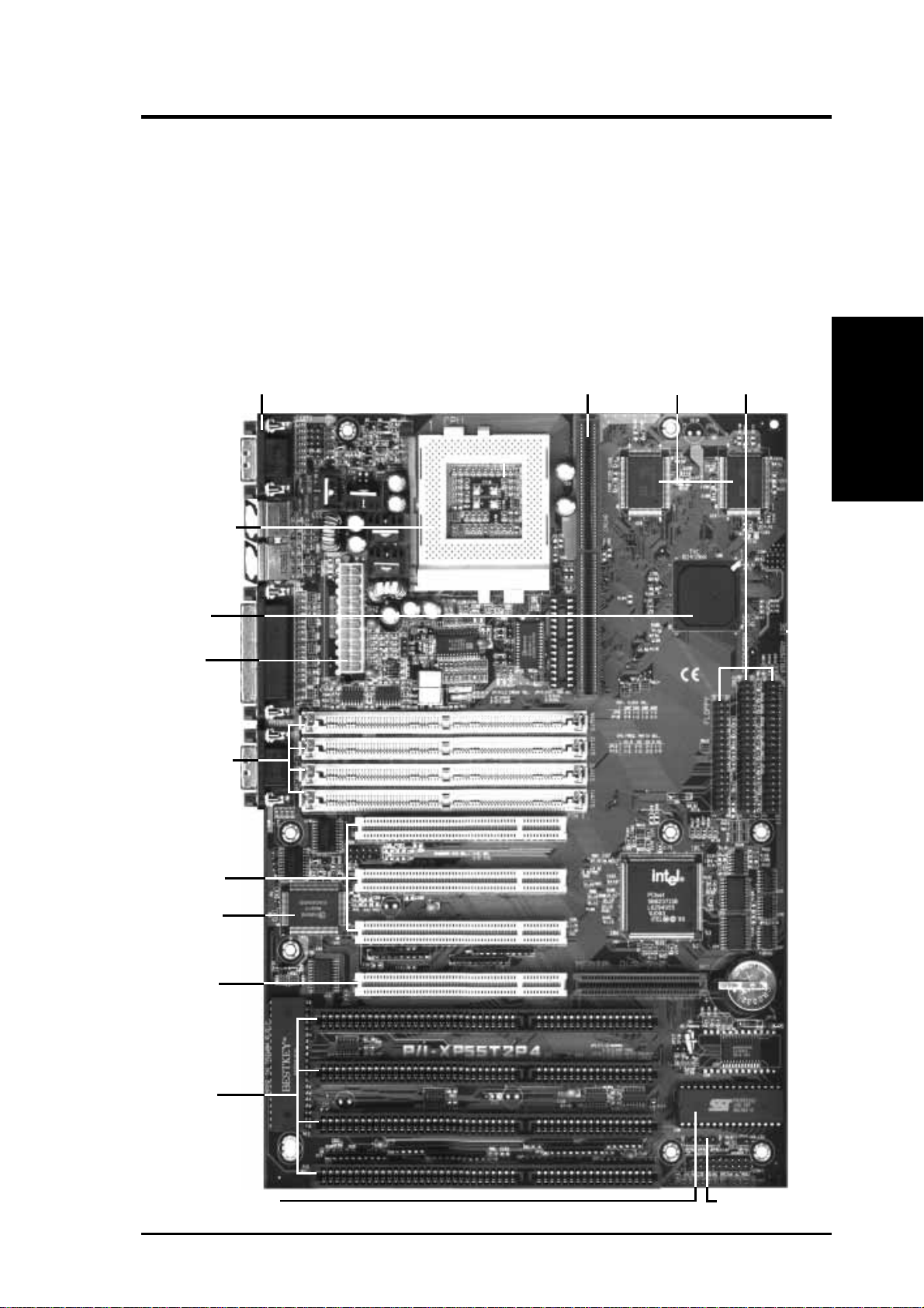
Parts of the Motherboard
CPU ZIF Socket 7
Intel's 430HX
PCIset
ATX Power
(4) 72-pin SIMM
Sockets
L2 Upgrade Cache
Expansion Slot
Onboard 256KB/
512KB Pipelined
Burst L2 Cache
Floppy & IDESerial, Parallel, PS/2 Mouse, PS/2 Keyboard
II. FEATURES
(Parts of Board)
(3) PCI Slots
Super Multi-I/O
PCI 4 or ASUS
MediaBus 2.0
(4) ISA Slots
Programmable Flash ROM
Infrared Port
ASUS P/I-XP55T2P4 User's Manual 3
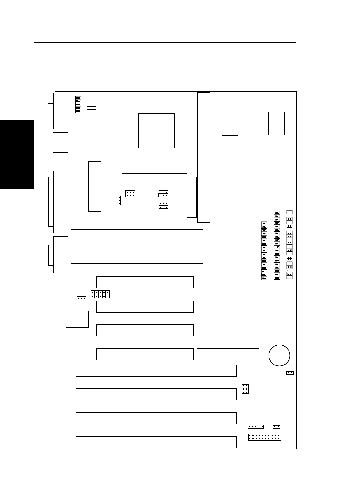
Map of the ASUS Motherboard
III. INSTALLATION
(Map of Board)
CPU Vcore Volt (2.5-2.9)
2.5
2.7
2.8
2.9
Res.
COM 1
PS/2
Mouse
PS/2
Key-
board
JP1
CPU Volt (STD/VRE)
III. INSTALLATION
256KB/512KB Onboard L2 Cache
CPU ZIF Socket 7
Board Power Input
for ATX Power Supply
Parallel PrinterCOM 2
SIMM Socket 4 (Bank 1)
SIMM Socket 3 (Bank 1)
SIMM Socket 2 (Bank 0)
SIMM Socket 1 (Bank 0)
PCI Slot 1
JP16
Multi-I/O (En/Dis)
PCI Slot 2
Super
Multi-I/O
PCI Slot 3
PCI Slot 4
Bus Freq.
L2 Cache (256/512)
CPU Fan Power
Memory Cached (64/512)
Universal Serial Bus
JP9
JP10
Freq. Ratio
JP12
JP13
JP14
JP15
Tag SRAM Upgrade
Pipelined Burst Level 2 Cache Expansion Slot
Floppy Drives
Secondary IDE
Primary IDE
CR2032
MediaBus 2.0
3 Volt
Lithium Cell
ISA Slot 1
ISA Slot 2
ISA Slot 3
ISA Slot 4
4 ASUS P/I-XP55T2P4 User's Manual
Block Write (Dis/En)
CMOS (Operate/Clear)
JP17
JP18
IR Conn
Case Connector
JP19
IDE LED

III. INSTALLATION
Jumpers
1) JP14 p. 7 Total Level 2 Cache Size Setting (256KB/512KB)
2) JP18 p. 7 Flash ROM Boot Block Program (Enable/Disable)
3) JP15 p. 8 Memory Cacheable Size (64MB/512MB)
4) JP16 p. 8 SMC37C669 Multi-I/O Selection (Enable/Disable)
5) JP17 p. 9 CMOS RAM (Operation/Clear CMOS Data)
6) JP19 p. 9 Battery Test Jumper (Operation/Test Mode)
7) JP9, JP10 p. 10 CPU External Clock (BUS) Frequency Selection
8) JP12, JP13 p. 10 CPU:BUS Frequency Ratio
9) JP1 p. 11 Single Power Plane Voltage Regulator (STD/VRE)
10) Vcore p. 11 Dual Power Plane Voltage Regulator (2.5V-2.9V)
Expansion Slots
1) SIMM Slots p. 12 DRAM Memory Expansion slots
2) TAG SRAM p. 12 Upgrade socket for TAG SRAM
3) Cache Expansion p. 14 Socket for Pipelined Burst SRAM Cache Module
4) ZIF Socket 7 p. 15 Socket for Central Processing Unit (CPU)
5) ISA Slots 1, 2, 3, 4 p. 16 16-bit ISA Bus Expansion slots
6) PCI Slots 1, 2, 3 p. 16 32-bit PCI Bus Expansion slots
7) PCI 4 / MediaBus p. 18 32-bit PCI Bus Slot and MediaBus
(Map of Board)
III. INSTALLATION
Connectors
1) PS/2 Keyboard p. 19 PS/2 Keyboard connector (6-pin female)
2) PS/2 Mouse p. 19 PS/2 Mouse connector (6-pin female)
3) Parallel Port p. 19 Parallel Port connector (25-pin female)
4) Serial Port p. 19 Serial Port COM1 & COM2 (9-pin male)
5) ATX Power Input p. 20 Motherboard ATX Power connector (20-pin Block)
6) Primary/Second IDE p. 21 Primary/Secondary IDE connectors (40-pin Blocks)
7) Floppy Drive p. 21 Floppy Drive connector (34-pin Block)
8) IDE_LED p. 22 IDE_LED activity light
9) Power LED (CON1) p. 22 System Power LED (2-pins)
10) Key Lock (CON1) p. 22 Keyboard Lock Switch lead (5-pins)
11) SMI Switch (CON1) p. 22 SMI Switch lead (2-pins)
12) ATX Power (CON1) p. 23 Power switch for ATX power supply only
13) Reset Switch (CON1) p. 23 Reset Switch lead (2-pins)
14) Speaker (CON1) p. 23 Speaker connector (4-pins)
15) FAN p. 24 CPU 12V Cooling Fan connector
16) IR CON p. 24 Infrared Port Module connector
ASUS P/I-XP55T2P4 User’s Manual 5
III. INSTALLATION
Pin 1
Installation Steps
Before using your computer, you must complete the following steps:
1. Set Jumpers on the Motherboard
2. Install DRAM and SRAM Modules
3. Install the Central Processing Unit (CPU)
4. Install Expansion Cards
5. Connect Ribbon Cables, Cabinet Wires, and Power Supply
6. Setup the BIOS Software
1. Jumpers
Several hardware settings are made through the use of jumper caps to connect jumper
pins (JP) on the motherboard. See "Map of the Motherboard" on page 4 for loca-
III. INSTALLATION
(Jumpers)
tions of jumpers. The jumper settings will be described numerically such as [----],
[1-2], [2-3] for no connection, connect pins 1&2, and connect pins 2&3 respec-
Pin 1
tively. Pin 1 for our motherboards is always on top
holding the motherboard with the keyboard connector away from yourself. A "1" is
written besides pin 1 on jumpers with three pins. The jumpers will also be shown
graphically such as
Jumpers with two pins will be shown as
For manufacturing simplicity, the jumpers may be sharing pins from other groups.
Use the diagrams in this manual instead of following the pin layout on the board.
Settings with two jumper numbers require that both jumpers be moved together . To
connect the pins, simply place a plastic jumper cap over the two pins as diagramed.
WARNING: Computer motheboards and components contain very delicate
Integrated Circuit (IC) chips. To protect the motherboard and other components against damage from static electricity, you should follow some precautions whenever you work on your computer.
1. Unplug your computer when working on the inside.
2. Hold components by the edges and try not to touch the IC chips, leads, or
circuitry.
3. Use a grounded wrist strap before handling computer components.
4. Place components on a grounded antistatic pad or on the bag that came with
the component whenever the components are separated from the
system.
to connect pins 1&2 and to connect pins 2&3.
for short (On) and for open (Off).
or on the left
when
6 ASUS P/I-XP55T2P4 User’s Manual
III. INSTALLATION
Jumper Settings
1. Total Level 2 Cache Size Setting (JP14)
This jumper sets the total amount of L2 cache that is present. If you have both
onboard cache chips (see "Map of Motherboard" for locations) and a Cache
Expansion Slot, then you have 256KB. If you only have onboard cache chips,
then you have 512KB. An "ASUS" or "COAST" cache module can be used to
upgrade the 256KB version to 512KB. If there is no onboard cache, you may
install a cache module of either 256KB or 512KB. IMPORTANT: See page
14 "SRAM Cache" for installation procedures. Regardless of your cache
combination, set the following jumpers according to the total amount of L2
cache that is present onboard and installed as a module.
Cache Size JP14
256KB [1-2]
512KB [2-3]
JP14
1
2
3
256KB
Total L2 Cache Size Setting (256KB / 512KB)
JP14
1
2
3
512KB
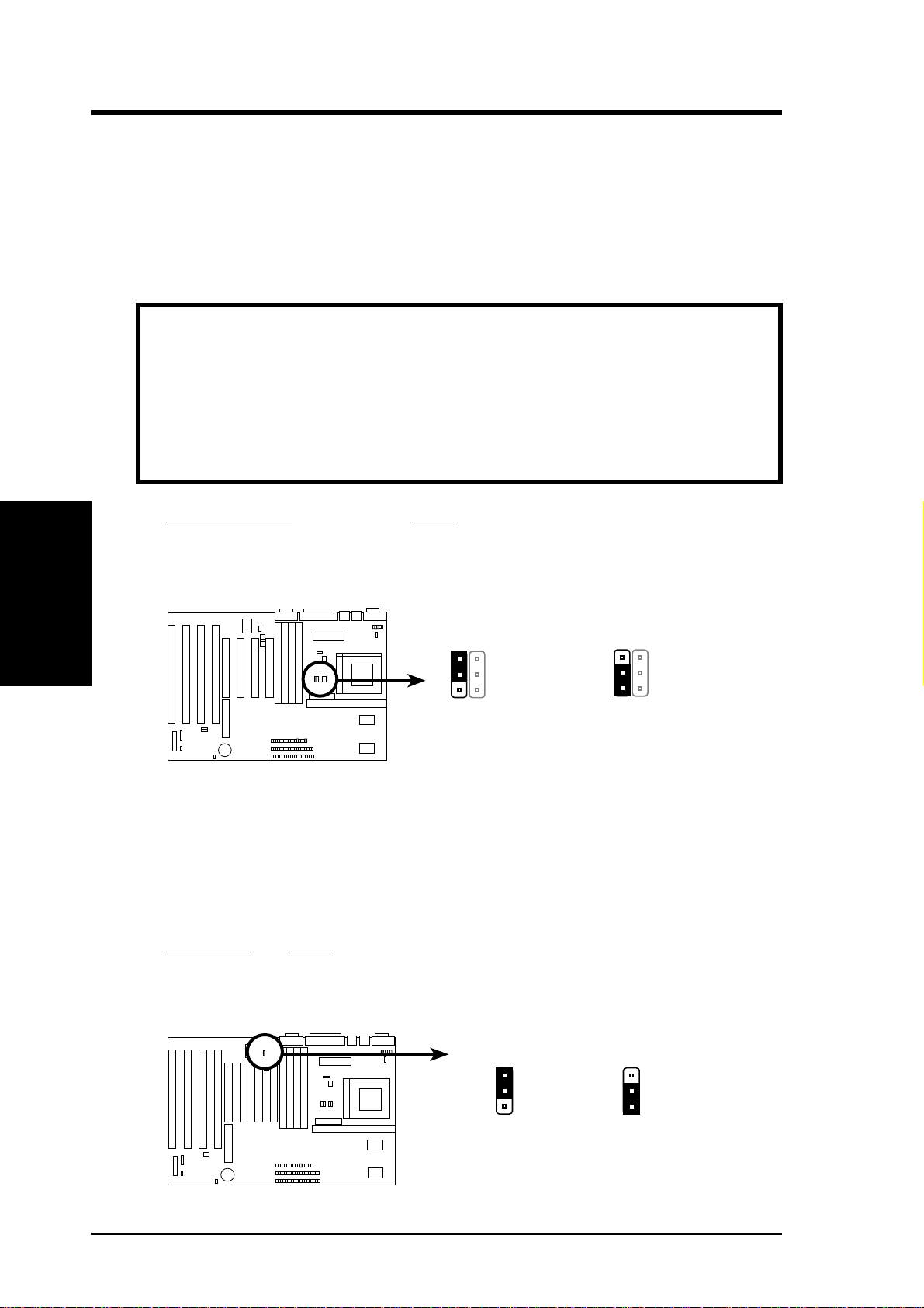
2. Flash ROM Boot Block Programming (JP18)
This sets the operation mode of the boot block area of the BIOS Flash ROM to
allow programming in the Enabled position.
Programming JP18
Disabled [1-2] (Default)
Enabled [2-3]
123
123
(Jumpers)
III. INSTALLATION
JP18
Disabled (Default) Enabled
Boot Block Programming (Disable / Enable)
JP18
ASUS P/I-XP55T2P4 User’s Manual 7
III. INSTALLATION
3. Memory Cacheable Size (JP15)
The default of 64MB uses only the onboard T AG SRAM which allows cacheable
memory up to 64MB. If you install DRAM above 64MB and wish to allow
cacheable memory above 64MB, you need to install a TAG SRAM upgrade or
use a cache module with an extended TAG SRAM (such as 256KB ASUS CM1
Rev 3.0 with 2 TAG SRAM's) but not both and set this jumper to 512MB. See
page 12 for TAG SRAM upgrade and page 14 for cache module information.
WARNING: If there are DRAM cache chips (MCache) either onboard or on
the SIMM cache module instead of pipelined burst SRAM chips, this jumper
must be set to 64MB. 512MB will make the system unstable. Mcache chips
can only allow cacheable memory up to 64MB. See "Map of Motherboard" on
page 4 for L2 cache locations. If the cache module that you install already
have an extended tag, do not install another TAG SRAM into the T AG SRAM
Upgrade Socket.
III. INSTALLATION
(Jumpers)
Cacheable Size JP15
64MB (BSRAM/MCache) [1-2] (Default)
512MB (BSRAM Only) [2-3]
JP15
1
2
3
64MB Cacheable (Default)
Burst SRAM or MCache
Memory Cacheable Size (64MB/512MB)
JP15
1
2
3
512MB Cacheable
Burst SRAM Only
4. Onboard Multi-I/O Selection (JP16)
You can selectively disable each onboard Multi-I/O item (floppy, serial, parallel, and IrDA) through BIOS (see pages 35 & 36) or disable all Multi-I/O items
at once with the following jumper in order to use your own Multi-I/O card.
Selections JP16
Enable [1-2] (Default)
Disable [2-3]
JP16
1
2
3
Enable (Default) Disabled
Multi I/O Setting (Enable / Disable)
8 ASUS P/I-XP55T2P4 User’s Manual
JP16
1
2
3
III. INSTALLATION
5. CMOS RAM (JP17)
This clears the user-entered information stored in the CMOS RAM of the Real
Time Clock such as hard disk information and passwords. To clear the CMOS
data: (1) T urn off the PC, (2) Set jumper to "Clear ," (3) Power on the PC, (4) T urn
off the PC, (5) Set jumper to "Operation," (6) Power on the PC, (7) Hold down
<Delete> during bootup and enter BIOS setup to re-enter user information.
Selections JP17
Operation [1-2] (Default)
Clear CMOS Data [2-3] (momentarily)
123
JP17
Operation (Default) Clear CMOS Data
CMOS RAM (Operation / Clear CMOS Data)
123
JP17
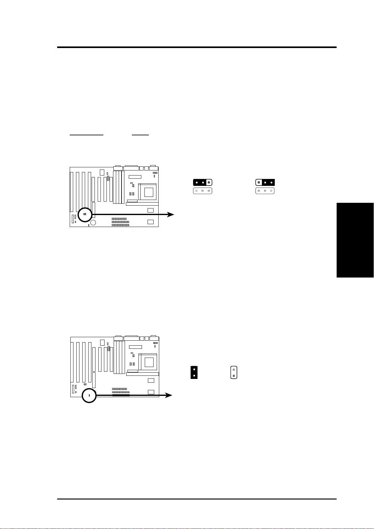
6. Battery Test Jumper (JP19)
The CMOS RAM is powered by the onboard button cell battery. You can test
the battery’s current by removing this jumper and attaching a current meter to
each pin. WARNING: You must unplug the power cord to your power
supply to ensure that there is no power to your motherboard. The CMOS
RAM containing BIOS setup information will be cleared by this action.
Y ou must enter BIOS to “Load Setup Defaults” and re-enter any user information after removing and reapplying this jumper.
(Jumpers)
III. INSTALLATION
JP19
Operation Test Mode
Battery Test Jumper
JP19
ASUS P/I-XP55T2P4 User’s Manual 9
III. INSTALLATION
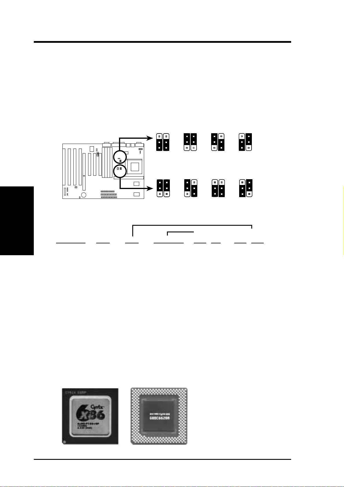
7. CPU External Clock (BUS) Frequency Selection (JP9, JP10)
These jumpers tells the clock generator what frequency to send to the CPU to allow
the selection of the CPU’s External frequency (or BUS Clock). The BUS Clock
times the BUS Ratio equals the CPU's Internal frequency (the advertised CPU speed).
8. CPU to BUS Frequency Ratio (JP12, JP13)
These jumpers set the frequency ratio between the Internal frequency of the CPU
and the External frequency (called the BUS Clock) within the CPU. These must
be set together with the above jumpers CPU External (BUS) Frequency Selection.
JP10
JP9
JP10
JP9
JP10
JP9
JP10
JP9
III. INSTALLATION
(Jumpers)
55MHz
JP12
JP13
1
2
3
1
2
3
1
2
3
50MHz
CPU External Clock (BUS) Frequency Selection
JP12
JP13
1
2
3
1.5 x 2.0 x 2.5 x 3.0 x
CPU : BUS Frequency Ratio (1.5x, 2.0x, 2.5x, 3.0x)
60MHz
JP12
JP13
1
2
3
1
2
3
66MHz
JP12
JP13
1
2
3
1
2
3
Set the jumpers by the Internal speed of the Intel, AMD, or Cyrix CPU’s as follows:
(BUS Freq.) (Freq. Ratio)
CPU Model Freq. Ratio (BUS Freq.) JP10 JP9 JP13 JP12
Intel Pentium 200MHz 3.0x 66MHz [2-3] [1-2] [2-3] [1-2]
Intel Pentium 166MHz 2.5x 66MHz [2-3] [1-2] [2-3] [2-3]
Intel Pentium 150MHz 2.5x 60MHz [1-2] [2-3] [2-3] [2-3]
Intel Pentium 133MHz 2.0x 66MHz [2-3] [1-2] [1-2] [2-3]
Intel Pentium 120MHz 2.0x 60MHz [1-2] [2-3] [1-2] [2-3]
Intel Pentium 100MHz 1.5x 66MHz [2-3] [1-2] [1-2] [1-2]
Intel Pentium 90MHz 1.5x 60MHz [1-2] [2-3] [1-2] [1-2]
Intel Pentium 75MHz 1.5x 50MHz [2-3] [2-3] [1-2] [1-2]
AMD 100MHz 1.5x 66MHz [2-3] [1-2] [1-2] [1-2]
AMD 90MHz 1.5x 60MHz [1-2] [2-3] [1-2] [1-2]
AMD 75MHz 1.5x 50MHz [2-3] [2-3] [1-2] [1-2]
*Cyrix 166+ 133MHz 2.0x 66MHz [2-3] [1-2] [1-2] [2-3]
*The only Cyrix CPU that is supported on this motherboard is labeled Cyrix 6x86
P166+ but must be Revision 2.7 and later. Look on the underside of the CPU for the
serial number. The number should read G8DC6620A or larger.
10 ASUS P/I-XP55T2P4 User’s Manual
III. INSTALLATION
9-10. Single/Dual Power Plane CPU Voltage Regulator Selections
The following jumpers set the voltage supplied to the CPU. Determine whether
your CPU has a Single Power Plane or Dual Power Planes and then the voltage that it uses. When a single power plane CPU is installed, the dual power
plane selections will be automatically disabled. When a dual power plane CPU
is installed, the single power plane selections will be automatically disabled.
You may have one jumper on the Single Power Plane and another on the Dual
Power Planes at the same time.
9. Single Power Plane CPU Voltage Regulator Selection (JP1)
These jumpers set the voltage supplied to single power plane CPU's. For ex-
ample most CPU’ s only have a single power plane and use the standard voltage
setting but currently Cyrix 6x86 166+ Rev 2.7, AMD K586-100, and Intel Pentium
166&200 CPU’s use the VRE setting. WARNING: You can damage your
CPU if you are not exactly clear on CPU jumper settings, check with your
retailer before using your system.
Single Power Plane JP1
STD 3.3V-3.465V [1-2] (Default)
VRE 3.4V-3.6V [2-3]
JP1
1
2
3
STD 3.3V - 3.465V (Default)
Voltage Regulator Output Selection (STD / VRE)
JP1
1
2
3
VRE 3.4-3.6V
10. Dual Power Plane CPU Voltage Regulator Selection
These jumpers set the voltage supplied to dual power plane CPU's.
WARNING: Position [9-10] is reserved for future use, do not use this setting or you may cause damage to your CPU.
Dual Power Planes [9-10] [7-8] [5-6] [3-4] [1-2]
Reserved 2.9V 2.8V 2.7V 2.5V
(Jumpers)
III. INSTALLATION
2.8V
2.7V
2.5V
Res.
2.9V
2.8 Volt Default
CPU Vcore Voltage Selection
ASUS P/I-XP55T2P4 User’s Manual 11
III. INSTALLATION
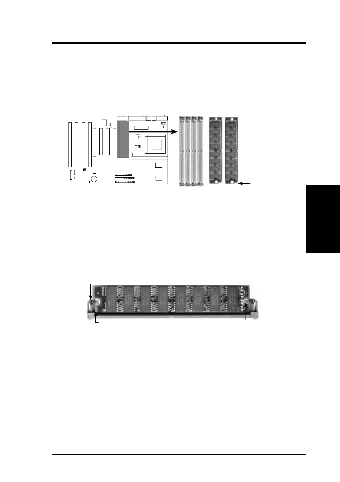
2. System Memory (DRAM & SRAM)
This motherboard supports four 72-pin SIMMs of 4MB, 8MB, 16MB, 32MB, or
64MB to form a memory size between 8MB to 256MB. The DRAM can be either
60ns or 70ns Fast Page Mode (Asymmetric or Symmetric) or EDO. To support
ECC, you must use true (opposed to phantom parity generated by logic chips) 36-bit
parity-type DRAM (e.g. 8 chips + 4 parity chips) in pairs for all modules. Mixing
32-bit non-parity DRAM (e.g. 8 chips) and 36-bit DRAM (e.g. 12 chips) will work
minus the ECC feature.
Install memory in any or all of the banks in any combination as follows:
Bank Memory Module Total Memory
Bank 0 4MB, 8MB, 16MB, 32MB, 64MB x2
SIMM Slots 1&2 72-pin FPM or EDO SIMM
III. INSTALLATION
(Memory)
Bank 1 4MB, 8MB, 16MB, 32MB , 64MB x2
SIMM Slots 3&4 72-pin FPM or EDO SIMM
Total System Memory =
IMPORTANT: Memory setup is required in BIOS Chipset Setup "Auto Configuration."
IMPORTANT: Each bank must have the same size memory installed in pairs.
Do not use memory modules with more than 24 chips per module. Modules
with more than 24 chips exceed the design specifications of the memory subsystem and will cause unreliable operation.
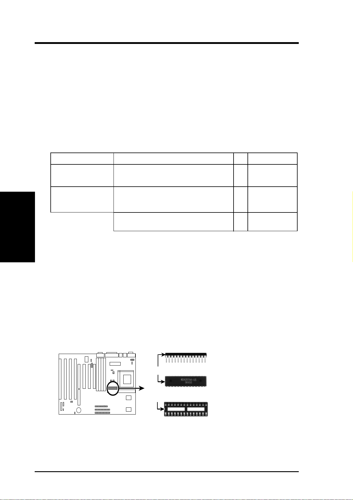
TAG SRAM Upgrade:
The purpose of this SRAM is described on page 9. You must use a standard 5Volt
SRAM chip that is 15ns or faster . See the illustration below for installation location
and orientation.
Insert one 16K8 or 32K8
SRAM chip as shown by
the Top view with the semicircle "Indention" on the
same side as the "Notch."
Indention
SRAM Chip Side
SRAM Chip Top
Notch
TAG SRAM Upgrade Socket
WARNING: If the cache module that you install already have an extended tag, do
not install another TAG SRAM into the TAG SRAM Upgrade Socket.
12 ASUS P/I-XP55T2P4 User’s Manual
III. INSTALLATION
DRAM Memory Installation Procedures:
1. The SIMM memory modules will only fit in one orientation as shown because
of a "Plastic Safety Tab" on one end of the SIMM sockets which requires the
"Notched End" of the SIMM memory modules.
1234
Bank 0 Bank 1
72 Pin SIMM DRAM Sockets & Module
Notched End
2. Press the memory module firmly into place starting from a 45 degree angle
making sure that all the contacts are aligned with the sockets.
3. With your finger tips, rock the memory module into a vertical position so that
it clicks into place.
72 Pin DRAM in SIMM Socket
Metal Clip
Plastic Safety Tab (This Side Only)
4. The plastic guides should go through the two "Mounting Holes" on the sides
and the "Metal Clips" should snap on the other side.
Mounting Hole
(DRAM Memory)
III. INSTALLATION
5. T o release the memory module, squeeze both "Metal Clips" outwards and rock
the module out of the "Metal Clips".
ASUS P/I-XP55T2P4 User’s Manual 13
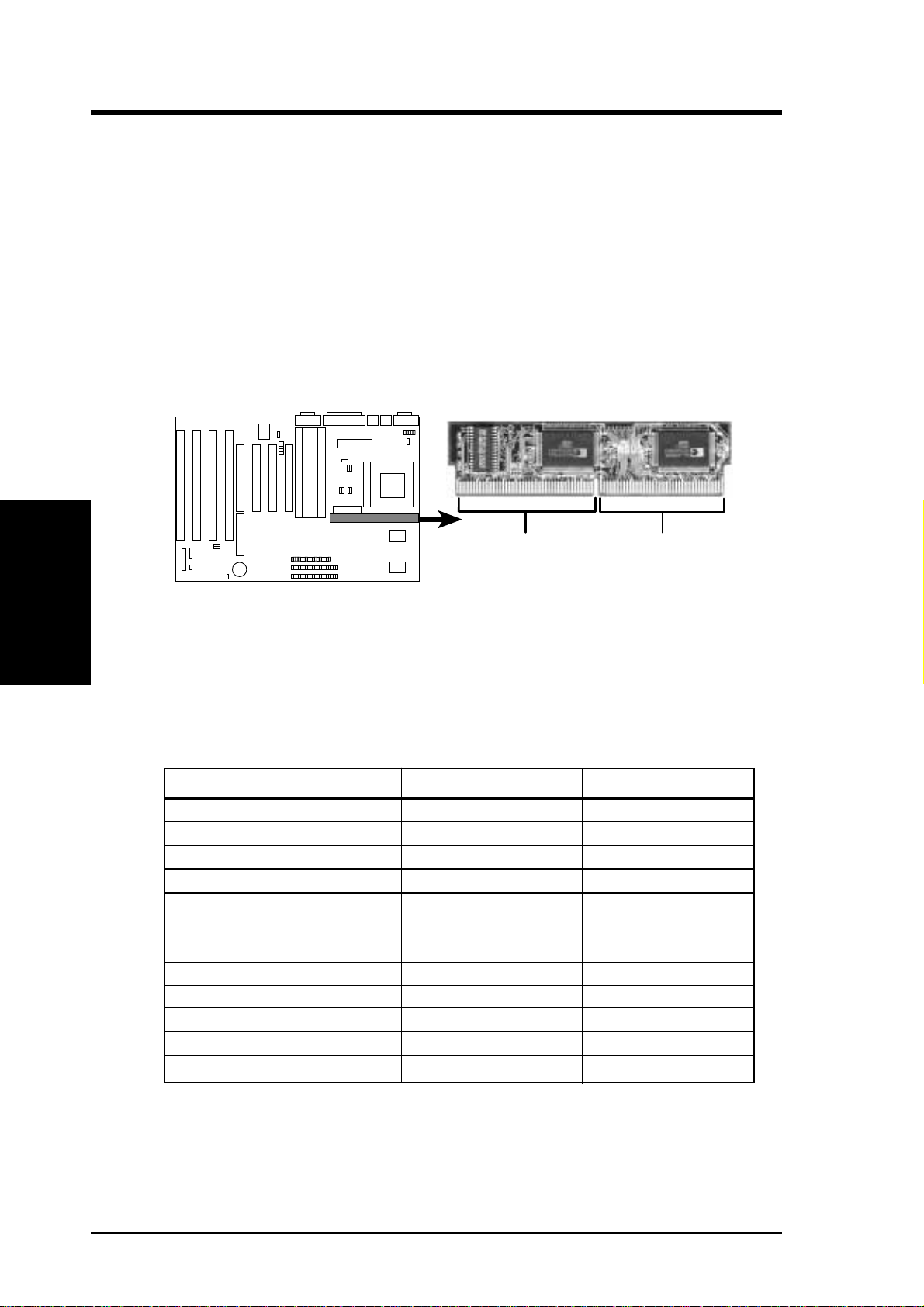
Static RAM (SRAM) for Level 2 (External) Cache
The motherboard you purchase may have either 0KB, 256KB, or 512KB onboard.
If you have both onboard cache chips (see "Map of Motherboard" for locations) and
a Cache Expansion Slot, then you have 256KB. If you only have onboard cache
chips, then you have 512KB. An "ASUS" or "COAST" cache module can be used
to upgrade the 256KB version to 512KB. If there is no onboard cache, you may
install a cache module of either 256KB or 512KB.
IMPORTANT: You must set jumper 1 "Total Level 2 Cache Size Setting" on
page 8 when changes are made to your cache size.
III. INSTALLATION
(SRAM Cache)
III. INSTALLATION
42 Pins 38 Pins
Pipelined Burst Cache Module
Insert the module as shown. Because the number of pins are different on either side
of the break, the module will only fit in the orientation as shown.
Compatible Cache Modules for this Motherboard
SIMM Cache Module 256KB Onboard 0KB Onboard
ASUS CM1 Rev 1.0 ---- ---ASUS CM1 Rev 1.3 ---- ---ASUS CM4 Rev 1.5 ---- ---ASUS CM1 Rev 1.6 Yes ---ASUS CM1 Rev 3.0* Yes Yes
COAST 1.1 ---- ---COAST 1.2 ---- ---COAST 1.3 ---- ---COAST 2.0 Yes Yes
COAST 2.1 Yes Yes
COAST 3.0 Yes Yes
COAST 3.1 Yes Yes
*NOTE: ASUS CMI Rev 3.0 has two TAG SRAM's to comply with COAST 3.0
specifications. This extra T AG SRAM will not conflict with the onboard T AG SRAM.
14 ASUS P/I-XP55T2P4 User’s Manual
 Loading...