

Page 1
MG3700A Vector Signal Generator
MX370x series software
MX3700xxA Waveform pattern
MX3701xxA IQproducer
Superior Expandability Supporting A Wide Variety Of Communication Systems
Page 2

MX370x series software
The MG3700A Vector Signal Generator (hereafter referred to as “MG3700A”) is a signal generator that integrates
a 160-MHz high-speed ARB baseband generator.With features that include a broadband vector modulation
bandwidth and large-capacity ARB memory, it supports digital modulation signals for a variety of communication
systems.The MG3700A provides optimal performance for generating signals for new wireless communications
in advancing broadband technology, as well as for major mobile telecommunication systems such as mobile
phones and wireless LANs.
Since the standard MG3700A comes equipped with an ARB generator,modulation signals can be output simply
by selecting a waveform pattern that conforms to each supported communication system.The following four
categories of waveform patterns are available for the MG3700A:
Standard waveform patterns
•
Waveform patterns generated by the optional waveform pattern option (Model: MX3700xxA)
•
Waveform patterns generated by the optional waveform generation software IQproducer (Model: MX3701xxA)
•
Waveform patterns converted from data generated by commonly-used signal generation software, so
•
as to be available for the MG3700A.
Each waveform category above contains multiple waveform pattern files in which parameters conforming to
each communication system are set in advance.The default waveform patterns are saved on the MG3700A hard
disk, allowing users to make free use of them. In addition, optional waveform patterns are also available.
The waveform generation software IQproducer is provided with the system to support various communication
methods. Parameter setting for the waveform data of a corresponding communication system can generate an
arbitrary waveform pattern file that can be used by MG3700A.
MG3700A can output signals by choosing a waveform pattern when the generated arbitrary waveform pattern
file is downloaded to MG3700A via LAN or a CompactFlash (CF) card.
Furthermore, an IQ sample file in ASCII format, generated by common EDA (Electronic Design Automation)
software such as MATLAB
arbitrarily generate a custom waveform pattern file.
®
, can be converted into a waveform pattern file for MG3700A.Thus, a user can
Selection guide
Waveform pattern IQproducer
Communication system Page MX370001A
W-CDMA 4 ✓✓
HSDPA 24 ✓✓
GSM 11 ✓
EDGE 11 ✓
CDMA2000 10 ✓
CDMA2000 1xEV-DO 8, 31 ✓ ✓
TD-SCDMA 18 ✓
PDC 13, 14, 28 ✓✓
PHS 12, 28 ✓✓
WLAN IEEE802.11a 15 ✓
WLAN IEEE802.11b 15 ✓
WLAN IEEE802.11g 15 ✓
RCR STD-39 21 ✓
ARIB STD-T61 21, 28 ✓✓
ARIB STD-T79 21, 28 ✓✓
ARIB STD-T86 21, 28 ✓✓
AWGN 16 ✓
CDMA2000®is a registered trademark of the Telecommunications Industry Association (TIA-USA).
Standard
TD-SCDMA
MX370002A
Public Radio
System 1xEV-DO
MX370101A MX370102A
HSDPA TDMA
MX370103A
CDMA2000
®
2
Page 3
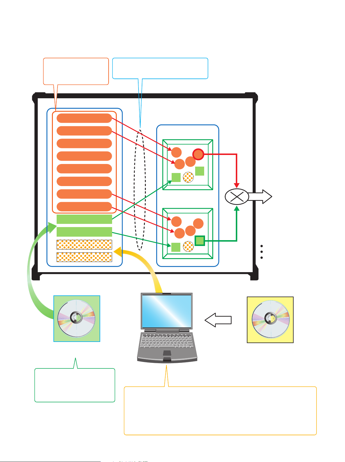
Memory A
Memory B
HDD 40GB
Output signal
Waveform patterns can be
selected from both ARB
memories A and B, and
one of the following
methods can be selected
for output:
A only
B only
Addition of A and B
MX370101A
HSDPA IQproducer
MX370102A
TDMA IQproducer
MX370103A
CDMA2000 1xEV-DO IQproducer
IQproducer is PC application software.
The waveform patterns available with the MG3700A can be generated by editing
the parameters for the modulation signals according to the appropriate
communication systems.
The generated waveform patterns are saved in the MG3700A once and then
loaded to the waveform memory for use.
Optional waveform patterns are
saved in the MG3700A once
and then loaded to the
waveform memory for use.
MX370001A TD-SCDMA
MX370002A Public radio system
From IQproducer
From IQproducer
TD-SCDMA
Public radio system
AWGN
WLAN
PHS
PDC
CDMA2000 1xEV-DO
CDMA2000
GSM/EDGE
W-CDMA
ARB memory
1 GB = 256 M samples (Std)
2 GB = 512 M samples (Opt)
Waveform patterns are transferred from
the HDD to ARB memory.
MG3700A Vector Signal Generator
The standard waveform
patterns are saved on the
MG3700A hard disk.
Download
Install
Download
3
Page 4
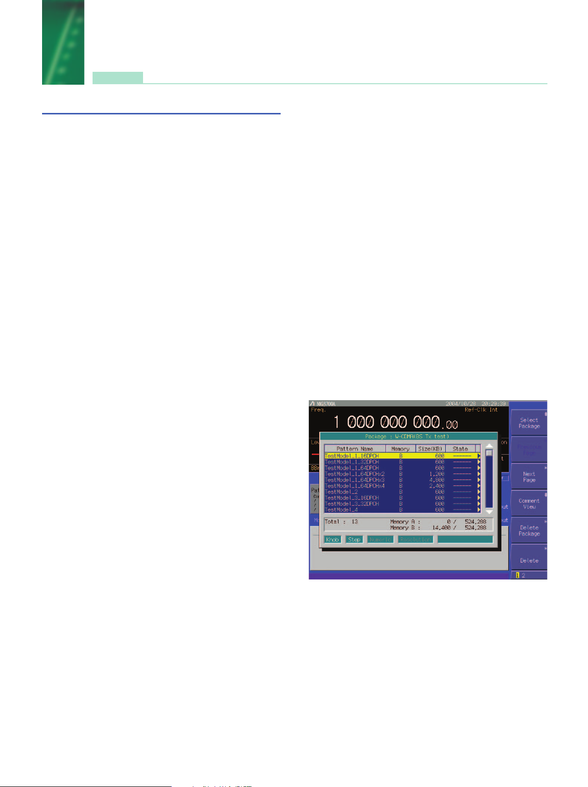
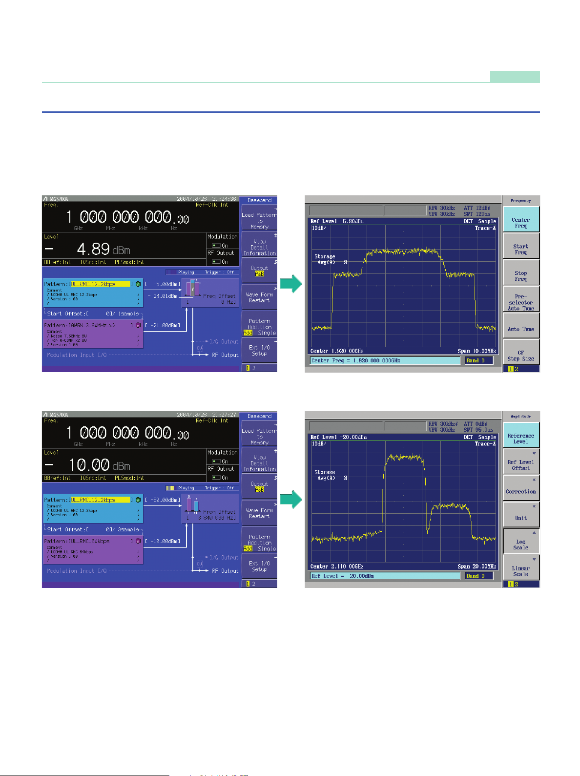
W-CDMA waveform pattern
Standard
■W-CDMA waveform pattern:
The W-CDMA waveform patterns listed below are provided on
the MG3700A internal hard disk as standard (see the next page
for details):
For evaluating transmitter device of BS
•
(TS 25.141 Test Model 1 to 4)
TestModel_1_16DPCH
TestModel_1_32DPCH
TestModel_1_64DPCH
TestModel_1_64x2_10M
TestModel_1_64x2_15M
TestModel_2
TestModel_3_16DPCH
TestModel_3_32DPCH
TestModel_4
TestModel_5_2HSPDSCH
TestModel_5_4HSPDSCH
TestModel_5_8HSPDSCH
TestModel_1_64DPCHx2
TestModel_1_64DPCHx3
TestModel_1_64DPCHx4
For testing receivers and performance of BS and
•
evaluating transmitter devices of UE
(TS 25.101/ 25.104 UL RMC 12.2 to 384 kbps)
UL_RMC_12_2kbps
UL_RMC_12_2kbps_ACS
UL_RMC_64kbps
UL_RMC_144kbps
UL_RMC_384kbps
UL_AMR_TFCS1
UL_AMR_TFCS2
UL_AMR_TFCS3
UL_ISDN
UL_64kbps_Packet
UL_Interfere
UL_RMC_12_2kbps_TX
For testing receivers and performance of UE
•
(TS 25.101 DL RMC 12.2 to 384 kbps)
DL_RMC_12_2kbps_RX
DL_RMC_12_2kbps
DL_RMC_12_2kbps_MIL
DL_RMC_12_2kbps_ACS
DL_RMC_64kbps
DL_RMC_144kbps
DL_RMC_384kbps
DL_AMR_TFCS1
DL_AMR_TFCS2
DL_AMR_TFCS3
DL_ISDN
DL_384kbps_Packet
DL_Interfere
P_CCPCH
DL_CPICH
Uplink/downlink W-CDMA modulation signals conforming to the
3GPP (FDD) standards can be output simply by selecting a
waveform pattern loaded from the MG3700A internal hard disk
to the large-capacity ARB memory, without setting any complex
3GPP-compliant parameters.
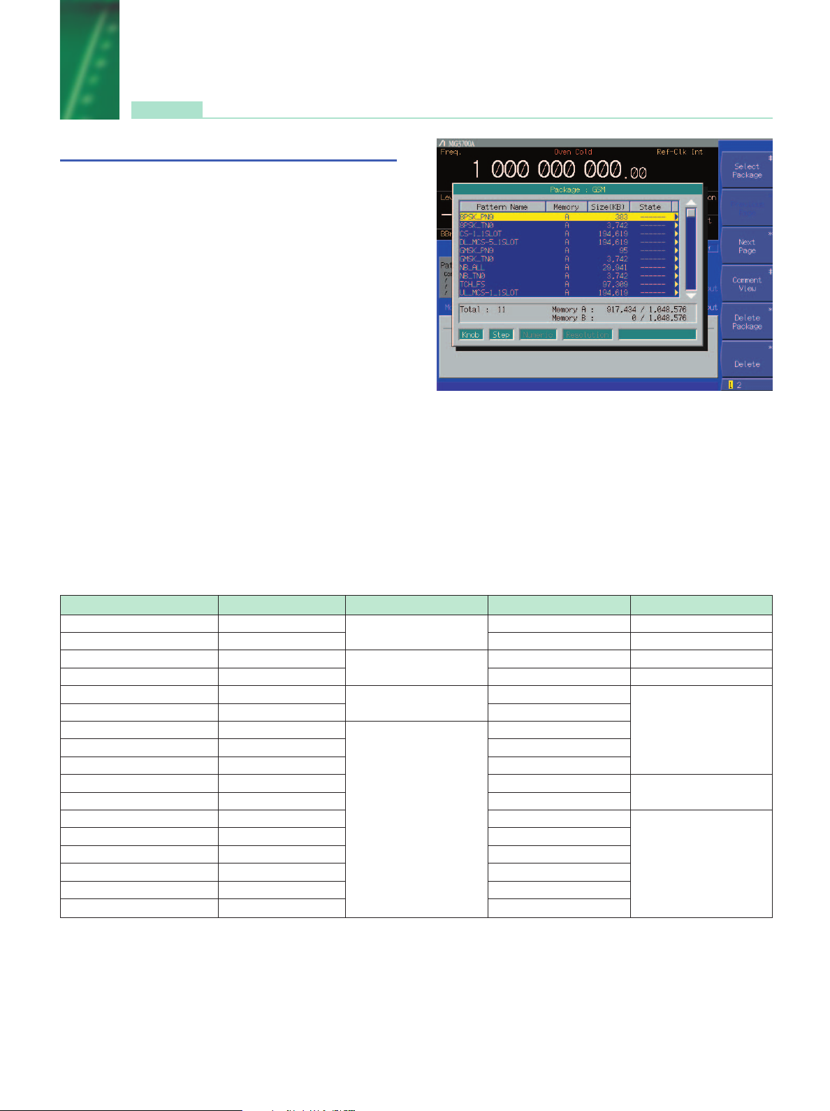
Example of selecting a waveform pattern
4
Page 5

W-CDMA waveform pattern
Standard
W-CDMA waveform pattern list
•
Waveform pattern UL/DL Channel 3GPP (Release1999) Evaluation
UL_RMC_12_2kbps DPCCH, DPDCH
UL_RMC_12_2kbps_ACS DPCCH, DPDCH
UL_RMC_64kbps
UL_RMC_144kbps
UL_RMC_384kbps
UL_AMR_TFCS1 DPCCH, DPDCH BS RX test
UL_AMR_TFCS2 DPCCH, DPDCH
UL_AMR_TFCS3 DPCCH, DPDCH TS25.944 4.1.2
UL_ISDN
UL_64kbps_Packet DPCCH, DPDCH
UL_Interfere DPCCH, DPDCH TS25.141 I
UL_RMC_12_2kbps_TX DPCCH, DPDCH TS25.101 A.2.1
P_CCPCH P_CCPCH TS25.944 4.1.1
DL_RMC_12_2kbps_RX
DL_RMC_12_2kbps_ACS P-CPICH, P-CCPCH, SCH, PICH, DPCH
DL_RMC_12_2kbps
DL_RMC_12_2kbps_MIL
DL_RMC_64kbps
DL_RMC_144kbps
DL_RMC_384kbps
DL_AMR_TFCS1
DL_AMR_TFCS2
DL_AMR_TFCS3
DL_ISDN
DL_384kbps_Packet
DL_Interfere P-CPICH, P-CCPCH, SCH, PICH, DPCH, OCNS TS25.101 C.4
DL_CPICH P-CPICH —
TestModel_1_16DPCH
TestModel_1_32DPCH
TestModel_1_64DPCH
TestModel_2
TestModel_3_16DPCH
TestModel_3_32DPCH
TestModel_4 P-CCPCH, SCH
TestModel_5_2HSPSDCH
TestModel_5_4HSPSDCH
TestModel_5_8HSPSDCH
TestModel_1_64DPCHx2 ∗4
TestModel_1_64DPCHx3 ∗4
TestModel_1_64DPCHx4 ∗4
TestModel_1_64x2_10M
TestModel_1_64x2_15M
1: UL_ISDN can be combined with AWGN that is a standard waveform pattern only when Option 021/121 ARB Memory Upgrade 512M samples is installed.
∗
2: P-CCPCH is not included in the waveform patterns such as RMC for UE RX test. They must be used in combination with P-CCPCH waveform patterns.
∗
3: 12-bit SFN is added to the head of the BCH transport block.
∗
4: x2, x3, and x4 represent the number of multi-carrier signals 2, 3, and 4, respectively.
∗
∗1
∗1
∗1
UL
∗1
2
∗
∗2
∗2
∗2
∗2
∗2
∗2
∗2
∗2
∗2
∗2
DL
DPCCH, DPDCH TS25.104 A.3
DPCCH, DPDCH TS25.104 A.4
DPCCH, DPDCH TS25.104 A.5
DPCCH, DPDCH
P-CPICH, SCH, PICH, DPCH
P-CCPCH, SCH, PICH, DPCH, OCNS
P-CCPCH, SCH, PICH, DPCH, OCNS
P-CCPCH, SCH, PICH, DPCH, OCNS
P-CCPCH, SCH, PICH, DPCH, OCNS
P-CCPCH, SCH, PICH, DPCH, OCNS
P-CCPCH, SCH, PICH, DPCH, OCNS
P-CCPCH, SCH, PICH, DPCH, OCNS
P-CCPCH, SCH, PICH, DPCH, OCNS
P-CCPCH, SCH, PICH, DPCH, OCNS
P-CCPCH, SCH, PICH, DPCH, OCNS
P-CPICH, P-CCPCH, SCH, PICH, S-CCPCH, 16 DPCH
P-CPICH, P-CCPCH, SCH, PICH, S-CCPCH, 32 DPCH
P-CPICH, P-CCPCH, SCH, PICH, S-CCPCH, 64 DPCH
P-CPICH, P-CCPCH, SCH, PICH, S-CCPCH, DPCH
P-CPICH, P-CCPCH, SCH, PICH, S-CCPCH, 16 DPCH
P-CPICH, P-CCPCH, SCH, PICH, S-CCPCH, 32 DPCH
P-CPICH, P-CCPCH, SCH, PICH, S-CCPCH,
6DPCH, HS-SCCH, 2HS-PDSCH BS TX
P-CPICH, P-CCPCH, SCH, PICH, S-CCPCH,
14DPCH, HS-SCCH, 4HS-PDSCH
P-CPICH, P-CCPCH, SCH, PICH, S-CCPCH,
30DPCH, HS-SCCH, 8HS-PDSCH
P-CPICH, P-CCPCH, SCH, PICH, S-CCPCH, 64 DPCH
P-CPICH, P-CCPCH, SCH, PICH, S-CCPCH, 64 DPCH
P-CPICH, P-CCPCH, SCH, PICH, S-CCPCH, 64 DPCH
P-CPICH, P-CCPCH, SCH, PICH, S-CCPCH, 64 DPCH
P-CPICH, P-CCPCH, SCH, PICH, S-CCPCH, 64 DPCH
TS25.104 A.2
TS25.101 A.3.1
TS25.101 C.3.1
TS25.101 A.3.1
TS25.101 C.3.2
TS25.944 4.1.1.3
TS25.101 C.3.2
TS25.141 6.1.1
∗3
UE TX device test
UE RX test
device test
5
Page 6
W-CDMA waveform pattern
Standard
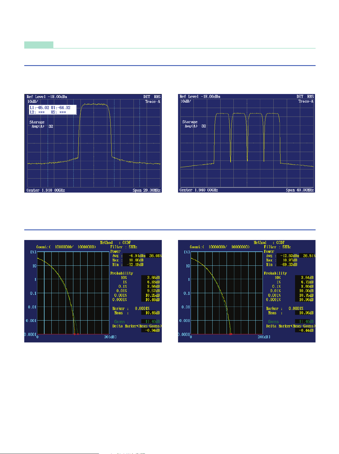
■ACPR:
The adjacent channel leakage power ratio of a Vector Signal Generator is an important factor in device distortion testing and receiver
interference testing.
W-CDMA ACPR (Test Model 1, 64 DPCH, 1carrier)
Waveform pattern [Test_Model_1_64DPCH]
■CCDF:
CCDF (Test Model 1, 64 DPCH, 1carrier)
Waveform pattern [Test_Model_1_64DPCH]
W-CDMA ACPR (Test Model 1, 64 DPCH, 4carrier)
Waveform pattern [Test_Model_1_64DPCH x4]
CCDF (Test Model 1, 64 DPCH, 4carrier)
Waveform pattern [Test_Model_1_64DPCH x4]
6
Page 7
W-CDMA waveform pattern
Standard
■AWGN (Additive White Gaussian Noise) Supports Dynamic Range Test
When performing the receiver dynamic range test specified by 3GPP, AWGN with a W-CDMA modulation signal is required.
Either of the AWGN waveform patterns AWGN_3_84MHz_x2 or AWGN_3_84MHz_x1_5, which are stored on the MG3700A internal
hard disk, can be used for an AWGN signal.
Since a single MG3700A can add a W-CDMA uplink modulation signal and AWGN signal internally and output them as a combined
signal, it is useful for a simple dynamic range test for base station receivers.
Wanted signal + AWGN screen Output waveform screen of Wanted signal + AWGN
Wanted signal + Interfering signal screen Output waveform screen of Wanted signal + Interfering signal
7
Page 8
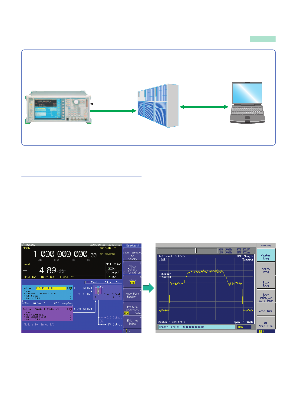
CDMA2000 1xEV-DO waveform pattern
MG3700A Vector Signal Generator
AT control, PER calculation
AT
Modulation signal
(Downlink)
Standard
■CDMA2000 1xEV-DO waveform pattern:
The CDMA2000 1xEV-DO waveform patterns listed on the right
are provided on the MG3700A internal hard disk.
The signals for testing the receiver and transmitter of the
CDMA2000 1xEV-DO access network (base station) and
access terminal (mobile station), which are specified in 3GPP2,
can be output by selecting one of these CDMA2000 1xEV-DO
waveform patterns. Thirteen forward and ten reverse data rate
waveform patterns are available.
When multi-carrier signals, mixed signals of idle and active,
and/or multi-user signals are required, parameter setting and
waveform pattern generation are available using the optional
MX370103A CDMA2000 1xEV-DO IQproducer.
Example of selecting a waveform pattern
Access terminal (AT) receiver test
•
CDMA2000 1xEV-DO forward
Base band filter: IS-95SPEC +EQ
Data: PN15fix∗(excluding FWD-Idle)
FWD_38_4kbps_16slot
FWD_76_8kbps_8slot
FWD_153_6kbps_4slot
FWD_307_2kbps_2slot
FWD_614_4kbps_1slot
FWD_307_2kbps_4slot
FWD_614_4kbps_2slot
FWD_1228_8kbps_1slot
FWD_921_6kbps_2slot
FWD_1843_2kbps_1slot
FWD_1228_8kbps_2slot
FWD_2457_6kbps_1slot
FWD_Idle
Access network (AN) receiver test
•
CDMA2000 1xEV-DO Reverse
Base band filter: IS-95SPEC
Data: PN9fix
RVS_9_6kbps_RX
RVS_19_2kbps_RX
RVS_38_4kbps_RX
RVS_76_8kbps_RX
RVS_153_6kbps_RX
RVS_9_6kbps_TX
RVS_19_2kbps_TX
RVS_38_4kbps_TX
RVS_76_8kbps_RT
RVS_153_6kbps_RT
This is a PN sequence delimited for each packet. Therefore, the PN
∗
sequence is discontinuous between the end data of a packet and the
start data of the next packet.
∗
Access terminal (AT) receiver test
•
3GPP2 C.S0033 standard receiver tests (PER: Packet Error Rate) can be performed by selecting a forward signal pattern
required for testing the AT. No protocol is supported for the access network simulator. In addition, all the transmission channels
are traffic, and all the other channels (e.g., Sync) are unsupported; it is necessary to calculate the PER by controlling the AT
using an external controller.
8
Page 9
CDMA2000 1xEV-DO waveform pattern
MG3700A Vector Signal Generator
Trigger∗, Clock
∗
Modulation signal (Uplink)
AN control, PER calculation
AN
Standard
Access network (AN) receiver test
•
GPP2 C.S0032 standard receiver tests (PER: Packet Error Rate) can be performed by selecting a reverse signal pattern required
for testing the AN. Since access terminal simulator protocols are not supported, an external controller must be used to control the
AN and calculate PER.
∗ Trigger: Timing for synchronizing the start of frame (frame trigger)
∗ Clock: Clock for synchronizing the chip rate 1.2288 Mcps (11 x 1.2288 MHz or 5MHz/10 MHz)
■AWGN Supports Dynamic Range Test
(AWGN: Additive White Gaussian Noise)
When performing the receiver dynamic range test specified by
3GPP2, a 1xEV-DO modulation signal with AWGN is required.
Either of the AWGN waveform patterns AWGN_1.23MHz_x2 or
AWGN_1.23MHz_x1_5, which are stored on the MG3700A
internal hard disk, can be used for an AWGN signal.
Since a single MG3700A can add a CDMA2000 uplink
modulation signal and an AWGN signal internally and output
them as a combined signal, it is useful for a simple dynamic
range test for an AN receiver.
Wanted signal + AWGN screen Output waveform screen of wanted signal + AWGN
9
Page 10
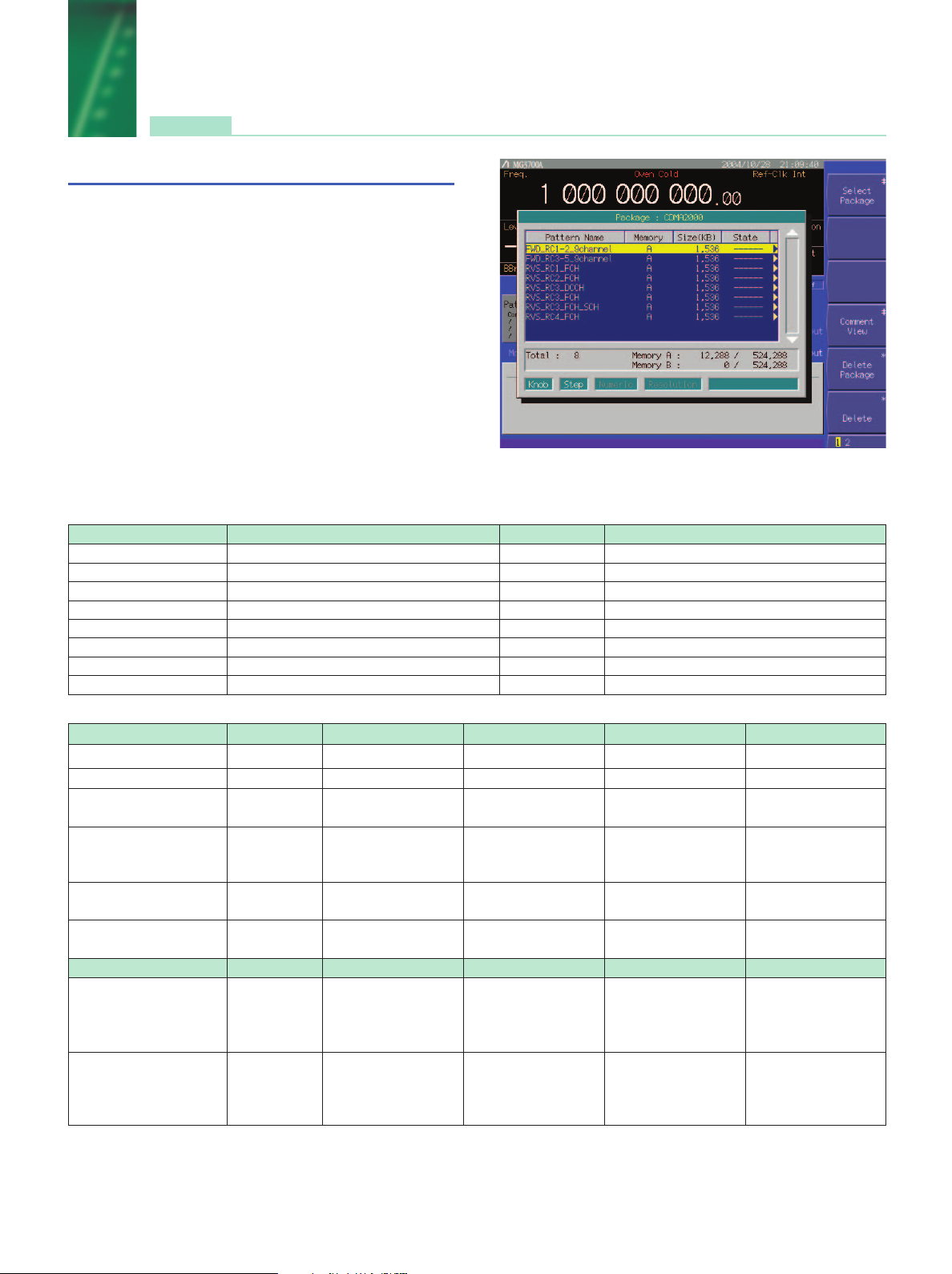
CDMA2000 waveform pattern
Standard
■CDMA2000 waveform pattern:
The CDMA2000 waveform patterns listed in the table below are
provided on the MG3700A internal hard disk.
CDMA2000 modulation signals specified in 3GPP2 C.S0002-0-2
can be output by selecting one of these CDMA2000 waveform
patterns.
Since reverse channel signals are output by channel coding
(convolutional coding, etc.) 4-frame length PN9 fix
useful for Frame Error Rate (FER) measurement
station, as well as device evaluation.
1: The data length is not an integer multiple of the PN sequence
∗
length (511 bits for PN9), and the PN sequence becomes
discontinuous at the end.
2: This is the case where the timing signal and 1.2288 Mcps x 11
∗
clock signal (or 5 or 10 MHz reference clock) can be input from the
test target base station to the MG3700A in order to provide
synchronization of the frame start point and chip clock.
Waveform pattern System Frame coding Symbol data
RVS_RC1_FCH CDMA2000 1xRTT RC1 Reverse Coded FCH 9.6 kbps
RVS_RC2_FCH CDMA2000 1xRTT RC2 Reverse Coded FCH 14.4 kbps
RVS_RC3_FCH CDMA2000 1xRTT RC3 Reverse Coded PICH, FCH 9.6 kbps
RVS_RC3_FCH/SCH CDMA2000 1xRTT RC3 Reverse Coded PICH, FCH 9.6 kbps, SCH 9.6 kbps
RVS_RC3_DCCH CDMA2000 1xRTT RC3 Reverse Coded PICH, DCCH 9.6 kbps
RVS_RC4_FCH CDMA2000 1xRTT RC4 Reverse Coded PICH, FCH 14.4 kbps
FWD_RC1-2_9channel CDMA2000 1xRTT RC1, RC2 Forward spreading only PICH, SyncCH, PagingCH, FCH19.2 ksps x 6
FWD_RC3-5_9channel CDMA2000 1xRTT RC3, RC4, RC5 Forward spreading only PICH, SyncCH, PagingCH, FCH 38.4 ksps x 6
1
∗
data, it is
2
∗
of the base
Example of selecting waveform pattern
Waveform pattern Walsh Code Code Power Data Rate Data
RVS_RC1_FCH R-FCH 9.6 kbps PN9fix
RVS_RC2_FCH R-FCH 14.4 kbps PN9fix
RVS_RC3_FCH
RVS_RC3_FCH/SCH R-FCH 4 –3.8412 dB 9.6 kbps PN9fix
RVS_RC3_DCCH
RVS_RC4_FCH
Waveform pattern Walsh Code Code Power Symbol Rate Symbol Data
FWD_RC1-2_9channel
FWD_RC3-5_9channel
R-PICH (Reverse Pilot Channel),
R-FCH (Reverse Fundamental Channel)
R-SCH (Reverse Supplemental Channel)
R-DCCH (Reverse Dedicated Control Channel)
R-PICH 0 –5.278 dB N/A All "0"
R-FCH 4 –1.528 dB 9.6 kbps PN9fix
R-PICH 0 –7.5912 dB N/A All"0"
R-SCH 2 –3.8412 dB 9.6 kbps PN9fix
R-PICH 0 –5.278 dB N/A All"0"
R-DCCH 8 –1.528 dB 9.6 kbps PN9fix
R-PICH 0 –5.278 dB N/A All"0"
R-FCH 4 –1.528 dB 14.4 kbps PN9fix
F-PICH 0 –7.0 dB N/A All"0"
F-SyncCH 32 –13.3 dB 4.8 kbps PN9fix
PagingCH 1 –7.3 dB 19.2 kbps PN9fix
F-FCH x6 8-13 –10.3 dB 19.2 kbps PN9fix
F-PICH 0 –7.0 dB N/A All"0"
F-SyncCH 32 –13.3 dB 4.8 kbps PN9fix
PagingCH 1 –7.3 dB 19.2 kbps PN9fix
F-FCH x6 8-13 –10.3 dB 38.4 kbps PN9fix
F-PICH (Forward Pilot Channel),
F-SyncCH (Forward Sync Channel),
PagingCH (Paging Channel),
F-FCH (Forward Fundamental Channel)
∗
∗
∗
∗
∗
∗
∗
∗
∗
∗
∗
∗
∗
10
Page 11
GSM/EDGE waveform pattern
Standard
■GSM/EDGE waveform pattern:
The GSM/EDGE waveform patterns listed in the table below
are provided on the MG3700A internal hard disk.
The signals suitable for testing receivers and for managing
device evaluation in a GSM/EDGE system can be output by
selecting one of these GSM/EDGE waveform patterns.
GMSK_PN9, 8PSK_PN9
•
PN9 data is inserted into the entire area of the slots, except the
guard. The PN9 data in each slot are continuous.
GMSK_TN0, 8PSK_TN0
•
PN9 data is inserted into the entire area of the slots, except the
guard. The PN9 data in each slot are continuous.
NB_TN0, NB_ALL
•
PN9 data is inserted into the normal burst encrypted bit area.
The PN9 data in the slots are continuous.
TCH_FS
•
Supports the Speech channel at the full rate (TCH/FS) specified
in Section 3.1 of 3GPP TS05.03.
CS-1_1 (4)_SLOT (_4SLOT )
•
Supports the packet data block type 1 (CS-4) and 4 (CS-1)
specified in Section 5.1 of 3GPP TS05.03.
DL (UL)_MCS-1 (5, 9)_1SLOT (_4SLOT)
•
Supports the packet data block types 5(MCS-1), 9(MCS-5), and
13 (MCS-9) specified in Section 5.1 of 3GPP TS05.03.
Example of selecting waveform pattern
Waveform pattern Uplink / Downlink Data Output slot Communications
GMSK_PN9 Uplink / Downlink
8PSK_PN9 Uplink / Downlink
GMSK_TN0 Uplink / Downlink TN0
8PSK_TN0 Uplink / Downlink TN0
NB_TN0 Uplink / Downlink TN0
NB_ALL Uplink / Downlink All slot
TCH_FS Uplink / Downlink TN0 GSM
CS-1_1SLOT Uplink / Downlink TN0
CS-4_1SLOT Uplink / Downlink TN0
DL_MCS-1_1SLOT Uplink / Downlink TN0
UL_MCS-1_1SLOT Uplink / Downlink TN0
DL_MCS-5_1SLOT Uplink / Downlink TN0
UL_MCS-5_1SLOT Uplink / Downlink TN0
DL_MCS-9_1SLOT Uplink / Downlink TN0
UL_MCS-9_1SLOT Uplink / Downlink TN0
DL_MCS-9_4SLOT Uplink / Downlink TN0, 1, 2, 3
UL_MCS-9_4SLOT Uplink / Downlink TN0, 1, 2, 3
1: PN9 data is inserted into the entire area that does not have the slot format.
∗
2: PN9 data is inserted into the entire area of the slots, except the guard.
∗
3: PN9 is inserted into the normal burst encrypted bit area.
∗
4: The bit string channel-coded for PN9 data is inserted into the normal burst encrypted bit area.
∗
PN9
PN9
PN9
PN9
1
∗
2
∗
3
∗
4
∗
––
––
–
–
GPRS
EDGE
11
Page 12

PHS waveform pattern
•
PS receiver test
MG3700A Vector Signal Generator
Modulation signal (Downlink)
Data, Clock
BER analyzer is built in.
PS
CS
•
PS receiver test
MG3700A Vector Signal Generator
BER analyzer is built in.
Modulation signal (Uplink)
Data, Clock
Trigger
∗
Standard
■PHS waveform pattern:
The PHS waveform patterns listed in the table below are
provided on the MG3700A internal hard disk.
The signals for testing CS (base station) and PS (mobile station)
receivers, which are specified in RCR STD-28, can be output
by selecting one of these PHS waveform patterns, without
setting any complex RCR STD-28 parameters.
When a signal that has parameters different from those of the
provided waveform patterns are required, parameter setting
and waveform pattern generation are available using the
optional MX370102A TDMA IQproducer.
Waveform pattern Uplink / Downlink Scramble Output slot
PI_4_DQPSK_PN9
PI_4_DQPSK_PN15
PI_4_DQPSK_ALL0
DL_TCH_Slot_1 Uplink / Downlink OFF
UL_TCH_Slot_1 Uplink / Downlink OFF
—
—
—
OFF No frame
OFF No frame
OFF No frame
Example of selecting waveform pattern
Slot1: TCH
Slot 2 to 4: off
Slot1: TCH
Slot 2 to 4: off
Trigger: Timing for synchronizing frames (frame trigger)
∗
12
Page 13

PDC waveform pattern
Standard
■PDC waveform pattern:
The waveform patterns for the wanted signals/interfering signals
required to execute transmission/reception tests as specified in
ARIB STD-27 are provided on the MG3700A internal hard disk.
Modulation signals conforming to the standard can be output
without any options (Note: Check the parameters listed on the
next page in advance).
The waveform pattern to output uplink/downlink Slot 0 data
only and the unframed waveform pattern for interfering signals
are provided for full rate and half rate, respectively.
When a signal is required that has parameters different from
those of the provided waveform patterns, parameter setting and
waveform pattern generation are available using the optional
MX370102A TDMA IQproducer.
Example of selecting waveform pattern
Waveform pattern Uplink / Downlink Half rate / Fill rate Output slot Evaluation
PI_4_DQPSK_PN9
PI_4_DQPSK_PN15
DL_Full_Rate_Slot0 Uplink / Downlink Full rate Slot 0 only
DL_Half_Rate_Slot0 Uplink / Downlink Half rate Slot 0 only Wanted signal for
UL_Full_Rate_Slot0 Uplink / Downlink Full rate Slot 0 only receiver test
UL_Half_Rate_Slot0 Uplink / Downlink Half rate Slot 0 only
——
——
No frame TX device test
No frame Interfering signal
13
Page 14

PDC Packet waveform pattern
•
Mobile station test
MG3700A Vector Signal Generator
Modulation signal (Downlink)
Data, Clock
BER analyzer is built in.
Mobile device
Base station
•
Base station test
MG3700A Vector Signal Generator
BER analyzer is built in.
Modulation signal (Uplink)
Data, Clock
Trigger
∗
Standard
■PDC Packet waveform pattern:
The four types of waveform patterns listed in the table below
are provided on the MG3700A internal hard disk.
The signals for testing base station and mobile station
receivers for UPCH communications, which are specified in
RCR STD-27, can be output by selecting one of these
waveform patterns, without setting any complex RCR STD-27
parameters. Also, the Downlink3 data rate UPHC pattern and
Uplink1 UPHC pattern can be switched.
When a signal is required that has parameters different from
those of the provided waveform patterns, parameter setting and
waveform pattern generation are available using the optional
MX370102A TDMA IQproducer.
Waveform pattern Uplink / Downlink Output slot
Slot 0 = UPCH
DL_Packet_Slot_0 Uplink / Downlink Slot 1 = IDLE (all "1")
Slot 2 = IDLE (all "1")
Slot 0 = UPCH
DL_Packet_Slot_01 Uplink / Downlink Slot 1 = UPCH
Slot 2 = IDLE (all "1")
Slot 0 = UPCH
DL_Packet_Slot_all Uplink / Downlink Slot 1 = UPCH
Slot 2 = UPCH
Slot 0 = UPCH
UL_Packet_Slot_0 Uplink / Downlink Slot 1 = Transmit off
Slot 2 = Transmit off
Example of selecting waveform pattern
Trigger: Timing for synchronizing sub frames (frame trigger)
∗
14
Page 15

WLAN waveform pattern
Standard
■WLAN waveform pattern:
The WLAN (IEEE802.11a/b/g) waveform patterns listed in the
table below are provided on the MG3700A internal hard disk.
The signals for testing the receiver/transmitter of a terminal or
module can be output by selecting one of these WLAN
waveform patterns.
Example of selecting waveform pattern
IEEE_802.11a waveform pattern list
•
Waveform pattern
11a_OFDM_6Mbps 6 BPSK 1/2 1 48 24
11a_OFDM_9Mbps 9 BPSK 3/4 1 48 36
11a_OFDM_12Mbps 12 QPSK 1/2 2 96 48
11a_OFDM_18Mbps 18 QPSK 3/4 2 96 72
11a_OFDM_24Mbps 24 16-QAM 1/2 4 192 96
11a_OFDM_36Mbps 36 16-QAM 3/4 4 192 144
11a_OFDM_48Mbps 48 64-QAM 2/3 6 288 192
11a_OFDM_54Mbps 54 64-QAM 3/4 6 288 216
Data rate
(Mbits/s) sub-carrier OFDM symbol OFDM symbol
Modulation Coding rate
Coding bits per Coding bits per Data bits per
IEEE_802.11b waveform pattern list
•
Waveform pattern Spreading, Coding Modulation
11b_DSSS_1Mbps DSSS, 11 chip Barker Code DBPSK
11b_DSSS_2Mbps DSSS, 11 chip Barker Code DQPSK
11b_CCK_5_5Mbps CCK DQPSK
11b_CCK_11Mbps CCK DQPSK
IEEE_802.11g waveform pattern list
•
Waveform pattern
11g_DSSS_OFDM_6Mbps 6 BPSK 1/2 1 48 24
11g_DSSS_OFDM_9Mbps 9 BPSK 3/4 1 48 36
11g_DSSS_OFDM_12Mbps 12 QPSK 1/2 2 96 48
11g_DSSS_OFDM_18Mbps 18 QPSK 3/4 2 96 72
11g_DSSS_OFDM_24Mbps 24 16-QAM 1/2 4 192 96
11g_DSSS_OFDM_36Mbps 36 16-QAM 3/4 4 192 144
11g_DSSS_OFDM_48Mbps 48 64-QAM 2/3 6 288 192
11g_DSSS_OFDM_54Mbps 54 64-QAM 3/4 6 288 216
Data rate
(Mbits/s) sub-carrier OFDM symbol OFDM symbol
Modulation Coding rate
Coding bits per Coding bits per Data bits per
15
Page 16

AWGN waveform pattern
AWGNWGN
AWGN
AWGN band width
System band width
Wanted signal
In-band
AWGN
power
Standard
■AWGN waveform pattern:
The Additive White Gaussian Noise (AWGN) waveform patterns listed in the table below are provided on the MG3700A
internal hard disk.
The signals for testing the receiver/transmitter of a terminal or
module can be output by selecting one of these AWGN
waveform patterns.
Example of selecting a waveform pattern
Waveform pattern
AWGN_3_84MHz_x2 >12 dB 7.68 3.01
AWGN_3_84MHz_x1_5 >12 dB 5.76 1.76
AWGN_1.23MHz_x2 >12 dB 2.46 3.01 CDMA2000 or CDMA2000 1xEV-DO to
AWGN_1.23MHz_x1_5 >12 dB 3.69 1.76 CDMA2000 or CDMA2000 1xEV-DO to
In-band power conversion ratio is the ratio of the system bandwidth of each communication system to the total power of the MG3700A output measured with a
∗
power meter or another equivalent device.
MAX peak/RMS 3dB bandwidth In-band power
ratio (MHz) conversion ratio (dB)
∗
Added with the W-CDMA UL signal to
perform a dynamic range test.
Added with the W-CDMA UL signal to
perform a dynamic range test.
Added with the reverse signals of
perform a dynamic range test.
Added with the reverse signals of
perform a dynamic range test.
Evaluation
In-band AWGN power
16
Page 17

AWGN waveform pattern
Standard
■With the waveform combine function, a single MG3700A outputs a signal that is the addition (such
as modulation signal + AWGN) of the wanted signal and interfering signal:
The MG3700A has ARB memory that consists of two memory areas, each allowing one waveform pattern to be set. The addition of
the signals from the two memories, as well as the signal for either one, can be output.
For example, if a wanted signal (W-CDMA, CDMA2000) waveform pattern is selected for one memory and an interfering signal
(AWGN) waveform pattern for the other, a signal that is the addition of the wanted signal and interfering signal (AWGN) shown in the
upper figures below can be output with a single MG3700A.
Also, if a modulation signal is selected as the interfering signal, the addition of the wanted signal and interfering signal (modulation
signal) shown in the lower figures below can also be output with a single MG3700A.
Furthermore, the accuracy of the level ratio is superior since the S/N adjustment and calculation are performed by digital processing.
Wanted signal + AWGN screen
Wanted signal + interfering signal screen
Output waveform screen of wanted signal + AWGN
Output waveform screen of wanted signal + interfering signal
17
Page 18

MX370001A TD-SCDMA waveform pattern
MG3700A Vector Signal Generator
LAN
or
Compact Flash
PC
MX370001A
Optional
■TD-SCDMA waveform pattern:
The signals corresponding to the 3GPP 1.28Mcps TDD options
can be output by installing the MX370001A TD-SCDMA
waveform pattern on the MG3700A.
For evaluating transmitter of BS
•
(TS 25.141 Test Model 1 to 4)
BS_DL RMC 1Code
BS_DL RMC 1Code+P-CCPCH
BS_DL RMC 8Code
BS_DL RMC 10Code
For evaluating receiver of BS
•
BS_UL RMC 12.2k(Single)
BS_UL RMC 12.2k+OCNS
BS_UL RMC 64k+OCNS
BS_UL RMC 144k+OCNS
BS_UL RMC 384
For evaluating receiver of UE
•
UE_DL RMC 12.2k
UE_DL RMC 12.2k+OCNS
UE_DL RMC 64k+OCNS
UE_DL RMC 144k+OCNS
UE_DL RMC 384
■Simple operation and high speed signal
pattern change:
Typical waveforms specified in 3GPP, such as the reference
management channel, can be output simply by selecting the
waveform pattern loaded from the MG3700A internal hard disk
to the large-capacity ARB memory, without setting any complex
TD-SCDMA parameters.
Waveform patterns for evaluating BS transmitters
•
Target of test
Test signal BS-DL RMC
Waveform pattern rmc_1 code_bs_dl rmc_P-CCPCH_bs_dl rmc_8 code_bs_dl rmc_10 code_bs_dl
Test
Standard TS25.142
DwPTS/UpPTS
SYNC_DL/UL
NUMBER (quadruples)
P-CCPCH — add — —
Scrambling Code 0 0 0 0
midamble ID 0 0 0 0
Maximum User
(user number)
Spread Factor 16 16 16 16
Time Slot Number 4, 5, 6 0 4, 5, 6 4, 5, 6
Number of DPCH0 — — 0 0
DPCH Channelization Codes C (i, 16), i = 1 C (i, 16), i = 1, 2 C (i, 16), 1 ≤ i ≤8C(i, 16), 1 ≤ i ≤10
DPCH0 Channelization Codes — — — —
Data:DPCH0 PN9 — PN9 PN9
Data: other channel — P-CCPCH:All 0 — —
∑ DPCH_Ec/Ior [dB] 0 — 0 0
DPCH0_Ec/Ior [dB] — — — —
DPCH Channelization
Codes Power [dB]/1 ch
DPCH0 Channelization
Codes Power [dB]/1 ch
Freq / Power Ctrlr /
Minimum Pwr spurious / ACLR / TxIM Peak code domain err
SYNC_DL #0 SYNC_DL #0 SYNC_DL #0 SYNC_DL #0
(S1) (S1) (S1) (S1)
2 (1) 8 (1) 2 (1) 2 (1)
0 — –9 –10
—— — —
PCCPCH Pw
BS Transmitter Test (DL)
BS
OBW / On Off Ratio / Max Pwr / EVM /
18
Page 19

MX370001A TD-SCDMA waveform pattern
Optional
Waveform patterns for evaluating BS receivers
•
Target of test
Test signal BS-UL RMC
Waveform patterns rmc12_2k_bs_ul rmc12k_ocns_bs_ul rmc64k_ocns_bs_ul rmc144k_bs_ul rmc384k_bs_ul
RS /Min. Input Lev./
Test Dynamic range/ACS/ Performance Req. Performance Req. Performance Req. Performance Req.
Standard TS25.142
DwPTS/UpPTS/SYNC_DL/UL
NUMBER (quadruples)
P-CCPCH —————
Scrambling Code 0 0 0 0 0
midamble ID 0 0 0 0 0
Maximum User (user number) 2 (1) 2 (1) 2 (1) 2 (1) 2 (1)
Spread Factor 8 8 2, 8 2, 8 8, 2
Time Slot Number 1 1 1 1, 2 1, 2, 3, 4
Number of DPCH 0 4 1 1 0
DPCH Channelization Codes C (i, 8), i = 1 C (i, 8), i = 1 C (i, 2), i = 1 C (i, 2), i = 1
DPCH0 Channelization Codes — C (i, 8), 2≤ i ≤5C (i, 8), i = 5 C (i, 8), i = 5 —
Data: DPCH0 PN9 PN9 PN9 PN9 PN9
Data: other channel — PN9 PN9 PN9 —
∑ DPCH_Ec/Ior [dB] 0 — — — 0
DPCH0_Ec/Ior [dB] — –7 –7 –7 —
DPCH Channelization Codes
Power [dB] / 1 ch C (i, 8) = –0.97
DPCH0 Channelization Codes
Power [dB] / 1 ch
Blocking /Rx IM
—————
0–7–0.97 –0.97
—–7–7–7—
BS Receive Test (UL)
BS
C (i, 2) i = 1
C (i, 8) i = 5
C (i, 2) = –6.99
Waveform patterns for evaluating receiver of UE
•
Target of test
Test signal UE-DL RMC
Waveform pattern rmc12_2k_ue_dl rmc12k_ocns_ue_dl rmc64k_ocns_ue_dl
RS / Min. Input Lev./ Maximum input level
Test ACS / Blocking / test / RMC 12.2k Performance Req. Performance Req. Performance Req.
Spur.Resp./Inter Mod
Standard TS25.102
DwPTS/UpPTS SYNC_DL/UL SYNC_DL #0 SYNC_DL #0 SYNC_DL #0 SYNC_DL #0 SYNC_DL #0
NUMBER (quadruples) (S1) (S1) (S1) (S1) (S1)
P-CCPCH Add Add Add Add Add
Scrambling Code 0 0 0 0 0
midamble ID 0 0 0 0 0
Maximum User (user number) 8 (1) 8 (1) 8 (1) 8 (1) 8 (1)
Spread Factor 16 16 16 16 16
Time Slot Number 4 4 4 4, 5 3, 4, 5, 6
Number of DPCH0 0 8 2 2 0
DPCH Channelization Codes C (i, 16), i = 1, 2 C (i, 16), i = 1, 2 C (i, 16), i = 1,…, 8 C (i, 16), i = 1,…, 8 C (i, 16)i =1,…, 10
DPCH0 Channelization Codes —
Data:DPCH0 PN9 PN9 PN9 PN9 PN9
Data: other channel — PN9 PN9 PN9 —
∑ DPCH_Ec/Ior [dB] 0 –7 — — —
DPCH0_Ec/Ior [dB] — –10 –10 –10 0
DPCH Channelization Codes
Power [dB] / 1ch
DPCH0 Channelization Codes
Power [dB / 1 ch
–3.01 –10.00 –10.00 –10.00 –10
— –10.00 –10.00 –10.00 —
C (i, 16) C (i, 16) C (i, 16)
3≤ i ≤10 9≤ i ≤10 9≤ i ≤10
UE Receiver Test (DL)
UE
rmc144k_ocns_ue_dl
rmc384k_ue_dl
—
19
Page 20

MX370001A TD-SCDMA waveform pattern
(
DPCH
)
#0
Dw
GP
#1 #2 #3
#4
#5
#6
Up
PT
Time slot
Time slot
Time slot
Time slot
Time slot
Time slot
Time slot
PTS
DPCH
1) DTCH information bits: PN9
2) TFCI (4bits): 0
3) TPC (4bits): 0101: No power control
4) SS (4bits): 0101: No shift
5) Scrambling Code: 0
6) Midamble Code: MID=0, K=2, k=1
7) Channelization Code: C (8, 1)
C (8,1)
m (1)
C (8,1)
GP (ts)
16 chip
Time Slot
GP
P-CCPCH (P-CCPCH1, P-CCPCH2)
1) Information bits: data (246 bit):
Frame Number/2 is inserted to the first 11 bits, and 0s
are stored in the remaining bits. The frame number is a
repeated value of 0, 1, 2, and 3.
2) Scrambling Code: 0
3) Midamble Code: MID= 0, K =8, k =1
4) Channelization Code: C(16, 1), C(16, 2)
1) DTCH information bits: PN9
2) DCCH information bits: ALL0
3) TFCI (4bits): 0
4) TPC (4bits): 0101: No power control
5) SS (4bits): 0101: No shift
6) Scrambling Code: 0
7) Midamble Code: MID=0, K=2, k=1
Default midamble
8) Channelization Code: C(16, 1), C(16, 2)
DPCH ( DPCH1, DPCH2)
Time slot
#0
Dw
PTS
Up
PT
Time slot
#1
Time slot
#2
Time slot
#3
Time slot
#4
Time slot
#5
Time slot
#6
Time
Slot
GP (ts)
16 chip
C1, C2C1, C2 m (1)
DwPTS
SYNC-DL ID: 0
Phase quadruple: S1: P-CCPCH
Optional
■Frame configuration
UL-RMC12.2 kbps: For BS receiver test (Uplink):
•
TS-25.142: BS UL reference measurement channel p132, A2.1.2, 1.28 MCps, SF = 8
Test items: 7.2 Reference sensitivity level / 7.3 Dynamic range / 7.4 Adjacent Channel Selectivity (ACS) / 7.5 Blocking characteristics /
7.6 Inter modulation characteristics
UL-RMC12.2 kbps: For UE receiver test (Uplink):
•
TS-25.102: UE DL reference measurement channel p58, A.2.2.2.1, 1.28 MCps, 12.2 kbps, SF = 16
Test items: 7.3 Reference sensitivity level / 7.4 Maximum input level / 7.5 Adjacent Channel selectivity (ACS) / 7.6 Blocking
characteristics / 7.7 Spurious response / 7.8 Inter modulation characteristics
20
Page 21

MX370002A Public radio system waveform pattern
LAN
or
Compact Flash
PC
MX370002A
MG3700A Vector Signal Generator
Optional
■Public radio system waveform pattern:
The downlink/uplink modulation signals of the following ARIB
standards can be output by installing the MX370002A Public
radio system waveform pattern on the MG3700A:
RCR STD-39
•
Waveform pattern Uplink / Downlink Transmit frame
UpLink Uplink / Downlink 0, x, x, x
DownLink 1 Uplink / Downlink 0, x, x, x
DownLink 4 Uplink / Downlink 0, 1, 2, 3
DownCCH 4 Uplink / Downlink 0, 1, 2, 3
PN9 — —
PN15 — —
Sampling Rate 128 kHz
Symbol Rate 16 kHz
ARIB STD-T61
•
Waveform pattern Uplink / Downlink Transmit frame
UpDownLink Uplink / Downlink 0, 0, 0, 0
40ms_Burst_all Uplink / Downlink 0, 1, 2, 3
20ms_Burst_all Uplink / Downlink 0, 1, 2, 3
40ms_Burst_1_4 Uplink / Downlink 0, x, x, x,
20ms_Burst_1_8 Uplink / Downlink 0, x, x, x, x, x, x, x
PN9 — —
PN15 — —
The signals for testing the receiver/tester specified in the ARIB
standards can be output by selecting a waveform pattern
loaded from the MG3700A internal hard disk to the largecapacity ARB memory, without setting any complex ARIB standard
parameters. The TCH/CCH pattern, PN9 pattern, and PN15
continuous modulation pattern can be switched quickly.
Sampling Rate 76.8 kHz
Symbol Rate 4.8 kHz
21
Page 22

MX370002A Public radio system waveform pattern
40 ms
PN9 is continuous in the same slot.
Slot 0 Slot 1 Slot 2 Slot 3 Slot 0 Slot 1 Slot 2 Slot 3
PN9 is continuous in each frame.
40 ms
Frame
0
Frame
1
1 Frame 80 ms
Slot 0
off
Slot 1
off
Slot 2
off
Slot 5
off
UpLink CCH
Slot 4
off
Slot 3
CCH
1 Frame 80 ms
Slot 0
off
Slot 1
off
Slot 2
off
Slot 5
off
UpLink TCH
Slot 4
off
Slot 3
TCH
Slot 3
off
1 Frame 80 ms
Slot 0
CCH
Slot 1
off
Slot 2
off
Slot 5
off
DownLink CCH
Slot 4
off
Slot 3
off
1 Frame 80 ms
Slot 0
CCH
Slot 1
TCH
Slot 2
TCH
Slot 5
off
DownLink TCH
Slot 4
off
Slot 3
TCH
1 Frame 80 ms
Slot 0
TCH
Slot 1
TCH
Slot 2
TCH
Slot 5
TCH
DownLink TCH
(all
Slot
)
Slot 4
TCH
Optional
ARIB STD-T79
•
Waveform pattern Uplink / Downlink Transmit frame
UpLink Uplink / Downlink 0, x, x, x
DownLink 1 Uplink / Downlink 0, x, x, x
DownLink 4 Uplink / Downlink 0, 1, 2, 3
Direct Uplink / Downlink 1, x, x, x
PN9 — —
PN15 — —
Sampling Rate 128 kHz
Symbol Rate 16 kHz
ARIB STD-T86
•
Waveform pattern Uplink / Downlink Transmit frame
Down_tch Uplink / Downlink 0, 1, 2, x, 4, 5
Down_tch_all Uplink / Downlink 0, 1, 2, x, 4, 5
Down_cch Uplink / Downlink x, x, x, 3, x, x
Up_tch Uplink / Downlink x, x, x, 3, x, x
Up_cch Uplink / Downlink x, x, x, 3, x, x
PN9 — —
PN15 — —
ARIB STD-T61 frame configuration
•
The uplink/downlink frames both generate data in cycles of 40
ms defined as a basic frame length. The PN9 pseudo random
pattern of TCH in a frame has continuity in each frame.
ARIB STD-T86 frame configuration
•
One frame consists of 6 slots and the data is generated in this
frame cycle. The PN9 pseudo random pattern of TCH in a slot
has continuity in all slots.
Sampling Rate 90 kHz
Symbol Rate 11.25 kHz
■Frame configuration
RCR STD-39, ARIB STD-T79 frame configuration
•
The uplink frame (TDMA) and downlink frame (TDM) both
generate data in frame cycles of 4-slot length (40 ms) defined
as a basic frame length. The PN9 pseudo random pattern of
the traffic channel (hereinafter called TCH) in a slot is
independent per slot and has continuity.
22
Page 23

■Signal formats in each system
R
6
P
2
TCH
148
SW
20
I
2
CC
6
SACCH
20
TCH
108
G
8
•
Uplink
R
6
P
2
TCH
112
SW
20
CI
2
CC
6
SACCH
20
TCH
144
B/I
8
•
Downlink
LP+R
30
Pa2TCH
96
RI
56
SW
20
undefined
20
TCH
160
R
6
P
2
TCH
148
SW
20
I
2
CC
6
SACCH
20
TCH
108
G
8
•
Uplink
R
6
P
2
TCH
112
SW
20
CI
2
CC
6
SACCH
20
TCH
144
B/I
8
•
Downlink
G
8
R
6
P
2
TCH
140
SW
20
PICH
12
TCH
116
G
16
•
Direct communication between mobile stations
R
16
P
4
TCH
232
TCH
24
SW
40
C
4
P
4
TCH
232
TCH
24
G
20
•
Uplink / Downlink traffic channel
R
16
P
4
AP
232
AP
24
SW
40
C
4
P
4
CAC
232
CAC
24
G
20
•
Uplink / Downlink control channel
RCR STD-39, slot format
•
The signal formats in uplink/downlink are as follows.
R: Guard time for burst transient response 00H (6 bit)
P: Preamble 2H (2 bit)
TCH: Traffic channel Continuous PN9
SW: Sync word 785B4H (Slot 0) (20 bit)
I: Idle bit (all “0”) 0H (2 bit)
CC: Color code (Counterinterference code) 00H (6 bit)
SACCH: Slow ACCH 00000H (20 bit)
G: Guard time 00H (8 bit)
R: Guard time for burst transient response 00H (6 bit)
P: Preamble 2H (2 bit)
TCH: Traffic channel Continuous PN9
SW: Sync word 87A4BH (Slot 0),
CI:
Control channel communication information
CC: Color code (Counterinterference code) 00H (6 bit)
SACCH: Slow ACCH 00000H (20 bit)
B/I: Busy/Idle bit FFH (8 bit)
ARIB STD-T61, Frame format
•
The signal formats in uplink/downlink are as follows.
LP+R: Preamble for linearizer and guard
time for burst transient response 00000000H (30 bit)
Pa: Preamble 2H (2 bit)
TCH: Traffic channel Continuous PN9
RI: Radio information channel 00000000000000H (56 bit)
SW: Sync word 1E56FH (20 bit)
Undefined: 00000H (20 bit)
ARIB STD-T79, Slot format
•
The signal formats in uplink/downlink and direct communication
between mobile stations are as follows.
R: Guard time for burst transient response 00H (6 bit)
P: Preamble 2H (2 bit)
TCH: Traffic channel Continuous PN9
SW: Sync word 785B4H (Slot 0) (20 bit)
I: Idle bit (all “0”) 0H (2 bit)
CC: Color code (Counterinterference code) 00H (6 bit)
SACCH: Slow ACCH 00000H (20 bit)
G: Guard time for transient response 00H (8 bit)
9D236H (Slot 1),
81D75H (Slot 2),
A94EAH (Slot 3) (20 bit)
11H (2 bit)
MX370002A Public radio system waveform pattern
Optional
R: Guard time for burst transient response 00H (6 bit)
P: Preamble 2H (2 bit)
TCH: Traffic channel Continuous PN9
SW: Sync word 87A4BH (Slot 0),
CI:
Control channel communication information
CC: Color code (Counterinterference code) 00H (6 bit)
SACCH: Slow ACCH 00000H (20 bit)
B/I: Busy/Idle bit FFH (8 bit)
G: Guard time for transient response 00H (8 bit), 0000H (16 bit)
R: Guard time for burst transient response 00H (6 bit)
P: Preamble 2H (2 bit)
TCH: Traffic channel Continuous PN9
SW: Sync word 4D9DEH (20 bit)
PICH: Parameter information channel 000H (12 bit)
ARIB STD-T86, Slot format
•
There are four types of slots: uplink/downlink traffic channels
and uplink/downlink control channels.
R: Ramp time for transient response 0H (16 bit)
P: Pilot symbol AH (4 bit)
SW: Sync word Uplink=00A000000AH (40 bit)
C: Channel identification 8H (4 bit)
TCH: Information channel PN9 pseudo random pattern
TCH of all slots.)
G: Guard time for transient response 00000H (20 bit)
R: Ramp time for transient response 0H (16 bit)
AP: Repetition of AGC preamble 20A800080AH
P: Pilot symbol AH (4 bit)
SW: Sync word Uplink=000A0AA00AH (40 bit)
C: Channel identification AH (4 bit)
CAC: Information channel random pattern
G: Guard time for transient response 00000H (20 bit)
9D236H (Slot 1),
81D75H (Slot 2),
A94EAH (Slot 3) (20 bit)
11H (2 bit)
Downlink=00A000AAAAH (40 bit)
(The PN pattern has continuity in
Downlink=000A0A00A0H (40 bit)
23
Page 24

MX370101A HSDPA IQproducer
LAN or Compact Flash
PC
MX370101A
(1) IQproducer is
installed in PC.
(2) Waveform data is
generated using
IQproducer.
(3) Waveform data is
transmitted to
MG3700A.
(4) The waveform
data of an output
signal is chosen.
MG3700A Vector Signal Generator
Optional
■HSDPA IQproducer:
The MX370101A HSDPAIQproducer is GUI-driven PC application software used to set up the parameters and generate
waveform patterns according to the 3GPP HSDPA
(Uplink/Downlink) system. The generated waveform patterns
are downloaded to the MG3700A, and used to output HSDPA
Modulation baseband signals and RF signals with the ARB
generation function of the MG3700A.
In addition, it is possible to set the parameters specified in
TS25.212 with respect to HS-PDSCH and HS-DPCCH. The
signals in various states can be generated by changing the
transmitting process freely.
In addition, the Downlink Easy Setup function provides typical
items and parameters so that the settings can be executed
simply by selecting items/parameters.
IQproducer™ operating environment
•
CPU Pentium III 1 GHz or faster
Memory size ≥512 Mbytes
HDD ≥5 Gbytes
Display 1024 × 768 pixels or more
®
OS Windows
Windows/Windows2000/WindowsXP is a registered trademark of
Microsoft Corporation.
2000 Professional, Windows®XP
Downlink Settings:
•
Various parameters conforming to standards can be set for
downlink (for details, refer to the “Downlink parameter setting
range” table shown later).
The Downlink Easy Setup function provides the items for the
HSDPAFixed Reference Channel (FRC) specified in 3GPP
TS25.101 and the Reference Measurement Channel (RMC)
specified in 3GPP TS25.101, TS25.104. Parameter setting and
waveform pattern generation can be performed simply by
selecting items.
[Easy Setup items]
FRC: H-Set1 (QPSK), H-Set1 (16QAM), H-Set2 (QPSK),
H-Set2 (16QAM), H-Set3 (QPSK), H-Set3 (16QAM),
H-Set4, H-Set5
RMC: RMC12.2 kbps (for RX test),
RMC12.2 kbps (for Performance test),
RMC64 kbps (for Performance test),
RMC144 kbps (for Performance test),
RMC384kbps (for Performance test)
Uplink Settings:
•
For Uplink, parameter setting for the UL-DPCCH/UL-DPDCH
and HS-DPCCH channels and waveform pattern generation
can be performed (for details, refer to the “Uplink parameter
setting range” table shown later).
HS-DPCCH (ACK, NACK, CQI)
UL-DPCCH
UL-DPDCH
24
Page 25

Downlink Main screen:
•
MX370101A HSDPA IQproducer
Optional
Uplink Main screen:
•
25
Page 26

MX370101A HSDPA IQproducer
Optional
Downlink parameter setting range:
•
Display Setting range
Scrambling Code 0 to 8191
CPICH
P-CCPCH
PICH Power –40.00 to 0.00 [dB], Resolution 0.01 dB
DPCH Channelization Code RMC 64 kbps = 32
OCNS
HS-SCCH1/2/3/4
HS-PDSCH1/2/3/4
P-CCPCH Edit SFN Cycle 8 or 4096
DPCH Edit
HSDPAtransport channel
(HS-SCCH,HS-PDSCH
parameters)
Transmitting Pattern Edit Inter-TTI Distance 1 to 8
ON/OFF ON or OFF
Power –40.00 to 0.00 [dB], Resolution 0.01 dB
ON/OFF ON or OFF
Power –40.00 to 0.00 [dB], Resolution 0.01 dB
ON/OFF ON or OFF
Channelization Code 0 to 255
ON/OFF ON or OFF
Power –40.00 to 0.00 [dB], Resolution 0.01 dB
0 to SF –1
The spreading factor (SF) varies depending on the [Data]
setting as follows:
RMC 12.2 kbps = 128
RMC 144 kbps = 16
RMC 384 kbps = 8
AMR1/AMR2/AMR3 = 128
ISDN = 32384 kbps Packet = 8
Data
ON/OFF ON or OFF
Type 16 Codes or 6 Codes
ON/OFF ON or OFF
Power –40.00 to 0.00 [dB]
Channelization Code 0 to 127
Data PN9/PN9fix/PN15fix/16bitRepeat/Coded
ON/OFF ON or OFF
Power –40.00 to 0.00 [dB]
Channelization Code 0 to 127
Data PN9/PN9fix/PN15fix/16bitRepeat/HS-DSCH
DTCH Information Data PN9/PN9fix/PN15fix/16bitRepeat
TFCI 0 to 1023
Channelization Code Offset 1 to (16 - "Number of Physical Channel Code")
Number of Physical Channel Code 1 to (16 - "Channelization Code Offset")
Modulation QPSK or 16QAM
Transport Block Size Information 0 to 63
RV Information 0 to 7
UE Identity 0 to 65535
CRC Error Insertion Correct or Fail (CRC error of all)
Number of HARQ Processes 0 to 8
Virtual IR Buffer Size 800 to 304000 (Resolution: 800)
Payload Data PN9/PN9fix/PN15fix/16bitRepeat
HARQ Process Cycle
TTI Start Offset 0 to 7
Process Setting File Used or Not used
RMC12.2 kbps / RMC 64 kbps / RMC 144 kbps / RMC 384
kbps /AMR1 / AMR2 /AMR3 / ISDN /384 kbps Packet
0 to 16 (Note that it ranges from 0 to 6 if PN9 has been set for
Payload Data.)
26
Page 27

MX370101A HSDPA IQproducer
Optional
Uplink parameter setting range:
•
Display Setting range
Scrambling Code 0 to 16777215
Channel ON/OFF ON or OFF
UL-DPCCH, UL-DPDCH
HS-DPCCH
DPCH Edit
Parameter save/recall:
•
The numeric values and settings for each item can be saved in a parameter file. Type the desired name in the [file name] text box and
then click the [Save] button to save the parameter file.
A parameter file can be recalled. Click the desired parameter file from the file list and then click the [Open] button.
Power 0 to –40.00 dB
Data
ON/OFF HS-DPCCH ON or OFF
Timing Offset 0 to 149
ACK Power 0 to –40.00 dB
NACK Power 0 to –40.00 dB
CQI Power 0 to –40.00 dB
ACK Pattern ACK_only, NACK_only, alt_ACK_NACK_DTX
CQI value 0 to 30
Pattern Setting File Used or Not used
DTCH Information Data PN9/PN9fix/PN15fix/16 bit Repeat
TFCI 0 to 1023
RMC 12.2 kbps / RMC 64 kbps / RMC 144 kbps / RMC 384
kbps / AMR1 / AMR2 / AMR3 / ISDN / 64 kbps Packet
27
Page 28

MX370102A TDMA IQproducer
LAN or Compact Flash
PC
MX370102A
(1) IQproducer is
installed in PC.
(2) Waveform data is
generated using
IQproducer.
(3) Waveform data is
transmitted to
MG3700A.
(4) The waveform
data of an output
signal is chosen.
MG3700A Vector Signal Generator
Optional
■TDMA IQproducer:
The MX370102A TDMA IQproducer“ is GUI-driven PC
application software used to set up the parameters and
generate waveform patterns according to the TDMA system.
The generated waveform patterns are downloaded to the
MG3700A, and used to output TDMA Modulation baseband signals and RF signals with the ARB generation function of
the MG3700A.
In addition to the signals supporting the PDC, PHS, and ARIB
STD-T61/T79/T86 systems, signals for other systems can also
be generated.
IQproducer™ operating environment
•
CPU Pentium III 1 GHz or faster
Memory size ≥512 Mbytes
HDD ≥5 Gbytes
Display 1024 × 768 pixels or more
®
OS Windows
2000 Professional, Windows®XP
Main screen:
•
28
Page 29

MX370102A TDMA IQproducer
Parameter setting items list:
Parameter setting items list:
•
•
Setting items
Modulation ✓✓✓
Frame ✓ ✓
—
Slot ✓✓—
Field ✓✓—
Data — — ✓
Filter ✓✓✓
Pattern Name ✓✓✓
Parameter setting items list:
•
Items Display Outline Setting range
Modulation
Frame The Number of Slots
Slot(Burst) according to “Modulation Type.”
Slot(Continuous)
Field
(Burst/Continuous) field by an integer. (except Guard and Ramp fields)
Data(No Format) Data Selects a continuous pattern. PN9, PN15, 16-bit Pattern, ALL0, ALL1
Filter
Pattern Name
Calculation Starts waveform pattern data generation after setting parameters.
Parameter setting sheet
Burst Continuous No Format
Modulation Type Modulation system
Symbol Rate Symbol rate 1ksps to 40Msps (Specified in increments of 1 sps.)
The Number of Frames Frame number 1 to 4088
per Frame
1, 24field Guard field
2, 23field Ramp field
3 to 22field Fixed (Fixed data) field Set an integer from 0 to 32.
3 to 22field DATA(PN9, PN15) field Set an integer from 0 to 400.
4 to 22field
1 to 24field Fixed (Fixed data) field Set an integer from 0 to 32.
1 to 24field DATA(PN9, PN15) field Set an integer from 0 to 400.
2 to 24field
Fixed
CRC
Data Field Selects a continuous pattern.
Filter Filter type Root Nyquist, Nyquist
Roll Off Filter roll-off rate 0 to 1.00 (up to the second digit of fraction)
RMS
Pattern Name Waveform pattern file name Within 20 characters
Comment Comment Within 38 characters
Slot numbers in one frame 1 to 10
CRC(Cyclic Redundancy
Check character) field
CRC(Cyclic Redundancy
Check character) field
Sets a hexadecimal fixed
data.
Sets the CRC calculation 1 to the number of bits in the field on the left to CRC
RMS value of waveform
pattern data
PI/4DQPSK, BPSK, QPSK, 8PSK, 16QAM,
16QAM (ARIB_STD_T86), 64QAM, 256QAM
Set the number of bits listed in the separate table
according to “Modulation Type.”
Set the number of bits listed in the separate table
Set an integer from 0 to 32.
Set an integer from 0 to 32.
0 to the maximum value of the number of bits being set
PN9, PN15, 16-bit Pattern, ALL0, ALL1
Enter arbitrary hexadecimal number for “16-bit Pattern.”
651 to 4104
Optional
29
Page 30

MX370102A TDMA IQproducer
Optional
Ramp field Setting range:
•
Modulation Type Bit numbers
Pi/4DQPSK, QPSK Multiple of 2 from 2 to 32
BPSK Integer from 1 to 32
8PSK Multiple of 3 from 3 to 30
16QAM, 16QAM (ARIB_STD_T86) Multiple of 4 from 4 to 32
64QAM Multiple of 6 from 6 to 30
256QAM Multiple of 8 from 8 to 32
Parameter save/recall:
•
Graph:
•
This function displays a generated waveform pattern in a
CCDF or FFT graph on the PC. It is useful to check/review the
waveform pattern in a graph before transferring it to the
MG3700A.
[CCDF (Complimentary Cumulative Distribution Function) graph]
Up to eight types of generated waveform patterns are read to
be displayed in a CCDF graph.
The numeric values and settings for each item can be saved in
a parameter file. Type the desired name in the [file name] text
box and then click the [Save] button to save the parameter file.
A parameter file can be recalled. Click the desired
parameter file from the file list and then click the [Open] button.
CCDF graph screen
[FFT (Fast Fourier Transform) graph]
Up to four types of generated waveform patterns are read and
the FFT calculation results for them are displayed in an FFT
graph.
30
FFT graph screen
Page 31

MX370103A CDMA2000 1xEV-DO IQproducer
LAN or Compact Flash
PC
MX370103A
(1) IQproducer is
installed in PC.
(2) Waveform data is
generated using
IQproducer.
(3) Waveform data is
transmitted to
MG3700A.
(4) The waveform
data of an output
signal is chosen.
MG3700A Vector Signal Generator
Optional
■CDMA2000 1xEV-DO IQproducer:
The MX370103A CDMA2000 1xEV-DO IQproducer is
GUI-driven PC application software used to set up the
parameters and generate waveform patterns according to the
CDMA2000 1xEV-DO system (1xEV-DO forward and 1xEV-DO
Reverse). The generated waveform patterns are downloaded
to the MG3700A, and used to output CDMA2000 1xEV-DO
Modulation baseband signals and RF signals with the ARB
generation function of the MG3700A.
For forward, multi-carrier signals of up to nine carriers and
mixed signals of Idle and Active can be generated. For
reverse, multi-user signals for which the frequency, phase,
level, and delay are adjusted freely can be generated.
IQproducer™ operating environment
•
CPU Pentium III 1 GHz or faster
Memory size ≥512 Mbytes
HDD ≥5 Gbytes
Display 1024 × 768 pixels or more
®
OS Windows2000
Professional, Windows XP
1xEV-DO forward setting screen
•
31
Page 32

MX370103A CDMA2000 1xEV-DO IQproducer
Optional
1xEV-DO forward setting range
•
[Carrier Edit sheet]
On the Carrier Edit sheet, set up the Modulation parameters for the single carriers (associated with carrier numbers 1 to 9) that constitute the multi-carrier.
Display Setting range
Wave Data Length
ing
Over Sampling Over sampling rate for waveform patterns. Set 4, 8, or 16.
Default All Restores the settings of all the single carriers to the initial values.
Carrier Select a single carrier to be edited from 1 to 9.
Carrier Parameters Copy
Execute copy destination specified by Carrier Parameters Copy. The settings to be copied include the contents of the RPC/RA
Data Rate
1st to 4th Frame Active
(1) / Idle (0)
TCH Data
Offset Index Specify the PN Offset Index of the single carrier to be generated from 0 to 511.
TCH1 to TCH4
Reg1 to Reg4 Set a hexadecimal number from 0 to 7FFF. The offset can be added to the PN15 sequence of each TCH by changing
Carrier Default Carrier) to the initial values. The settings in the Carrier Parameters frame are restored to the initial values of the single
RPC/RA CH Parameters Opens the RPC/RA CH Parameters screen used to set up the parameters of the RPC and RA channels.
Number of frames of the waveform pattern to be generated. Specify up to 4 frames. Specify 3 frames when generat-
a multi-carrier.
Specify a single carrier to which the settings of the currently-set single carrier are to be copied (copy destination).
Set Carrier 1 to Carrier 9 or All Carrier.
Copies the settings of the currently-set single carrier (the corresponding carrier number is displayed in Carrier) to the
CH Parameter screen.
Set the data rate and transmission slot for the single carrier to be generated from the following:38.4 kbps (16 slots)
QPSK, 76.8 kbps (8 slots) QPSK, 153.6 kbps (4 slots) QPSK, 307.2 kbps (2 slots) QPSK, 614.4 kbps (1 slot) QPSK,
307.2 kbps (4 slots) QPSK, 614.4 kbps (2 slots) QPSK,1228.8 kbps (1 slot) QPSK, 921.6 kbps (2 slots) 8-PSK,
1843.2 kbps (1 slot) 8-PSK, 1228.8 kbps (2 slots) 16QAM, 2457.6 kbps (1 slot) 16QAM, Idle Slot
Set traffic channel active/idle for each slot.
Set the traffic channel payload data.
All ‘0’: Sets the payload data to all 0.
All ‘1’: Sets the payload data to all 1.
PN15: Sets the payload data to a discontinuous PN15 sequence. PN15 is continuous within a frame.
Specify the MAC Index that is used for the scrambling sequence of the traffic channel and preamble Walsh cover by an
integer from 5 to 63.
Initial value of the linear feedback shift register used to generate the PN15 sequence when TCH Data is set to PN15.
this initial value.
Restores the settings of the single carrier currently set on the screen (the corresponding carrier number is displayed in
carrier.
Generates the waveform patterns of nine single carriers with the current settings. After clicking this button, the entire
RPC/RA CH Parameters sheet:
•
Display Setting range
Frame Selects a frame for which the RPC and RA channels are to be edited.
Slot Selects a slot for which the RPC and RA channels are to be edited.
RA Bit RAbit of RA channel. Set 0 or 1.
CH Power Channel gain of MAC channel (relative value to pilot channel). Set from –40 to +40 dB.
RPC Bit RPC bit of RPC channel. Set 0 or 1.
ON/OFF Turns on/off each MAC channel.
Normalize fraction. The numerator of the RAchannel ratio can be set from 1 to “denominator –1”. The denominator can be set
Sets the channel gains of the RPC and RA channels in the currently-set slot collectively to the ratio expressed with a
from 2 to 99.
[Multi-carrier Composition sheet]
Generates a multi-carrier or single carrier waveform pattern from the single carrier waveform patterns generated in the Carrier Edit
Display Setting range
Spacing Sets the frequency interval between the carriers having the consecutive carrier numbers, from 1.20, 1.23, or 1.25 MHz.
Carrier Select
Target RMS Range
RMS Adjustment Value Sets the RMS value of the multi- or single carrier waveform pattern.
RMS Adjust
Turns on or off the single carrier that is used to generate a multi-carrier (or a single carrier, if only one single carrier
were turned with all the others turned off) in the single carrier generated in the Carrier Edit sheet.
“RMS” indicates the waveform pattern RMS value. Set the maximum value to “Max” when adjusting the waveform
pattern RMS value.
Converts a waveform pattern generated by clicking the Composition Execute button into a waveform pattern that has
an RMS value close to the value entered in RMS Adjustment Value.
32
Page 33

MX370103A CDMA2000 1xEV-DO IQproducer
Optional
1xEV-DO Reverse Setting range:
•
Display Description Setting range
Over Sampling Ratio of the waveform pattern sampling rate and the chip rate 4, 8, 16
Carrier On/Off Set the carrier On/Off. It is “On” when checked. On, Off
Long Code Mask Set the I and Q long code masks. MQ is set automatically when MI is set by a user.
Power Set the power of carrier. –80.000 to 0.000 dB
Frequency Offset Set the carrier frequency offset from the center frequency setting of the MG3700A. –5.000 to 5.000MHz
Delay
Phase Offset Set a phase offset of the carrier. 0.000 to 2.000 pai rad.
DRC CH On/Off Set the DRC channel On/Off. It is “On” when checked. On, Off
DRC CH Gain Set the channel gain of the DRC channel by a relative value to the pilot channel. –80.000 to 20.000 dB
DRC Symbol Set the DRC channel symbol data in hexadecimal.
DRC Cover Symbol Set the DRC cover symbol data in octal.
ACK CH On/Off Set the ACK channel On/Off. It is “On” when checked. On, Off
ACK CH Gain Set the channel gain of the ACK channel by a relative value to the pilot channel. –80.000 to 20.000 dB
ACK CH Bit Set the ACK channel bit. A (ACK), N (NACK), X (DTX)
Data CH On/Off Set the Data channel On/Off. It is “On” when checked. On, Off
Data CH Gain Set the channel gain of the Data channel by a relative value to the pilot channel. –80.000 to 20.000 dB
Data Rate Set the Data channel data rate. 9.6, 19.2, 38.4, 76.8, 153.6 kbps
Data
Initial LFSR
RRI Symbol Set the RRI symbol in binary. 000 to 101 (BIN)
Set the delay of the carrier. A delay is a time gap from when a frame trigger is output
from the rear panel of the MG3700A to when the first frame of the carrier is output.
Set the Data channel payload data. The selection item “PN9fix” specifies a
discontinuous PN9 code sequence.
When PN9fix is set for Data, set the initial value of the PN9 generation shift register in
hexadecimal.
MI, MQ: 0x0 to
0x3FFFFFFFFFF
0 chip to 32768 chip
0000000000000000 to
FFFFFFFFFFFFFFFF(HEX)
0000000000000000 to
7777777777777777(OCT)
PN9fix, All '0', All '1'
0 to 1FF (HEX)
33
Page 34

MX370103A CDMA2000 1xEV-DO IQproducer
Optional
■Parameter save/recall:
The numeric values and settings for each item can be saved in
a parameter file. Type the desired name in the [file name] text
box and then click the [Save] button to save the parameter file.
A parameter file can be recalled. Click the desired parameter
file from the file list and then click the [Open] button.
■Graph:
This function displays a generated waveform pattern in a
CCDF or FFT graph on the PC. It is useful to check/review the
waveform pattern in a graph before transferring it to the
MG3700A.
[CCDF (Complimentary Cumulative Distribution Function) graph]
Up to eight types of generated waveform patterns are read to be displayed in a CCDF graph.
[FFT (Fast Fourier Transform) graph]
Up to four types of generated waveform patterns are read and the FFT calculation results for them are displayed in an FFT graph.
CCDF graph screen FFT graph screen
34
Page 35

Ordering information
Please specify model/order number, name, and quantity when ordering.
Model/Order No.
— Mainframe —
MG3700A Vector Signal Generator
— Standard accessories —
J0017F Power cord, 2.6 m : 1 pc
J1276 LAN Straight cable : 1 pc 10 cm, For U link connection on Rear panel
P0020 Compact Flash 64 MB : 1 pc
J1254 Compact Flash Adapter : 1 pc
Z0742 MG3700ACD-ROM : 1 pc Main frame operation manual, IQproducer operation manual, Standard
— Options —
MG3700A-001 Rubidium Reference Oscillator Aging rate: +/–1 × 10
MG3700A-002 Mechanical Attenuator Standard Electron Attenuator is changed to Mechanical Attenuator.
MG3700A-011 Upper Frequency 6 GHz Standard “250 kHz to 3 GHz” is extended to “250 kHz to 6 GHz.”
MG3700A-021 ARB Memory Upgrade 512 M sample Standard “128 Msample/channel × 2” is extended to
MG3700A-101 Rubidium Reference Oscillator Retrofit Retrofitted to an already-shipped mainframe.
MG3700A-102 Mechanical Attenuator Retrofit Retrofitted to an already-shipped mainframe.
MG3700A-103 Electronic Attenuator Retrofit Retrofitted to an already-shipped mainframe.
MG3700A-111 Upper Frequency 6GHz Retrofit Retrofitted to an already-shipped mainframe.
MG3700A-121 ARB Memory Upgrade 512 M sample Retrofit Retrofit Retrofitted to an already-shipped mainframe.
— Maintenance service —
MG3700A-ES210 Extended warranty service Two years
MG3700A-ES310 Extended warranty service Three years
MG3700A-ES510 Extended warranty service Five years
— Softwares (Waveform pattern) —
MX370001A TD-SCDMA Waveform Pattern
MX370002A Public Radio System Waveform Pattern RCR STD-39, ARIB STD-T61/T79/T86
— Softwares (License Key for IQproducer system) —
MX370101A HSDPAIQproducer
MX370102A TDMA IQproducer
MX370103A CDMA2000 1xEV-DO IQproducer
— Optional accessories —
W2495AE MG3700A operation manual
W2496AE MG3700A IQproducer operation manual
W2539AE MG3700A standard waveform pattern operation manual
W2503AE MX370101A HSDPAIQproducer operation manual
W2504AE MX370102A TDMA IQproducer operation manual
W2505AE MX370103A CDMA2000 1xEV-DO IQproducer
operation manual
G0141 HDD ASSY For Embedded HDD Exchange
K240B Power Divider (K connector) DC to 26.5 GHz, K-J, 50 Ω, 1 Wmax
MA1612A Four-Port Junction pad 5 MHz to 3 GHz, N-J
MP752A Termination DC to 12.4 GHz, 50 Ω, N-P
MA2512A Band Pass Filter For W-CDMA, pass band: 1.92 to 2.17 GHz
J0576B Coaxial Cord, 1.0 M N-P
J0576D Coaxial Cord, 2.0 M N-P
J0127C Coaxial Cord, 0.5 M BNC-P
J0127B Coaxial Cord, 2.0 M BNC-P
J0127A Coaxial Cord, 1.0 M BNC-P
J0322A Coaxial Cord, 0.5 M SMA-P
J0322B Coaxial Cord, 1.0 M SMA-P
J0322C Coaxial Cord, 1.5 M SMA-P
J0322D Coaxial Cord, 2.0 M SMA-P
J1264 N-SMAAdapter N-P
J1261B Ethernet Cable (Shield Type) Straight, 3 m
J1261D Ethernet Cable (Shield Type) Cross, 3 m
J0008 GPIB CABLE, 2.0 M
J1277 IQ Output Conversion Adapter D-SUB/BNC
B0329C Front cover for 1MW 4
B0331C Front panel handle kit 2 pcs/set
B0332 Joint plate 4 pcs/set
B0333C Rack mount kit
B0334C Hardtype carrying case With front cover and casters
P0021 Compact Flash 128 MB
P0022 Compact Flash 256 MB
P0023 Compact Flash 512 MB
Name Remarks
waveform operation manual, IQproducer software
–10
/Month
“256 Msample/channel × 2.”
•
5D-2W •N-P
•
5D-2W •N-P
•
RG-58A/U •BNC-P
•
RG-58A/U •BNC-P
•
RG-58A/U •BNC-P
•
SMA-P, DC to 18 GHz, 50 Ω
•
SMA-P, DC to 18 GHz, 50 Ω
•
SMA-P, DC to 18 GHz, 50 Ω
•
SMA-P, DC to 18 GHz, 50 Ω
•
SMA-J
35
Page 36

Specifications are subject to change without notice.
Printed on 70%
Recycled Paper
ANRITSU CORPORATION
1800 Onna, Atsugi-shi, Kanagawa, 243-8555 Japan
Phone: +81-46 - 223 - 1111
Fax: +81-46 - 296 - 1264
U.S.A.
•
ANRITSU COMPANY
TX OFFICE SALES AND SERVICE
1155 East Collins Blvd., Richardson, TX 75081, U.S.A.
Toll Free: 1 - 800 - ANRITSU (267 - 4878)
Phone: +1-972-644 - 1777
Fax: +1-972-644- 3416
Canada
•
ANRITSU ELECTRONICS LTD.
700 Silver Seven Road, Suite 120, Kanata,
ON K2V 1C3, Canada
Phone: +1-613 - 591 - 2003
Fax: +1-613 - 591 - 1006
Brasil
•
ANRITSU ELETRÔNICA LTDA.
Praca Amadeu Amaral, 27 - 1 andar
01327-010 - Paraiso, Sao Paulo, Brazil
Phone: +55-11- 3283 - 2511
Fax: +55-11- 3886940
U.K.
•
ANRITSU LTD.
200 Capability Green, Luton, Bedfordshire LU1 3LU, U.K.
Phone: +44-1582-433280
Fax: +44-1582 - 731303
Germany
•
ANRITSU GmbH
Grafenberger Allee 54-56, 40237 Düsseldorf, Germany
Phone: +49-211- 96855 - 0
Fax: +49-211- 96855 - 55
France
•
ANRITSU S.A.
9, Avenue du Québec Z.A. de Courtabœuf 91951 Les
Ulis Cedex, France
Phone: +33-1 - 60 - 92 - 15 - 50
Fax: +33-1 - 64 - 46 - 10 - 65
Italy
•
ANRITSU S.p.A.
Via Elio Vittorini, 129, 00144 Roma EUR, Italy
Phone: +39-06-509- 9711
Fax: +39-06 - 502 - 2425
Sweden
•
ANRITSU AB
Borgafjordsgatan 13 164 40 Kista, Sweden
Phone: +46-853470700
Fax: +46-853470730
Denmark
•
Anritsu AB Danmark
Korskildelund 6 DK - 2670 Greve, Denmark
Phone: +45-36915035
Fax: +45-43909371
Singapore
•
ANRITSU PTE LTD.
10, Hoe Chiang Road #07-01/02, Keppel Towers,
Singapore 089315
Phone: +65-6282-2400
Fax: +65-6282-2533
Catalog No. MX370x-E - A - 1 - (1.00) Printed in Japan 2005- 1 W/CDT
Hong Kong
•
ANRITSU COMPANY LTD.
Suite 923, 9/F., Chinachem Golden Plaza, 77 Mody
Road, Tsimshatsui East, Kowloon, Hong Kong, China
Phone: +852-2301 - 4980
Fax: +852-2301 - 3545
P. R. China
•
ANRITSU COMPANY LTD.
Beijing Representative Office
Room 1515, Beijing Fortune Building, No. 5 North Road,
the East 3rd Ring Road, Chao-Yang District
Beijing 100004, P.R. China
Phone: +86-10-6590- 9230
Korea
•
ANRITSU CORPORATION
8F Hyun Juk Bldg. 832-41, Yeoksam-dong,
Kangnam-ku, Seoul, 135-080, Korea
Phone: +82-2 - 553 - 6603
Fax: +82-2 - 553 - 6604
Australia
•
ANRITSU PTY LTD.
Unit 3/170 Forster Road Mt. Waverley, Victoria, 3149,
Australia
Phone: +61-3-9558- 8177
Fax: +61-3 - 9558 - 8255
Taiwan
•
ANRITSU COMPANY INC.
7F, No. 316, Sec. 1, NeiHu Rd., Taipei, Taiwan
Phone: +886-2 - 8751 - 1816
Fax: +886-2 - 8751 - 1817
050114
 Loading...