


APA7063
Stereo 1.5W Audio Power Amplifier with DC Volume Control
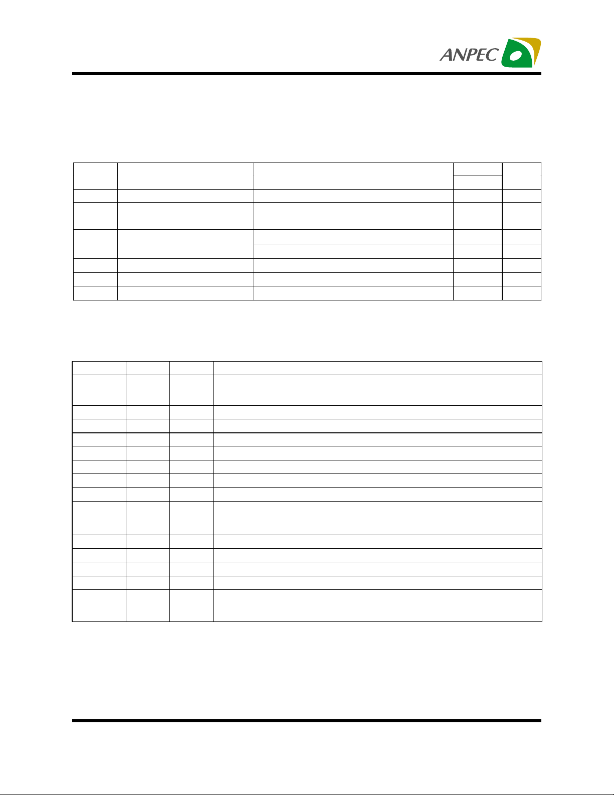
Features General Description
••
• Operating Voltage: 3.3V to 5V
••
••
• DC Volume Control Interface, 0dB to –105dB
••
••
• Depop Circuitry Integrated
••
••
• Thermal shutdown protection circuitry
••
••
• High supply voltage ripple rejection
••
••
• Low Supply Current, IDD = 13mA at Stereo BTL
••
••
• Low Shutdown Current, IDD = 0.7µA
••
••
• Bridge-Tied Load (BTL) or Single-Ended-(SE)
••
Modes Operation
••
• Output Power at 1% THD+N, VDD=5V
••
-1.2 W/Ch (typ) into an 8Ω Load
••
• Output Power at 10% THD+N, VDD=5V
••
-1.5 W/Ch (typ) into an 8Ω Load
••
• Low Crossover Distortion
••
••
• Low Quiescent Current
••
••
• Bridge-tied or Stereo(Single-ended) Configura-
••
tions
The APA7063 is a monolithic integrated circuit that provides DC volume control, and a stereo bridged audio
power amplifiers capable of producing 1.5W(1.2W) into
8Ω with less than 10%(1.0%) THD+N. APA7063 provides a volume control pin DC_Vol determines the attenuation of output of the amplifiers. The attenuator range
is from 0dB (DC_Vol=0.7VDD) to –105dB (DC_Vol=0V) with
32 steps. Both of the depop circuitry and the thermal
shutdown protection circuitry are integrated in the
APA7063, that reduces pops and clicks noise during power
up and when using the shutdown modes and protects
the chip from being destroyed by over temperature failure.
To simplify the audio system design applications, the
APA7063 combines a stereo bridge-tied loads (BTL)
mode for speaker drive and a stereo single-end (SE)
mode for headphone drive into a single chip, where both
modes are easily switched by the SE/BTL input control
pin signal. The APA7063 also features a shutdown function which keeps the supply current only 0.7µA (typ).
Applications
••
• Portable and Desktop Computers
••
••
• Multimedia Monitors
••
••
• Portable Radios, PDAs, and Portable TVs
••
ANPEC reserves the right to make changes to improve reliability or manufacturability without notice, and advise
customers to obtain the latest version of relevant information to verify before placing orders.
Copyright ANPEC Electronics Corp.
Rev. A.5 - Mar., 2003
Pin Description
SHUTDOWN
V
CC
DC Vol
Vo1
Vin1
Vin2
Vo2 V
GND
1
2
3
4
5
6
7
8
16
15
14
13
12
11
10
+ OUT1
V
CC
- OUT1
Bypass
SE/BTL
- OUT2
9
www.anpec.com.tw1
CC
+ OUT2

APA7063
Ordering and Marking Information
APA7063
APA7063 J :
APA7063 K :
APA7063
XXXXX
APA7063
XXXXX
Block Diagram
SE/BTL
Handling Code
Temp. Range
Package Code
Vo1
Vin1
Vin2
+
Bias
+
-
Package Code
J : P DIP - 1 6 K : SO P - 1 6
Temp. Range
I : - 40 to 85 C
Handling Code
TU : Tube TR : Tape & Reel
XXXXX - Date Code
XXXXX - Date Code
10K
Ω
Volume
Control
32 steps
+
20K
°
10K
Ω
20K
Ω
Ω
+
+ OUT1
- OUT1
Vo2
Shutdown
V
CC
GND
Bypass
Power
Management
Click and Pop
Suppression
Circuitry
10K
20K
+
-
Ω
+
-
20K
Ω
Ω
10K
Ω
- OUT2
+ OUT2
Absolute Maximum Ratings
(Over operating free-air temperature range unless otherwise noted.)
Symbol Parameter Rating Unit
V
DD
T
A
T
J
T
STG
T
S
V
ESD
Copyright ANPEC Electronics Corp.
Rev. A.5 - Mar., 2003
Supply Voltage 6 V
Operating Ambient Temperature Range -40 to 85
Maximum Junction Temperature 150
Storage Temperature Range -65 to +150
Soldering Temperature,10 seconds 260
Electrostatic Discharge -2000 to 2000*
1
C
°
C
°
C
°
C
°
V
www.anpec.com.tw2

APA7063
Electical Characteristics
Electrical Characteristics for Entire IC
The following specifications apply for VDD= 5V unless otherwise noted. Limits apply for TA= 25°C
Min. Typ. Max.
V
I
I
V
V
Electrical Characteristics for V olume Attenuators
The following specifications apply for VDD= 5V. Limits apply for TA= 25°C
RANGE
Supply Voltage 3.3 5.5 V
DD
Quiescent Pow e r Su pp ly
DD
VIN=0V, IO=0A 13 25 mA
Current
Shutdown Current V
SD
SE/BTL Hig h Inpu t Voltage 4 V
IH
SE/BTL Low Input Voltage 0.8 V
IL
PIN 2
= V
DD
Min. Typ. Max.
Attenuator Range
Gain with V
Attenuation wi th V
pIN 3
=5V ±0.5C
=0V -100 -105
pIN 3
APA7063Symbol Parameter Test Conditions
0.7 2.0
APA7063Symbol Parameter Test Conditions
Unit
A
µ
Unit
dB
Electrical Characteristics for BTL Mode Operation
The following specifications apply for VDD= 5V unless otherwise noted. Limits apply for TA= 25°C
V
P
Output Offset Voltage VIN=0V 5 mV
OS
Output Power
O
THD=1%, f=1kHz
R
=8
Ω
L
THD=10%, f=1kHz
=8
R
Ω
L
THD+N Total Harmonic Distortion + Noise
AVD=2, 20Hz<f<20kHz, RL=8Ω , P
=1W
P
=340mW, RL=32Ω ,
O
RSRR Power Supply Rejection Ratio
X
TALK
V
Channel S eparation
Output Noise Voltage
N
V
=200mV
RIPPLE
C
=2.2µF, f=120Hz
B
f=1kHz , C
R
=8Ω,A-Wtd Filter
L
=2.2µF
B
Rms
, RL=8
Ω
APA7063 UnitSymbol Parameter Test Conditions
Typ.
1.2
W
1.5
O
0.3
%
1.0
74 dB
95 dB
40 uV
Copyright ANPEC Electronics Corp.
Rev. A.5 - Mar., 2003
www.anpec.com.tw3
APA7063
Electical Characteristics (Cont.)
Electrical Characteristics for SE Mode Operation
The following specifications apply for VDD= 5V unless otherwise noted. Limits apply for TA= 25°C
APA7063Symbol Parameter Test Conditions
Typ.
V
THD+N Total Harmonic Distortion plus
RSRR Power Supply Rejectio n Ratio
X
Output Offset Voltage VIN=0V, 100 mV
DS
P
Output Power
O
Noise
Channel Separation
TALK
V
Output Noise Voltage
N
THD=1%, f=1KHZ, R
THD=10%, f=1KHZ, R
AV= 1,V
P
= 75mW, RL=32KΩ, Av=1, f=1KHZ
O
V
RIPPLE
f=1KHZ, C
R
=1KΩ, A-Wtd Filter
L
=1 V
OUT
= 200mV
=2.2µF
B
=32K
Ω
L
=32K
Ω
L
, f=1KHZ, RL=1K
RMS
, f=120Hz,CB=2.2µF
RMS
Ω
95
100
0.01
0.05
58
95
30
mW
Pin Description
Pin Name No I/O Description
Shutdown 1 1
VDD 2,10,15 Supply voltage input pin.
DC_Vol 3 I Volume control function input pin.
Vo1 4 O C hannel 1 output for external feedb a ck circuit.
Vin1 5 I Audio input channel 1
Vin2 6 I Audio input channel 2
Vo2 7 O C hannel 2 output for external feedb a ck circuit.
GND 8 Ground connection for circuitry.
+OUT2 9 O
-OUT2 11 O Channel 2 negative output in BTL mode and in SE mode.
SE/BTL 12 I Mode control signal input, hold low for BTL mode, hold high for SE mode.
Bypass 13 I Connect to voltage divider for internal mid_supply bias
-OUT2 14 O Channel 1 negative output in BTL mode and in SE mode.
+OUT1 16 O
Shutdown mode control signal input, place entire IC in shutdown mode
when held high, Idd=0.7uA.
Channel 2 positive output in BTL mode and high impedance state in SE
mode.
Channel 1 positive output in BTL mode and high impedance state in SE
mode.
Unit
dB
dB
uV
Copyright ANPEC Electronics Corp.
Rev. A.5 - Mar., 2003
www.anpec.com.tw4

APA7063
Typical Application Circuit
#8
R-in
L-in
R_var
r*=R_var/50
1
µµµµ
F
20k
20k
µµµµ
F
1
ΩΩΩΩ
ΩΩΩΩ
20k
1µF
ΩΩΩΩ
20k
Shutdown +OUT1
VCC VCC
DC_Vol -OUT1
Vo1 Vbypass
Vi1 SE/BTL
Vi2 -OUT2
Vo2 VCC
ΩΩΩΩ
GND +OUT2
220
R-ch
100k
L-ch
µµµµ
F
#8
ΩΩΩΩ
1k
ΩΩΩΩ
100k
ΩΩΩΩ
Headphone jack
APA7063
µµµµ
220
F
1k
ΩΩΩΩ
* Add a resistor to avoid volume control gain error at power on status. For the R_var with 10KΩ variable resistor, the recommended
value of r is in range of 100~200Ω.
Copyright ANPEC Electronics Corp.
Rev. A.5 - Mar., 2003
www.anpec.com.tw5

APA7063
Typical Characteristics
10
VDD=5V
5
RL=8Ω
Po=1.0W
2
1
0.5
BTL
VDD=5V
5
RL=16Ω
Po=0.5W
2
1
0.5
BTL
0.2
0.1
0.05
0.02
0.01
20 20k50 100 200 500 1k 2k 5k 10k
AV=2AV=8
AV=4
THD+N-Total Harmonic Distortion+Noise (%)
Frequency (Hz)
10
VDD=5V
5
RL=8Ω
2
1
0.5
0.2
0.1
0.05
BTL
f=20kHz
f=1kHz
f=20Hz
0.02
0.01
10m 220m 50m 100m 200m 500m 1
THD+N-Total Harmonic Distortion+Noise (%)
Output Power (W)
0.2
0.1
0.05
0.02
0.01
20 20k50 100 200 500 1k 2k 5k 10k
AV=4
AV=2
AV=8
THD+N-Total Harmonic Distortion+Noise (%)
Frequency (Hz)
10
VDD=5V
5
RL=16Ω
2
1
0.5
BTL
f=20kHz
0.2
0.1
0.05
0.02
0.01
10m 120m 50m 100m 200m 500m
f=1kHz
f=20Hz
THD+N-Total Harmonic Distortion+Noise (%)
Output Power (W)
Copyright ANPEC Electronics Corp.
Rev. A.5 - Mar., 2003
www.anpec.com.tw6

APA7063
Typical Characteristics (Cont.)
10
VDD=5V
5
RL=8Ω
Po=0.25W
2
1
0.5
0.2
0.1
0.05
0.02
0.01
20 20k50 100 200 500 1k 2k 5k 10k
SE
AV=1
AV=4
AV=2
THD+N-Total Harmonic Distortion+Noise (%)
Frequency (Hz)
10
VDD=5V
5
RL=10kΩ
2
Vin=1Vrms
1
0.5
0.1
0.05
0.02
0.01
0.005
0.002
0.001
SE
AV=1
AV=4
AV=2
20 20k50 100 200 500 1k 2k 5k 10k
10
VDD=5V
5
RL=32Ω
2
Po=75mW
1
0.5
0.1
0.05
0.02
0.01
0.005
0.002
0.001
SE
AV=1
AV=4
AV=2
20 20k50 100 200 500 1k 2k 5k 10k
THD+N-Total Harmonic Distortion+Noise (%)
Frequency (Hz)
10
VDD=5V
5
RL=8Ω
2
1
0.5
0.2
0.1
0.05
0.02
0.01
10m 500m20m 30m 50m 70m 200m
SE
f=20kHz
f=20Hz
f=1kHz
THD+N-Total Harmonic Distortion+Noise (%)
Froquency (Hz)
Copyright ANPEC Electronics Corp.
Rev. A.5 - Mar., 2003
THD+N-Total Harmonic Distortion+Noise (%)
Output Power (W)
www.anpec.com.tw7

APA7063
Typical Characteristics (Cont.)
10
VDD=5V
5
RL=32Ω
2
1
0.5
0.1
0.05
0.02
0.01
0.005
0.002
0.001
10m 200m20m 30m 50m 70m 100m
SE
f=20kHz
f=20Hz
f=1kHz
THD+N-Total Harmonic Distortion+Noise (%)
Output Power (W))
10
VDD=3.3V
5
RL=8Ω
Po=0.4W
2
1
0.5
BTL
10
VDD=5V
5
RL=10kΩ
2
1
0.5
0.1
0.05
0.02
0.01
0.005
0.002
0.001
100m 3200m 300m 500m 800m 1 2
SE
f=20kHz
f=1kHz
THD+N-Total Harmonic Distortion+Noise (%)
Output Voltage (V)
10
VDD=3.3V
5
RL=16Ω
Po=0.2W
2
1
0.5
BTL
f=20Hz
0.2
AV=2
0.1
0.05
0.02
0.01
20 20k50 100 200 500 1k 2k 5k 10k
AV=8
THD+N-Total Harmonic Distortion+Noise (%)
Frequency (Hz)
Copyright ANPEC Electronics Corp.
Rev. A.5 - Mar., 2003
0.2
0.1
0.05
0.02
0.01
AV=2
AV=4
20 20k50 100 200 500 1k 2k 5k 10k
AV=8
THD+N-Total Harmonic Distortion+Noise (%)
Output Power (W)
www.anpec.com.tw8

APA7063
Typical Characteristics (Cont.)
10
VDD=3.3V
5
RL=8Ω
2
1
0.5
0.2
0.1
0.05
0.02
0.01
10m 800m20m 30m 50m 80m 200m 400m
BTL
f=20kHz
f=1kHz
f=20Hz
THD+N-Total Harmonic Distortion+Noise (%)
10
VDD=3.3V
5
RL=8Ω
Po=100mW
2
1
0.5
SE
10
VDD=3.3V
5
RL=16Ω
2
1
0.5
0.2
0.1
0.05
BTL
f=20kHz
f=1kHz
f=20Hz
0.02
0.01
10m 500m20m 30m 50m 70m 200m
THD+N-Total Harmonic Distortion+Noise (%)
Output Power (W)Output Power (W)
10
VDD=3.3V
5
RL=32Ω
Po=35mW
2
1
0.5
SE
0.2
0.1
0.05
0.02
0.01
20 20k50 100 200 500 1k 2k 5k 10k
AV=1
AV=4
AV=2
THD+N-Total Harmonic Distortion+Noise (%)
Copyright ANPEC Electronics Corp.
Rev. A.5 - Mar., 2003
0.2
0.1
0.05
0.02
0.01
20 20k50 100 200 500 1k 2k 5k 10k
AV=1
AV=4
AV=2
THD+N-Total Harmonic Distortion+Noise (%)
Frequency (Hz)Frequency (Hz)
www.anpec.com.tw9

APA7063
Typical Characteristics (Cont.)
10
VDD=3.3V
5
RL=10kΩ
Vin=1Vp
2
1
0.5
0.2
0.1
0.05
0.02
SE
AV=1
AV=2
AV=4
0.01
20 20k50 100 200 500 1k 2k 5k 10k
THD+N-Total Harmonic Distortion+Noise (%)
10
VDD=3.3V
5
RL=32Ω
2
1
0.5
SE
10
VDD=3.3V
5
RL=8Ω
2
1
0.5
0.2
0.1
0.05
SE
f=20kHz
f=20Hz
f=1kHz
0.02
0.01
10m 200m20m 30m 50m 70m 100m
THD+N-Total Harmonic Distortion+Noise (%)
Output Power (W)Frequency (Hz)
10
VDD=3.3V
5
RL=10kΩ
2
1
0.5
SE
0.2
0.1
0.05
f=20kHz
f=1kHz
0.02
0.01
10m 55m12m 15m 20m 25m 30m 35m 42m
f=20Hz
THD+N-Total Harmonic Distortion+Noise (%)
Output Power (W)
Copyright ANPEC Electronics Corp.
Rev. A.5 - Mar., 2003
0.2
0.1
0.05
0.02
0.01
100m 2200m 300m 500m 700m 1
f=20kHz
f=1kHz
f=20Hz
THD+N-Total Harmonic Distortion+Noise (%)
Output Voltage (V)
www.anpec.com.tw10

APA7063
Typical Characteristics (Cont.)
10
VDD=5V
5
RL=10kΩ
2
docking
1
0.5
0.1
0.05
0.02
0.01
0.005
0.002
0.001
100m 3200m 300m 500m 800m 1 2
f=20kHz
f=1kHz
f=20Hz
THD+N-Total Harmonic Distortion+Noise (%)
Output Voltage (V)
100u
50u
20u
No filter
A_wtd filter
10
VDD=3.3V
5
RL=10kΩ
docking
2
1
0.5
0.2
0.1
0.05
0.02
0.006
100m 2200m 300m 500m 700m 1
f=20kHz
f=1kHz
f=20Hz
THD+N-Total Harmonic Distortion+Noise (%)
Output Voltage (V)
100u
50u
20u
No filter
A_wtd filter
10u
5u
VDD=5V
-Output Noise Voltage( V)
N
V
RL=8Ω
2u
Av=2V/V
BTL
1u
20 20k50 100 200 500 1k 2k 5k 10k
Frequency (Hz)
Copyright ANPEC Electronics Corp.
Rev. A.5 - Mar., 2003
10u
5u
VDD=5V
-Output Noise Voltage( V)
N
V
RL=10kΩ
2u
Av=1V/V
SE
1u
20 20k50 100 200 500 1k 2k 5k 10k
Frequency (Hz)
www.anpec.com.tw11

APA7063
Typical Characteristics (Cont.)
+0
VDD=5V
-20
RL=8Ω
Po=1W
Av=2V/V
-40
-60
-80
Crosstalk (dB)
-100
BTL
f=1kHz
f=20kHz
-120
20 20k50 100 200 500 1k 2k 5k 10k
Frequency (Hz)
+12
+10
Cf=0.22µF
+0
VDD=5V
RL=32Ω
-20
Po=75mW
Av=1V/V
-40
-60
-80
Crosstalk (dB)
-100
SE
f=1kHz
f=20kHz
-120
20 20k50 100 200 500 1k 2k 5k 10k
Frequency (Hz)
0.7
0.6
RL=8Ω
+8
Cf=0.068µF
+6
+4
Gain (dBV)
+2
-0
20 20k50 100 200 500 1k 2k 5k 10k
Cf=0.1µF
Frequency (Hz)
Copyright ANPEC Electronics Corp.
Rev. A.5 - Mar., 2003
VDD=5V
RL=8Ω
Av=2V/V
BTL
0.5
0.4
RL=16Ω
0.3
0.2
-Power Disspation (W)
D
0.1
P
0
0 0.25 0.5 0.75 1 1.25 1.5
RL=32Ω
VDD=5V
THD<1%
Output Power (W)
www.anpec.com.tw12
BTL

APA7063
4
Typical Characteristics (Cont.)
0.2
0.18
0.16
0.14
0.12
0.1
0.08
0.06
-Power Disspation (W)
0.04
D
P
0.02
0
0 0.05 0.1 0.15 0.2 0.25 0.3 0.35 0.
RL=16Ω
RL=32Ω
RL=8Ω
VDD=5V
THD<1%
Output Power (W)
2
1.8
1.6
1.4
1.2
0.8
0.6
Output Power (W)
0.4
0.2
VDD=5V
RL=8Ω
BTL
1
THD=10%
THD=1%
0
2.5 3 3.5 4 4.5 5 5.5
SE
20
No Load
17.5
15
12.5
10
7.5
5
-Supply Current (mA)
DD
I
2.5
0
11.522.533.544.555.5
BTL
SE
VDD-Supply Voltage (V)
0.16
0.14
0.12
0.1
0.08
0.06
Output Power (W)
0.04
0.02
VDD=5V
RL=32Ω
SE
THD=10%
THD=1%
0
2.5 3 3.5 4 4.5 5 5.5
VDD-Supply Voltage (V)
Copyright ANPEC Electronics Corp.
VDD-Supply Voltage (V)
www.anpec.com.tw13
Rev. A.5 - Mar., 2003

APA7063
Typical Characteristics (Cont.)
3
VDD=5V
2.5
2
1.5
1
Output Power (W)
0.5
THD=1%
0
4 8 12 16 20 24 28 32 36 40 44 48 52 56 60 64
THD=10%
Load Resistance (Ω)
1.1
1
0.9
0.8
0.7
0.6
0.5
0.4
0.3
Output Power (W)
0.2
THD=1%
0.1
0
4 8 12 16 20 24 28 32 36 40 44 48 52 56 60 64
THD=10%
VDD=3.3V
BTL
BTL
0.8
0.7
0.6
0.5
0.4
0.3
Output Power (W)
0.2
THD=1%
0.1
0
4 8 12 16 20 24 28 32 36 40 44 48 52 56 60 64
THD=10%
Load Resistance (Ω)
0.34
0.32
0.3
0.28
0.26
0.24
0.22
0.2
0.18
0.16
0.14
0.12
0.1
Output Power (W)
0.08
0.06
0.04
0.02
THD=1%
0
4 8 12 16 20 24 28 32 36 40 44 48 52 56 60 64
THD=10%
VDD=3.3V
VDD=5V
SE
SE
Load Resistance (Ω)
Copyright ANPEC Electronics Corp.
Rev. A.5 - Mar., 2003
Load Resistance (Ω)
www.anpec.com.tw14

APA7063
Typical Characteristics (Cont.)
20
VDD=5V
0
-20
-40
-60
SE
Gsin (dBV)
-80
-100
-120
0.0 0.5 1.0 1.5 2.0 2.5 3.0 3.5 4.0 4.5 5.0
Voltage (V)
+0
VDD=5V
-10
Vin=200mVp
-20
-30
-40
-50
RL=8Ω
Cb=2.2µF
SE/BTL
PRSS (dBgA)
-60
-70
-80
20 20k50 100 200 500 1k 2k 5k
Frequency (Hz)
Copyright ANPEC Electronics Corp.
Rev. A.5 - Mar., 2003
www.anpec.com.tw15

APA7063
Packaging Information
SO – 300mil ( Reference JEDEC Registration MS-013)
D
N
EH
12
3
GAUGE
PLANE
A
e
Millimet ers Variations- D Inches Variations- D
Dim
A1
φ
Min. Max. Variations Min. Max.
A2.35
0.10 0.30
0.33 0.51
B
D See variations SO-24
7.40 7.60
E
e 1.27BSC SO-14
H
L
N See variations N See variations
10°8
10 10.65
0.40 1.27
2.65
B
SO-16
SO-18
SO-20
SO-28
°φ
A1
10.10 10.50
11.35 11.76
12.60 13
15.20 15.60
17.70 18.11
8.80 9.20
Dim
A1 0.004 0.0120 SO-18 0.447 0.463
Min. Max. Variations Min. Max.
A 0.093 0.1043 SO-16 0.398 0.413
B 0.013 0.020 SO-20 0.496 0.512
D See variations SO-24 0.599 0.614
E 0.2914 0.2992 SO-28 0.697 0.713
e 0.050BSC SO-14 0.347 0.362
H 0.394 0.419
L 0.016 0.050
10°8
L
°
1
Copyright ANPEC Electronics Corp.
Rev. A.5 - Mar., 2003
www.anpec.com.tw16

APA7063
Packaging Information (Cont.)
PDIP-16 pin ( Reference JEDEC Registration MS-001)
D
L
E1
2
A
A
1
3
A
Dim
A - 5.320 - 0.210
A1 0.380 - 0.015 A2 3.169 3.422 0.125 0.135
A3 2.915 3.803 0.1 15 0.150
D 18.632 19.646 0.735 0.775
E 7.605BSC 0.300BSC
E1 6.210 6.464 0.245 0.255
L° 0 380.25 0 15
e
B
Min. Max. Min. Max.
8.492 9.506 0.335 0.375
Millimeters Inches
A
E
B
e
Copyright ANPEC Electronics Corp.
Rev. A.5 - Mar., 2003
www.anpec.com.tw17

APA7063
Physical Specifications
Ter m ina l M aterial Solder -P lated Copper (Solder Material : 90/10 or 6 3/3 7 S n Pb)
Lead Solderab ility Meets EIA Specification RSI8 6-91, A NSI/J-STD-002 Catego ry 3.
Reflow Condition
Reference JEDEC Standard J-STD-020A APRIL 1999
temperature
Pre-heat temperature
(IR/Convection or VPR Reflow)
°
183 C
Peak temperature
Time
Classification Reflow Prof iles
Convection or IR/
Convection
Average ramp-up rate(183°C to Peak) 3°C/second max. 10 °C /second max .
Preheat temperature 125 ± 25°C)
Temperature maintained above 183°C
Time within 5°C of actual peak temperature
Peak temperature range
Ramp-down rate
Time 25°C to peak temperature
120 seconds max
60 – 150 seconds
10 –20 seconds 60 seconds
220 +5/-0°C or 235 +5/-0°C 215-219°C or 235 +5/-0°C
6 °C /second max . 10 °C /second max .
6 minutes max.
VPR
Package Reflow Conditions
pkg. thickness
and all bgas
Convection 220 +5/-0 °C Convection 235 +5/-0 °C
VPR 215-219 °C VPR 235 +5/-0 °C
IR/Convection 220 +5/-0 °C IR/Convection 235 +5/-0 °C
Copyright ANPEC Electronics Corp.
Rev. A.5 - Mar., 2003
2.5mm
≥≥≥≥
pkg. thickness < 2.5mm and
pkg. volume
350 mm³
≥≥≥≥
pkg. thickness < 2.5mm and pkg.
volume < 350mm³
www.anpec.com.tw18

APA7063
Reliability test Program
Test item Method Description
SOLDERABILITY MIL-STD-883D-2003
HOLT MIL-STD-883D-1005.7
PCT JESD-22-B, A102
TST MIL-STD-883D-1011.9
ESD MIL-STD-883D-3015.7 VHBM > 2KV, VMM > 200V
Latch-Up JESD 78 10ms , Itr > 100mA
Carrier Tape & Reel Dimensions
°
C , 5 SEC
245
1000 Hrs Bias @ 125
168 Hrs, 100 % RH , 121
°
C ~ 150°C, 200 Cycles
-65
t
°
C
°
C
D1
D
Bo
Ko
T2
B
T1
E
F
W
A
Po
P
P1
Ao
J
C
Application
Copyright ANPEC Electronics Corp.
Rev. A.5 - Mar., 2003
A B C
330 ± 162 +1.5
F D
5.5± 1 1.55 +0.1 1.55+ 0.25 4.0 ± 0.1 2.0 ± 0.1 6.4 ± 0.1 5.2± 0. 1 2 .1± 0.1 0.3±0.013
12.75+
0.15
D1 Po P1 Ao Bo Ko tSOP- 8
J T1 T2 W P E
2 ± 0.5 1 2 .4 ± 0.2 2 ± 0.2 12± 0. 3 8± 0.1 1.75±0.1
www.anpec.com.tw19

APA7063
Cover Tape Dimensions
Application Carrier W idt h Cove r Tape Width De vices Per Reel
SOP- 8
Customer Service
Anpec Electronics Corp.
Head Office :
5F, No. 2 Li-Hsin Road, SBIP,
Hsin-Chu, T aiwan, R.O.C.
T el : 886-3-5642000
Fax : 886-3-5642050
Taipei Branch :
7F, No. 137, Lane 235, Pac Chiao Rd.,
Hsin Tien City, Taipei Hsien, T aiwan, R. O. C.
T el : 886-2-89191368
Fax : 886-2-89191369
12 9.3 2500
Copyright ANPEC Electronics Corp.
Rev. A.5 - Mar., 2003
www.anpec.com.tw20
 Loading...