

查询APA4880供应商
APA4880
Stereo 330mW 8Ω Speak Driver With Mute
Features
• Operating Voltage
Single Supply 3V to 7V
Dual Supply ±1.5V to ± 3.5V
• Depop Circuitry Integrated.
• High Signal-to-Noise Ratio 100dB
• High Slew Rate 5.5V/ms
• Low Distortion -66dB
• Output Power at 10% THD+N
into 8Ω 330mW
into 16Ω 200mW
• Large Output Voltage Swing
• Excellent Power Supply Ripple Rejection
• Low Power Consumption
• Short-circuit Elimination
• Wide Temperature Range
Applications
• Portable Digital Audio
• Personal Computers
• Microphone Preamplifier
• CD ROM Player
• Headphone Amplifier
Gereral Description
The APA4880 is an integrated class AB stereo headphone amplifier contained in an SO-8 or a DIP-8 plastic package. The APA4880 is capable of delivering
330mW of max. output power to an 8Ω load with less
than 10% (THD+N) from a 5V power supply. The
device has been primarily developed for portable digital audio applications. Both of the depop circuitry and
mute circuitry are integrated in the APA4880 , that
reduces pops and clicks noise during power up and
when using the mute mode(high active).
• No Switch ON/OFF Clicks
• Available in 8 pin SOP,TSSOP or PDIP
Package
Ordering and Marking Information
APA4880
Lead Free Code
Handling Code
Tem p. Range
Package Code
APA 4880 J : APA 4880
APA 4880 K/O :
ANPEC reserves the right to make changes to improve reliability or manufacturability without notice, and advise
customers to obtain the latest version of relevant information to verify before placing orders.
Copyright ANPEC Electronics Corp.
Rev. A.4 - Jan., 2003
XXXXX
APA 4880
XXXXX
Package Code
J : P DIP - 8 K : S OP - 8 O : T SS O P -8
Tem p. Range
I : - 40 to 85 C
Handling Code
TU : Tube TR : Tape & Reel
Lead Free Code
L : Lead Free Device Blank : Original Device
XXXXX - Date Code
XXXXX - Date Code
°
www.anpec.com.tw1
APA4880
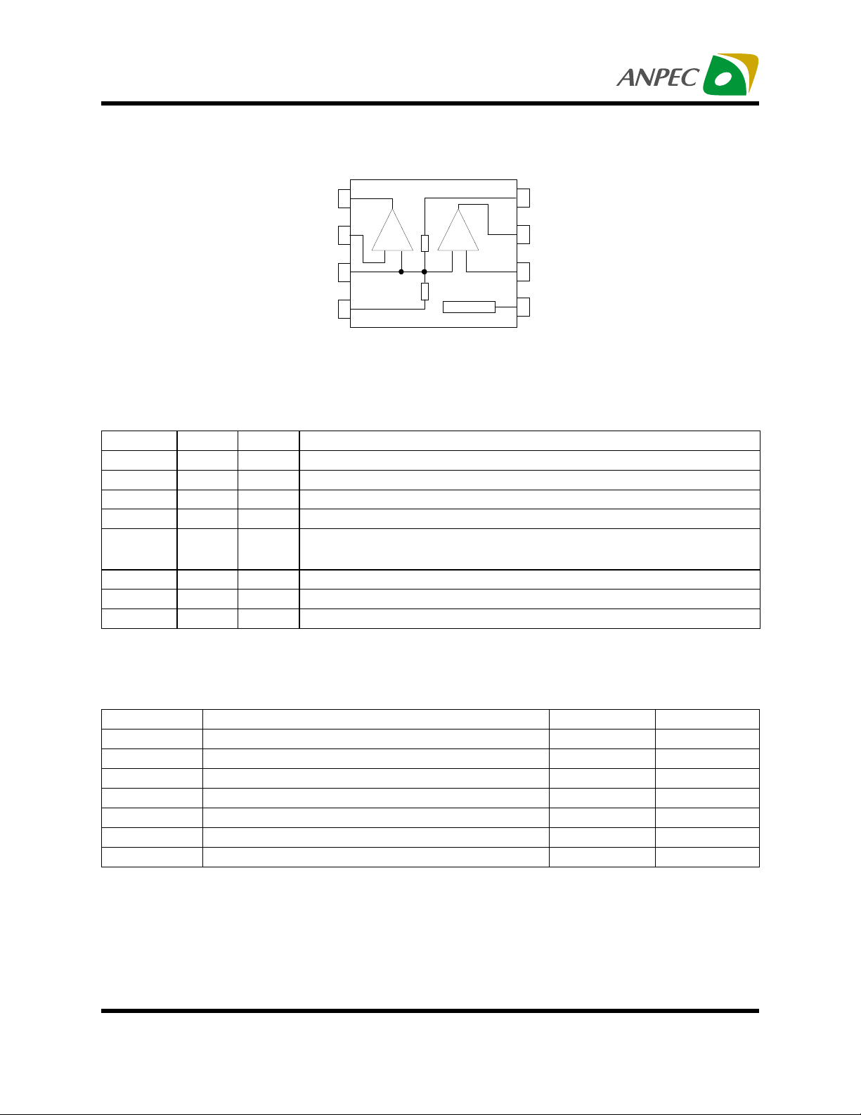
Block Diagram
OutA
INA
Bypass
V
SS
1
2
3
4
+A-
B
+-
MUTE
8V
DD
7
OutB
INB
6
Mute
5
APA4880
Pin Function Description
Pin Name No I/O Description
OUTA 1 O Channel A output pin
INA 2 I Audio input channel A
Bypass 3 I Connect to voltage divider for internal mid_supply bias
VSS 4 Ground or negative supply voltage connection for circuitry.
Mute 5 I
INB 6 I Audio input channel B
OUTB 7 O Channel B output pin
VDD 8 Supply voltage input pin
mute mode control signal input, place entire IC in mute mode when held
high, Imute=140µA
Absolute Maximum Ratings
Symbol Parameter Rating Unit
V
DD
T
SC(O)
T
A
T
J
T
STG
T
S
V
ESD
Note : *1. Human body model : C=100pF , R=1500Ω , 3 positive pulses plus 3 negative pulses
Copyright ANPEC Electronics Corp.
Rev. A.4 - Jan., 2003
Supply Voltage 5 V
Output Short-Circuit Duration , at TA=25°C , P
TOT
=1W
20 S
Operating Ambient Temperature range -40 to 85
Maximum Junction Temperature 150
Storage Temperature Range -65 to+150
Soldering Temperature , 10 seconds 260
Electrostatic Discharge -3000 to 3000
*1
www.anpec.com.tw2
C
°
C
°
C
°
C
°
V
APA4880
Thermal Characteristics
Symbol Parameter Value Unit
R
THJA
Electrical Characteristics
TA=25°C, VDD=5V, VSS=0V, f=1kHz (unless otherwise noted)
Symbol Parameter Test Conditions
I
DD
I
MUTE
V
I(OS)
AC Characteristics
(THD+N)/S Total Harmonic Distortion
Po Output Power (THD+N)/S=0.1% , f=1kHz
PSRR Power Supply Rejection
ATT Mute attenuation
Xtalk Channel Separation
Gv Open Loop Gain 100 dB
Fg Unity Gain Frequency 7 MHz
SR Slew Rate 5.5 V/us
S/N Signal to Noise Ratio
Thermal Re sistance from Ju nc t ion to Ambient in Free Air
SO-8
TSSOP-8
PDIP-8
210
220
109
APA4880
Min. Typ. Max.
Supply Current No Load 3.0 mA
Mute Current V
PINS
140 uA
Input Offset Voltage 5 mV
0.05
0.04
0.03
240
150
85
plus Noise to Signal Ratio
P
=200mW , RL=8Ω , f=1kHz
O
P
=120mW , RL=16Ω , f=1kHz
O
P
=75mW , RL=32Ω , f=1kHz
O
R
=8
Ω
L
R
=16
Ω
L
R
=32
Ω
L
(THD+N)/S=10% , f=1kHz
=8
R
Ratio
Ω
L
R
=16
Ω
L
R
=32
Ω
L
CS=2.2uF , V
RIPPLE
=200mV
f=120Hz
Vin=1Vrms , R
P
=200mV , RL=8Ω , Cb=2.2µF
O
Vin=1Vrms , R
L
L
=8
=8
Ω
Ω
RMS
,
330
200
110
50 dB
85 dB
85 dB
20 uVrm s
K/W
Unit
%
mW
Copyright ANPEC Electronics Corp.
Rev. A.4 - Jan., 2003
www.anpec.com.tw3
APA4880
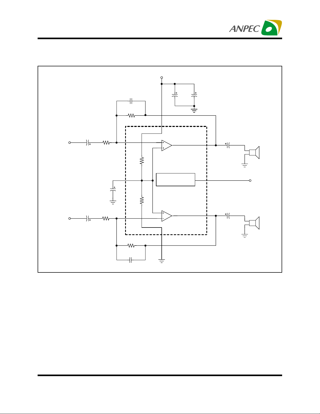
Test And Application Circuits
+5V
Vin A
Vin B
2.2
2.2
220pF
Ω
15k
8
V
µ
F
F
µ
15k
2.2µF
15k
Ω
2
INA
Ω
200k
Bypass
3
200k
Ω
Ω
6 INB
Ω
15k
DD
Click and POP
Suppression Circuit
GND
4
0.1
µ
F
100µF
OUTA
Mute
OUTB
µ
F
220
1
Mute
µ
220
7
F
Copyright ANPEC Electronics Corp.
Rev. A.4 - Jan., 2003
220pF
www.anpec.com.tw4
APA4880
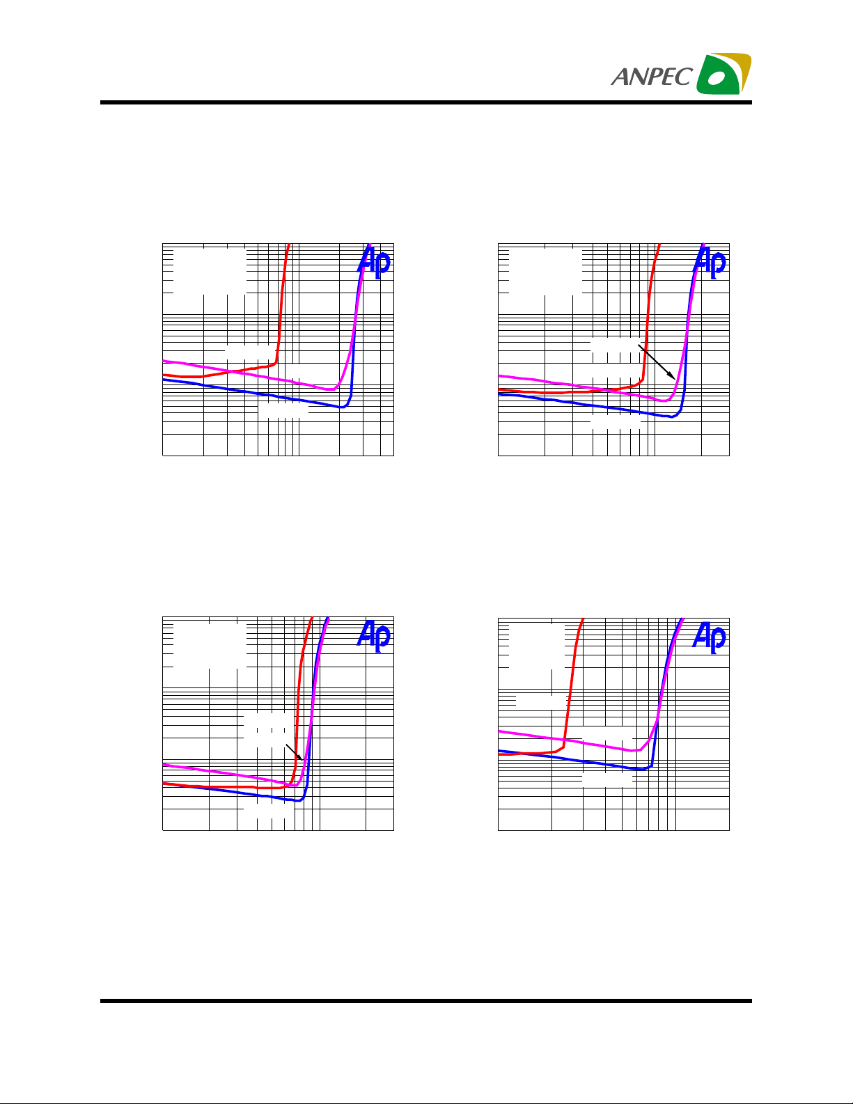
Typical Characteristics
10
VDD=5V
5
RL=8Ω
Av=-1
2
1
0.5
0.2
0.1
0.05
0.02
0.01
10m 500m20m 30m 50m 80m 200m
THD+N-Total Harmonic Distortion+Noise (%)
f=20Hz
f=1kHz
f=20kHz
Output Power (W)
VDD=5V
5
RL=32Ω
Av=-1
2
1
0.5
0.2
0.1
0.05
f=20Hz
f=20kHz
10
VDD=5V
5
RL=16Ω
Av=-1
2
1
0.5
0.2
0.1
0.05
0.02
0.01
10m 300m20m 30m 50m 70m 100m
THD+N-Total Harmonic Distortion+Noise (%)
f=20kHz
f=20Hz
f=1kHz
Output Power (W)
10
VDD=3V
5
RL=8Ω
Av=-1
2
1
f=20Hz
0.5
0.2
0.1
0.05
f=20kHz
f=1kHz
0.02
0.01
10m 300m20m 30m 50m 70m 100m
THD+N-Total Harmonic Distortion+Noise (%)
f=1kHz
Output Power (W)
Copyright ANPEC Electronics Corp.
Rev. A.3 - Jun., 2001
0.02
0.01
10m 200m20m 30m 50m 70m 100m
THD+N-Total Harmonic Distortion+Noise (%)
Output Power (W)
www.anpec.com.tw5
APA4880
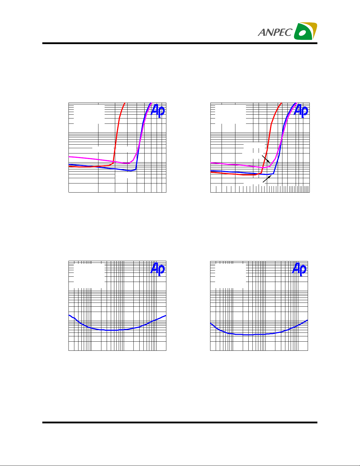
Typical Characteristics Cont.
10
VDD=3V
5
RL=16Ω
Av=-1
2
1
0.5
0.2
0.1
0.05
0.02
0.01
10m 100m20m 30m 40m 50m 70m
THD+N-Total Harmonic Distortion+Noise (%)
f=20kHzf=20Hz
f=1kHz
Output Power (W)
10
VDD=5V
5
RL=8Ω
Po=200mW
2
Av=-1
1
0.5
10
VDD=3V
5
RL=32Ω
Av=-1
2
1
0.5
0.2
0.1
0.05
0.02
0.01
10m 45m12m 15m 20m 25m 30m 35m
THD+N-Total Harmonic Distortion+Noise (%)
f=20Hz
f=20kHz
f=1kHz
Output Power (W)
10
VDD=5V
5
RL=16Ω
Po=120mW
2
Av=-1
1
0.5
0.2
0.1
0.05
0.02
0.01
20 20k50 100 200 500 1k 2k 5k
THD+N-Total Harmonic Distortion+Noise (%)
Frequency (Hz)
Copyright ANPEC Electronics Corp.
Rev. A.3 - Jun., 2001
0.2
0.1
0.05
0.02
0.01
20 20k50 100 200 500 1k 2k 5k
THD+N-Total Harmonic Distortion+Noise (%)
Frequency (Hz)
www.anpec.com.tw6
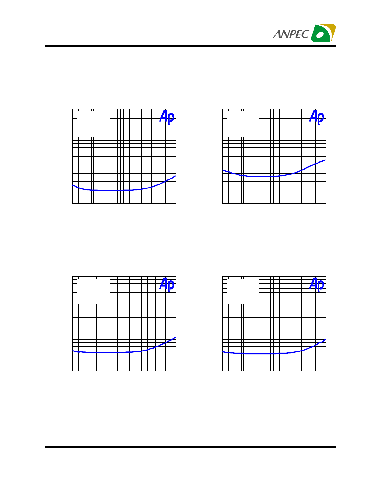
APA4880
Typical Characteristics Cont.
10
VDD=5V
5
RL=32Ω
Po=70mW
2
Av=-1
1
0.5
0.2
0.1
0.05
0.02
0.01
20 20k50 100 200 500 1k 2k 5k
THD+N-Total Harmonic Distortion+Noise (%)
Frequency (Hz)
10
VDD=3V
5
RL=16Ω
Po=50mW
2
Av=-1
1
0.5
10
VDD=3V
5
RL=8Ω
Po=70mW
2
Av=-1
1
0.5
0.2
0.1
0.05
0.02
0.01
20 20k50 100 200 500 1k 2k 5k
THD+N-Total Harmonic Distortion+Noise (%)
Frequency (Hz)
10
VDD=3V
5
RL=32Ω
Po=25mW
2
Av=-1
1
0.5
0.2
0.1
0.05
0.02
0.01
20 20k50 100 200 500 1k 2k 5k
THD+N-Total Harmonic Distortion+Noise (%)
Frequency (Hz)
Copyright ANPEC Electronics Corp.
Rev. A.3 - Jun., 2001
0.2
0.1
0.05
0.02
0.01
20 20k50 100 200 500 1k 2k 5k
THD+N-Total Harmonic Distortion+Noise (%)
Frequency (Hz)
www.anpec.com.tw7
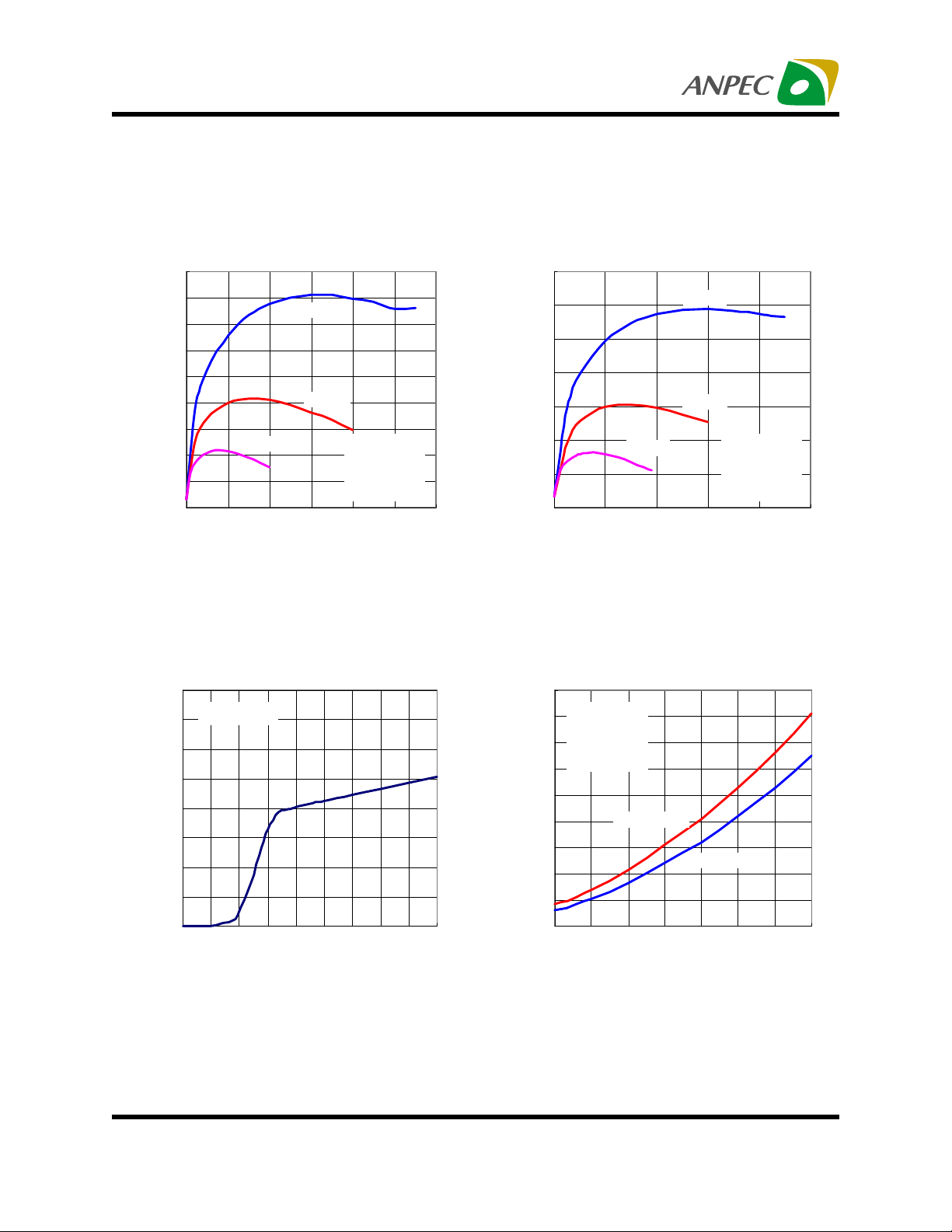
APA4880
Typical Characteristics Cont.
180
160
RL=8Ω
140
120
100
80
60
40
-Power Disspation (mW)
D
P
20
0
0 50 100 150 200 250 300
RL=32Ω
RL=16Ω
VDD=5V
Av=-1
f=1kHz
BW<80kHz
Output Power (mW)
4
3.5
2.5
Idd (mA)
1.5
0.5
No Load
3
2
1
0
1 1.5 2 2.5 3 3.5 4 4.5 5 5.5
70
60
50
40
30
20
-Power Disspation (mW)
D
10
P
RL=32Ω
RL=8Ω
RL=16Ω
VDD=3V
Av=-1
f=1kHz
BW<80kHz
0
0 20 40 60 80 100
Output Power (mW)
450
400
350
300
250
200
150
Output Power (mW)
100
50
Av=-1
f=1kHz
RL=8Ω
BW<80kHz
THD+N=10%
THD+N=1%
0
2 2.5 3 3.5 4 4.5 5 5.5
Vdd (V)
Copyright ANPEC Electronics Corp.
Rev. A.3 - Jun., 2001
VDD-Supply Voltage (V)
www.anpec.com.tw8

APA4880
Typical Characteristics Cont.
300
Av=-1
250
f=1kHz
RL=16Ω
200
150
BW<80kHz
THD+N=10%
100
Output Power (mW)
50
0
2 2.5 3 3.5 4 4.5 5 5.5
THD+N=1%
VDD-Supply Voltage (V)
350
300
250
200
150
100
Output Power (mW)
50
THD+N=10%
THD+N=1%
BW<80kHz
VDD=5V
Av=-1
f=1kHz
160
140
120
100
80
Av=-1
f=1kHz
RL=32Ω
BW<80kHz
THD+N=10%
60
40
Output Power (mW)
20
0
2 2.5 3 3.5 4 4.5 5 5.5
THD+N=1%
VDD-Supply Voltage (V)
120
VDD=3V
100
Av=-1
f=1kHz
80
60
BW<80kHz
THD+N=10%
40
Output Power (mW)
20
THD+N=1%
0
816243240485664
Load Resistance (Ω)
Copyright ANPEC Electronics Corp.
Rev. A.3 - Jun., 2001
0
816243240485664
Load Resistance (Ω)
www.anpec.com.tw9

APA4880
Typical Characteristics Cont.
40u
VDD=5V
35u
30u
25u
20u
Vn (Vrms)
15u
10u
5u
0
20 20k50 100 200 500 1k 2k 5k
Av=-1
RL=8Ω
22Hz<BW<22kHz
Frequency (Hz)
+0
-10
-20
-30
VDD=5V
Av=-1
Vpp=200mV
RL=8Ω
Cb=2.2uF
+0
VDD=5V
-20
Av=-1
Po=200mW
RL=8Ω
-40
-60
Xtalk (dB)
-80
-100
-120
20 20k50 100 200 500 1k 2k 5k
B to A
A to B
Frequency (Hz)
+0
VDD=5V
-20
-40
Av=-1
Vin=1Vrms
RL=8Ω
mute mode
-40
-50
PSRR (dB)
-60
-70
-80
20 100k50 100 200 500 1k 2k 5k 10k 20k
Frequency (Hz)
Copyright ANPEC Electronics Corp.
Rev. A.3 - Jun., 2001
-60
Gain (dBV)
-80
-100
-120
20 20k50 100 200 500 1k 2k 5k
Frequency (Hz)
www.anpec.com.tw10
APA4880
φ
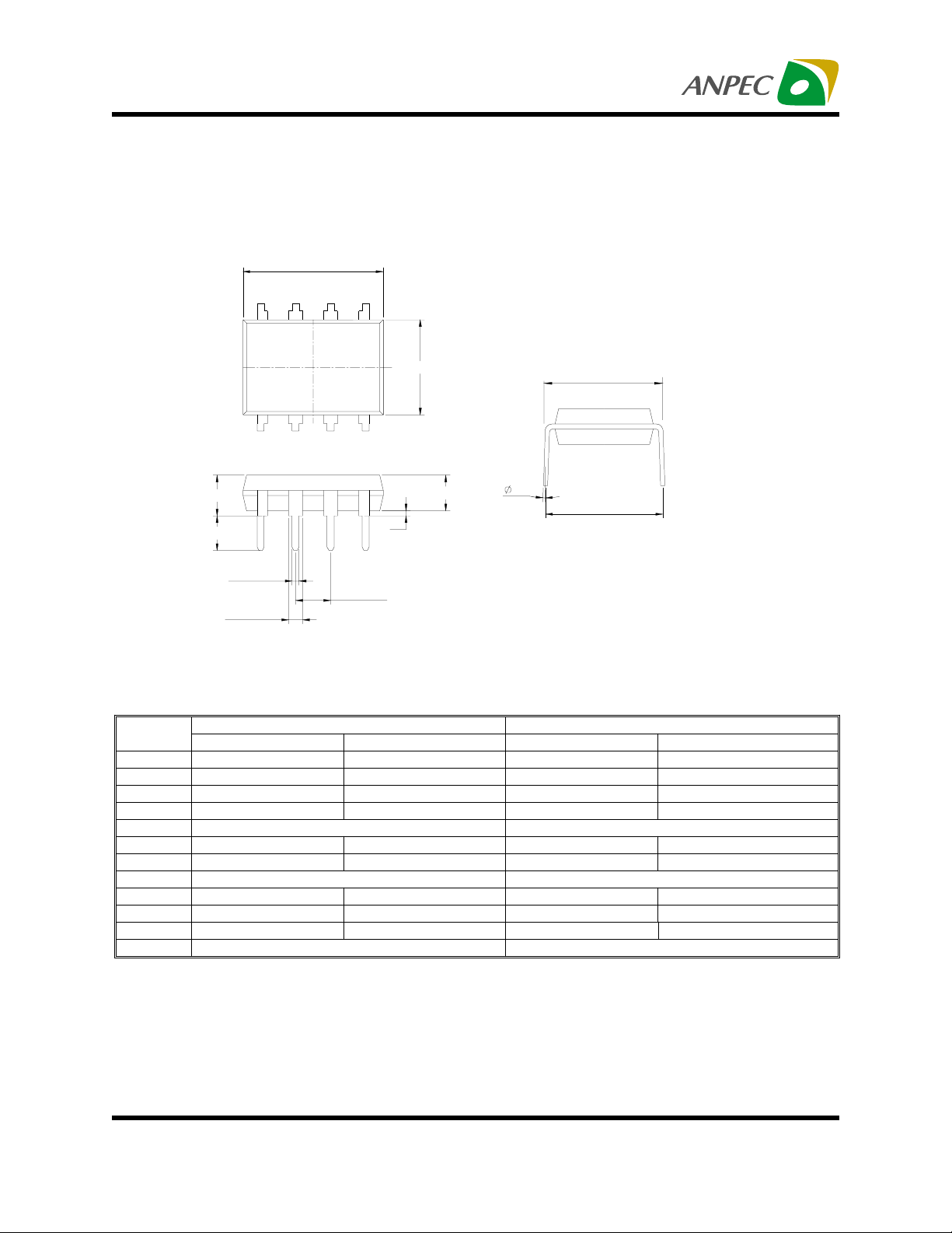
Packaging Information
PDIP-8 pin ( Reference JEDEC Registration MS-001)
D
E1
1
A
L
e2
e 3
A1
e 1
A2
Millimeters InchesDim
Min. Max. Min. Max.
A
A1
A2
D
e1
e2
e3
E
E1
0.38 0.015
2.92 3.68 0.115 0.145
9.02 10.16 0.355 0.400
2.54BSC 0.100BSC
0.36 0.56 0.014 0.022
1.14 1.78 0.045 0.070
7.62 BSC 0.300 BSC
6.10 7.11 0.240 0.280
E3
L
115
2.92 3.81 0.115 0.150
°
5.33 0.210
10.92 0.430
E
1
E3
15
°
Copyright ANPEC Electronics Corp.
Rev. A.4 - Jan., 2003
www.anpec.com.tw11

APA4880
Packaging Information
SOP-8 pin ( Reference JEDEC Registration MS-012)
HE
0.015X45
e1 e2
D
A1
A
1
L
0.004max.
Dim
A 1.35 1.75 0.053 0.069
A1 0.10 0.25 0.004 0.010
D 4.80 5.00 0.189 0.197
E 3.80 4.00 0.150 0.157
H 5.80 6.20 0.228 0.244
L 0. 40 1.27 0.016 0.050
e1 0.33 0.51 0.013 0.020
e2 1.27BSC 0.50BSC
18
φ
Millimeters Inches
Min. Max. Min. Max.
°
8
°
Copyright ANPEC Electronics Corp.
Rev. A.4 - Jan., 2003
www.anpec.com.tw12

APA4880
φ
φ
φ
Packaging Information
TSSOP-8
e
8
7
2 x E / 2
(2)
S
(L1)
GAUGE
PLANE
L
1
Dim
12
b
E1 E
e/2
D
A2
A
A1
0.25
(3)
Millimeters Inches
Min. Max. Min. Max.
A 1.2 0.047
A1 0.00 0.15 0.000 0.006
A2 0.80 1.05 0.031 0.041
b 0.19 0.30 0.007 0.012
D 2.9 3.1 0.114 0.122
e 0.65 BSC 0.026 BSC
E 6.40 BSC 0.252 BSC
E1 4.30 4.50 0.169 0.177
L 0.45 0.75 0.018 0.030
L1 1.0 REF 0.039REF
R 0.09 0.004
R1 0.09 0.004
S 0.2 0.008
10
212
312
°
REF 12° REF
°
REF 12° REF
°
8
°
0
°
8
°
Copyright ANPEC Electronics Corp.
Rev. A.4 - Jan., 2003
www.anpec.com.tw13

APA4880
Physical Specifications
Terminal Ma ter ial Solder-Plated Copper (Solder Mater ial : 90/10 or 63/37 S nPb ), 100 %Sn
Lead Solderability Meets EIA Specification RSI86- 91 , AN SI/J- S T D-002 Category 3.
Reflow Condition (IR/Convection or VPR Reflow)
T
P
Ramp-up
T
L
Tsmax
Tsmin
Tempe rature
ts
Preheat
25
°
t 25 C to Pe a k
Classificatin Reflow Profiles
tp
Ramp-down
Time
Critical Zone
to T
T
L
P
t
L
Profile Feature
Average ramp-up rate
(T
to TP)
L
Preheat
- Temperature Min (Tsmin)
- Temperature Mix (Tsmax)
- Time (min to max)(ts)
Tsmax to T
L
Sn-Pb Eutectic Assembly Pb-Free Assembly
Large Body Small Body Large Body Small Body
3°C/second max. 3°C/second max.
100°C
150°C
60-120 seconds
- Ramp-up Rate
Tsmax to TL
- Temperature(T
- Time (t
)
L
Peak Temperature(Tp)
Time within 5°C of actual Peak
Temperature(tp)
Ramp-down Rate
Time 25°C to Peak Temperature
Note: All temperatures refer to topside of the package. Measured on the body surface.
Copyright ANPEC Electronics Corp.
Rev. A.4 - Jan., 2003
)
L
60-150 seconds
225 +0/-5°C 240 +0/-5°C 245 +0/-5°C 250 +0/-5°C
10-30 seconds 10-30 seconds 10-30 seconds 20-40 seconds
6°C/second max. 6°C/second max.
6 minutes max. 8 minutes max.
183°C
150°C
200°C
60-180 seconds
3°C/second max
217°C
60-150 seconds
www.anpec.com.tw14
APA4880
Reliability Test Program
Test item Method Description
SOLDERABILITY MIL-STD-883D-2003
HOLT MIL-STD-883D-1005.7
PCT JESD-22-B,A102
TST MIL-STD-883D-1011.9
ESD MIL-STD-883 D- 301 5.7 VHBM > 2KV, VMM > 200V
Latch-Up JESD 78 10ms, 1tr > 100mA
Carrier Tape & Reel Dimensions
245°C, 5 SEC
1000 Hrs Bias @125°C
168 Hrs, 100%RH, 121°C
-65°C~150°C, 200 Cycles
t
Application
SOP- 8
Application
TSSOP-8
D1
D
Bo
Ko
T2
B
T1
E
F
W
A
A B C J T1 T2 W P E
330 ± 162 +1.5
F D D1 Po P1 Ao Bo Ko t
5.5± 1 1.55 +0.1 1.55+ 0.25 4.0 ± 0.1 2.0 ± 0.1 6.4 ± 0.1 5.2± 0. 1 2.1± 0.1 0.3±0.013
A B C J T1 T2 W P E
330 ± 162 +1.5
F D D1 Po P1 Ao Bo Ko t
Po
12.75+
0.15
12.75+
0.15
P
P1
Ao
J
C
2 ± 0.5 12.4 ± 0.2 2 ± 0.2 12± 0. 3 8± 0.1 1.75±0.1
2 + 0.5 12.4 ± 0.2 2 ± 0.2 12± 0. 3 8± 0.1 1.75±0.1
5.5 ± 0. 1 1.5 + 0.1 1.5 + 0.1 4.0 ± 0.1 2.0 ± 0.1 7.0 ± 0.1 3.6 ± 0.3 1.6 ± 0.1 0.3±0.013
(mm)
Copyright ANPEC Electronics Corp.
Rev. A.4 - Jan., 2003
www.anpec.com.tw15

APA4880
Cover Tape Dimensions
Applicatio n Carrier W id t h Cover Tape Wid t h Devices P e r R eel
SOP- 8
TSSOP- 8
Customer Service
Anpec Electronics Corp.
Head Office :
5F, No. 2 Li-Hsin Road, SBIP,
Hsin-Chu, Taiwan, R.O.C.
Tel : 886-3-5642000
Fax : 886-3-5642050
Taipei Branch :
7F, No. 137, Lane 235, Pac Chiao Rd.,
Hsin Tien City, Taipei Hsien, Taiwan, R. O. C.
Tel : 886-2-89191368
Fax : 886-2-89191369
12 9.3 2500
12 9.3 2500
Copyright ANPEC Electronics Corp.
Rev. A.4 - Jan., 2003
www.anpec.com.tw16
 Loading...