


Copyright ANPEC Electronics Corp.
Rev. A.3 - Apr., 2001
APA4863
www.anpec.com.tw1
ANPEC reserves the right to make changes to improve reliability or manufacturability without notice, and advise
customers to obtain the latest version of relevant information to verify before placing orders.
Stereo 2.2W Audio Power Amplifier
Features
••
••
•
Depop Circuitry Integrated
••
••
•
Thermal Shutdown Circuitry Integrated
••
••
•
Bridge-Tied Load (BTL) or Single-Ended
(SE) Modes Operation
••
••
•
Output Power at 1% THD+N, VDD=5V
- 2.2W/Ch (typ) into a 3 Ω Load
- 1.8W/Ch (typ) into a 4 Ω Load
- 1.2 W/Ch (typ) into a 8 Ω Load
••
••
• Shutdown Control Mode, I
SD
= 0.5 µA
••
••
• Output Power (SE) at 0.5% THD+N, V
DD
=5V
- 90mW/Ch (typ.) into a 32Ω Load
••
••
• Various Power Packages Available
SOP, TSSOP, TSSOP-P
Applications
••
••
• Stereo Audio Power Amplifier for Notebook
Computer
••
••
• Portable Televisions
••
••
• Portable and Desktop Computers
General Description
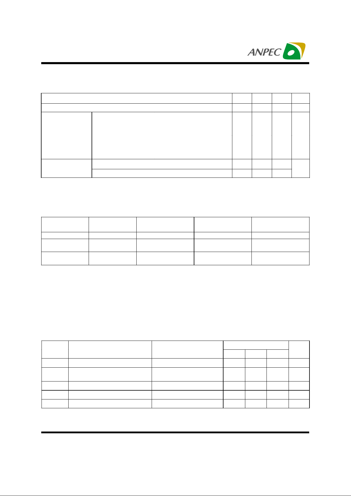
Ordering Information
The APA4863 is a stereo bridge-tied audio power amplifier in various power packages , including SOP ,
TSSOP and TSSOP-P . When connecting to a 5V voltage supply , the APA4863 is capable of delivering
2.2W/1.8W/1.2W of continuous RMS power per channel into 3Ω/4Ω/8Ω bridge-tied loads with less than
1% THD+N respectively . When APA4863 operates
in the single-ended load , it is capable of delivering
90mW of continuous RMS power per channel into
32Ω load . The APA4863 simplifies design and frees
up board space for other features .
The APA4863 also served well in low-voltage applications , which provides 750mW (1% THD+N) per
channel into 4Ω loads with a 3.3V supply voltage .
Both of the depop circuitry and the thermal shutdown
protection circuitry are integrated in the APA4863 ,
that reduces pops and clicks noise during power up
and when using the shutdown mode and protects the
chip from being destroyed by over-temperature failure . To simplify the audio system design in notebook computer applications , the APA4863 combines
a stereo bridge-tied loads mode for speaker drive and
a stereo single-end mode for headphone drive into a
single chip , where both modes are easily switched
by the HP-IN input control pin signal . For power sensitive applications , the APA4863 also features a shutdown function which keeps the supply current only
0.5 µA (typ.) .
Package Code
K: SOP
O: TSSOP R: TSSOP-P*
Temp. Range
I : -40 to 85 C
Handling Code
TU : Tube
TR : Tape & Reel TY: Tray
APA4863
Handling Code
Temp. Range
Package Code
°
* TSSOP-P is a standard TSSOP package with a thermal pad exposed on the bottom of the package.

Copyright ANPEC Electronics Corp.
Rev. A.3 - Apr., 2001
APA4863
www.anpec.com.tw2
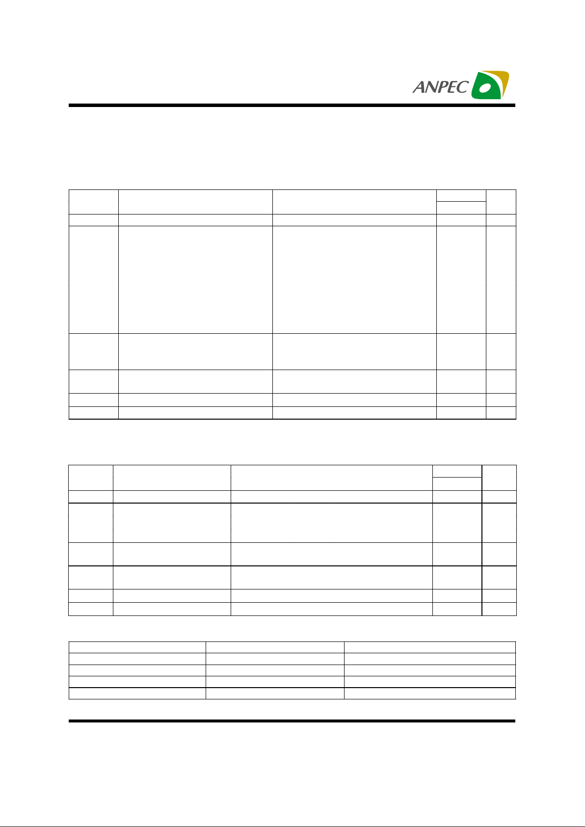
Block Diagram
(Over operating free-air temperature range unless otherwise noted.)
Absolute Maximum Ratings
Ring
10
4, 13
V
DD
5
0ΚΩ
50K
Ω
+
+
5
3
- IN A
+ OUT A
R
L
100µF
To HP-IN Circuit
8
Ω
20K
Ω
20K
Ω
20K
Ω
+
+
12
14
+ OUT B
R
L
8
Ω
20K
Ω
20K
Ω
20K
Ω
- OUT B
- OUT A
C
O
+
1K
Ω
100µF
C
O
+
1K
Ω
C
S
0.1µF
V
DD
/ 2
6
C
B
2.2µF
8 + IN A*
Bypass
11
9
- IN B
+ IN B*
GND
2,7,15
20K
Ω
R
F
20K
Ω
R
F
C
1
R
1
Audio
Input
20K
Ω
1 µF
C
1
R
1
Audio
Input
20K
Ω
1 µF
16
1
100K
Ω
Shutdown
HP-IN
To Control Pin on
Headphone Jack
1
00ΚΩ
Headphone Jack
Sleeve
Control
Pin
Tip
V
DD
* +INA and +INB pins are connected to Bypass pin inside the IC.
Note: *1. Human body model : C=100pF, R=1500Ω, 3 positive pulses plus 3 negative pulses
Symbol Parameter Rating Unit
V
DD
Sup ply Voltage 6 V
T
A
Operating Ambient Temperature Range -40 to 85
°
C
T
J
Maximum Junction Temperature 150
°
C
T
STG
Storage Temperature Range -65 to +150
°
C
T
S
Soldering Temperature,10 seconds 260
°
C
V
ESD
Electrostatic Discharge -2000 to 2000
*1
V
Copyright ANPEC Electronics Corp.
Rev. A.3 - Apr., 2001
APA4863
www.anpec.com.tw3
Min. Typ. Max. Unit
Supply Voltag e, V
DD
355.5V
VDD=5V,
250mW/Ch average
power
4-Ω stereo BTL drive , with
proper PCB design
-20 85Operatin g fr ee-air
temper atu r e , T
A
VDD=5V,
1.8 W/Ch average
power
4-Ω stereo BTL drive , with
proper PCB design and 300
CFM forced-a ir coo ling
-20 85
°
C
VDD=5 V 1.25 4.5Common mode
input vo lt age, V
ICM
VDD=3.3V 1.25 2.7
V
Recommended Operating Conditions
Dissipation Rating Table
Package Air Flow
(CFM)
Thermal Resistance
θθθθ
JA
(°°°°C/W)
T
A
≤≤≤≤25°°°°CT
A
=70°°°°C
SO16 + 0 50 2.5W 1.6W
TSSOP ++ 0
200
73.2
66.6
1.7W
1.8W
1.1W
1.2W
TSSOP-P ++ 0
200
37.6
32.3
3.3W
3.8W
2.1W
2.4W
+ : The parameter is measured with the recommended copper heat sink pattern on an 2-layer PCB, 11.7 in
2
3.0×2.4 in2 in PCB,
1oz. copper, 3.0×1.5 in2 in coverage at Top-layer and Bottom-layer at 100% coverage (7.2in2).
++:The parameter is measured with the JEDEC standard test boards (multi-layer PCB).
APA4863
Symbol Parameter Test Conditions
Min. Typ. Max.
Unit
V
DD
Supply Voltage 3 5.5 V
I
DD
Quiescent Power Supply
Current
VIN=0V, IO=0A, HP-IN=0V
V
IN
=0V, IO=0A, HP-IN=4V
9
5
13.5
7.5
mA
I
SD
Shutdown Current V
PIN1
= V
DD
50.5
µ
A
V
IH
Headphone High Input Voltage 4 V
V
IL
Headphone Low Input Voltage 0.8 V
Electical Characteristics
Electrical Characteristics for Entire IC
The following specifications apply for VDD= 5V unless otherwise noted. Limits apply for TA= 25°C
Copyright ANPEC Electronics Corp.
Rev. A.3 - Apr., 2001
APA4863
www.anpec.com.tw4
Truth Table for Logic Inputs
Shutdown HP-IN APA4863 Mode
Low Low Bridge -Tied
Low High Single-Ended
High Low APA4863 Shutdown
High High APA4863 Shutdown
Electical Characteristics Cont.
APA4863Symbol Parameter Test Conditions
Typ.
Unit
V
OS
Output Offset Voltage VIN=0V 5 mV
THD=0.5% , f=1kHz,
R
L
=32
Ω
90
THD=1%, f=1kHz,
R
L
=8
Ω
320
P
O
Output Power
THD=10%, f=1kHz,
R
L
=8
Ω
400
mW
THD+N Total Harmonic Distortion
plus Noise
A
V
= -1 , PO=75mW, f=1kHz, RL=32
Ω
0.02 %
RSRR Power Supply Rejection
Ratio
V
RIPPLE
=200mV
RMS
, f=1kHz, CB=2.2µF, RL=8
Ω
49 dB
X
TALK
Channel Separation
f=1kHz , C
B
=2.2µF, PO=32mW, RL=32
Ω
85 dB
SNR Sig nal - to- N oise Ratio
V
DD
=5V , PO =340mW, RL=8
Ω
95 dB
Electrical Characteristics for SE Mode Operation
The following specifications apply for VDD= 5V unless otherwise noted. Limits apply for TA= 25°C
Electrical Characteristics for BTL Mode Operation
The following specifications apply for VDD= 5V unless otherwise noted. Limits apply for TA= 25°C
APA4863 UnitSymbol Parameter Test Conditions
Typ.
V
OS
Output Offset Voltage VIN=0V 5 mV
THD=1% , f=1kHz
R
L
=3
Ω
R
L
=4
Ω
R
L
=8
Ω
2.2
1.8
1.2
P
O
Output Power
THD=10% , f=1kHz
R
L
=3
Ω
R
L
=4
Ω
R
L
=8
Ω
2.7
2.3
1.5
W
THD+N Total Harmonic Distortion + Noise AVD=2, f= 1 k Hz
R
L
=4Ω , PO=1.8W
R
L
=8Ω , PO =1W
0.3
0.15
%
RSRR Power Supply Rejection Ratio
V
DD
=5V, V
RIPPLE
=200Mv
Rms
, RL=8
Ω
C
B
=2.2µF
64 dB
X
TALK
Channel Separation
f=1k Hz , C
B
=2.2µF, PO=1W, RL=8
Ω
90 dB
SNR Signal-to-Noise Ratio
V
DD
=5V, PO =1.1 W, RL=8
Ω
95 dB

Copyright ANPEC Electronics Corp.
Rev. A.3 - Apr., 2001
APA4863
www.anpec.com.tw5
Pin Description
1
2
3
4
5
6
7
8
12
11
10
9
16
15
14
13
+ OUT A
SHUTDOWN
GND
V
DD
- IN A
- OUT A
GND
+ IN A
HP-IN
GND
V
DD
- IN B
- OUT B
BYPASS
+ IN B
+ OUT B
1
2
3
4
5
6
7
8
12
11
16
15
14
13
+ OUT A
SHUTDOWN
GND
V
DD
- IN A
- OUT A
GND
+ IN A
HP-IN
GND
V
DD
- IN B
- OUT B
BYPASS
+ IN B
+ OUT B
9
10
20
19
18
17
NC
NC
NC
NC
Top View
for SOP
Top View
for TSSOP
1
2
3
4
5
6
7
8
12
11
16
15
14
13
+ OUT A
SHUTDOWN
GND
V
DD
- IN A
- OUT A
GND
+ IN A
HP-IN
GND
V
DD
- IN B
- OUT B
BYPASS
+ IN B
+ OUT B
9
10
20
19
18
17
GND
GND
GND
GND
Thermal
Pad
Pin Description
Bottom View
Top View
for TSSOP -P
for TSSOP-P
Name I/O Description
GND Ground conn ect io n of cir cuitry
V
DD
I Supply v ol tage inpu t
+ INA I Non-inve rting in put of c h annel A, connecte d to bypa s s pi n in sid e th e IC
- INA I Input pin of channel A
+ OUT A O A chann el + out put in BTL mode, hig h im pedance in SE mode
- OUT A O A channel - outpu t i n BTL mode, + outp ut in SE mode
+ IN B I Non- i nve rti ng in put of c h annel B, connected to by pa s s pi n in s id e th e IC
- IN B I Input pin of channel B
+ OUT B O B chann el + out put in BTL mode, hig h im pedance in SE mode
- OUT B O B channel - outpu t i n BTL mode, + outp ut in SE mode
BYPASS Connect to voltage divider for internal mid-supply bias
HP-IN I Headphone control pin input, hold high for single-ended mode operation
SHUTDO WN I Shutdown mode control pin inpu t, plac e s e ntir e IC in s hutdown mode
when held hig h, I
DD
= 0.5µA

Copyright ANPEC Electronics Corp.
Rev. A.3 - Apr., 2001
APA4863
www.anpec.com.tw6
Typical Characteristics
10m 3100m 1
0.01
10
0.1
1
20Hz
20kHz
1kHz
VDD=5V, RL=4
Ω
BW<80kHz
Figure 1 : Output Power (W)
Figure 2 : Frequency (Hz)
THD+N vs Output Power
THD+N (%)
0.01
10
0.1
1
20 20k100 1k 10k
VDD=5V, PO=1.8W
R
L
=4
Ω,
BW<80kHz
THD+N vs Frequency
THD+N (%)
0
0.4
0.8
1
1.2
1.4
0.6
0.2
0 0.5 1 1.5 2 2.5
0.01
10
0.1
1
20 20k100 1k 10k
AVD=10
AVD=2
VDD=5V, PO=1W
R
L
=8
Ω,
BTL Mode
Figure 4 : Frequency (Hz)
Power Dissipation vs Output Power
Power Dissipation (W)
THD+N vs Frequency
THD+N (%)
RL=4
ΩΩ
ΩΩ
Ω
VDD=5V
RL= 8
ΩΩ
ΩΩ
Ω
Figure 3 : Output Power (W)

Copyright ANPEC Electronics Corp.
Rev. A.3 - Apr., 2001
APA4863
www.anpec.com.tw7
Typical Characteristics Cont.
0.001
10
0.1
1
20 20k100 10k1k
VDD=5V, PO=150mW
R
L
=16
Ω,
SE Mode
AV= -5
AV= -1
0.001
10
0.1
1
20 20k100 1k 10k
VDD=5V, PO=75mW
RL=32
Ω,
SE Mode
AV= -5
AV= -1
Figure 5 : Frequency (Hz)
Figure 6 : Frequency (Hz)
THD+N vs Frequency
THD+N (%)
THD+N vs Frequency
THD+N (%)
0.01
10
0.1
1
10m 2100m 1
VDD=5V, RL=8
Ω
AVD=2, BW< 80kHz
BTL Mode
f= 20Hz
f= 20kHz
f= 1kHz
0.001
10
0.1
1
10m 500m70m 200m
VDD=5V, RL=16
Ω
AV=-1, BW< 80kHz
SE Mode
f= 20Hz
f= 20kHz
f= 1kHz
THD+N vs Output Power
Figure 7 : Output Power (W)
THD+N (%)
THD+N vs Output Power
Figure 8 : Output Power (W)
THD+N (%)

Copyright ANPEC Electronics Corp.
Rev. A.3 - Apr., 2001
APA4863
www.anpec.com.tw8
Typical Characteristics Cont.
0.001
10
0.1
1
10m 200m100m50m
VDD=5V, RL=32
Ω
AV=-1, BW< 80kHz
SE Mode
f= 20Hz
f= 20kHz
f= 1kHz
10m 2100m 1
VDD=3.3V, RL=4
Ω
AVD= 2
f= 20Hzf= 20kHz
f= 1kHz
0.01
10
0.1
1
Figure 9 : Output Power (W)
THD+N vs Output Power
THD+N (%)
THD+N vs Output Power
THD+N (%)
0.01
10
0.1
1
10m 1100m
VDD=3.3V, RL=8Ω,
A
VD
=2
f= 20Hz
f= 20kHz
f= 1kHz
0.01
10
0.1
1
20 20k100 1k 10k
VDD=3.3V, PO=700mW
R
L
=4Ω, AVD=2
THD+N vs Frequency
Figure 11 : Frequency (Hz)
THD+N (%)
THD+N vs Output Power
THD+N (%)
Figure 10 : Output Power (W)
Figure 12 : Output Power (W)

Copyright ANPEC Electronics Corp.
Rev. A.3 - Apr., 2001
APA4863
www.anpec.com.tw9
Typical Characteristics Cont.
0.01
10
0.1
1
20 20k100 1k 10k
VDD=3.3V, PO=450mW
R
L
=8Ω, AVD=2
0
0.05
0.1
0.15
0.2
010203040
VDD=3.3V, f=1kHz
A
VD
=2, BW<80kHz
THD+N = 10%
THD+N = 1%
Figure 13 : Frequency (Hz)
THD+N vs Frequency
THD+N (%)
Output Power vs Load Resistance
Figure 14 : Load Resistance (Ω)
Output Power (W)
Power Dissipation vs Output Power Output Power vs Supply Voltage
0
0.05
0.1
0.15
0.2
0.25
0.3
0.35
0
0.2
0.4 0.6 0.8
VDD=3.3V, SE Mode
RL=8
Ω
RL=16
Ω
0
0.25
0.5
0.75
1
1.25
1.5
1.75
2
2 2.5 3 3.5 4 4.5 5 5.5
VDD=5V, f=1kHz
R
L
=8
Ω,
BW<80kHz
BTL Mode
THD+N = 10%
THD+N = 1%
Figure 15 : Output Power (W)
Power Dissipation (W)
Figure 16 : Supply Voltage (V)
Output Power (W)

Copyright ANPEC Electronics Corp.
Rev. A.3 - Apr., 2001
APA4863
www.anpec.com.tw10
Typical Characteristics Cont.
2 2.5 3 3.5 4 4.5 5 5.5
0
50
100
150
200
250
300
VDD=5V, f=1kHz
R
L
=16
Ω,
BW<80kHz
SE Mode
THD+N = 10%
THD+N = 1%
2 2.5 3 3.5 4 4.5 5 5.5
130
150
-10
10
30
50
70
90
110
VDD=5V, f=1kHz
R
L
=32
Ω,
BW<80kHz
SE Mode
THD+N = 10%
THD+N = 1%
Figure 17
Supply Voltage (V)
Output Power vs Supply Voltage
Output Power
Figure 18
Supply Voltage (V)
Output Power vs Supply Voltage
Output Power
8182838485868
0
0.25
0.5
0.75
1
1.25
1.5
1.75
VDD=5V, f=1kHz
A
VD
=2, BW<80kHz
BTL Mode
10% THD+N
1% THD+N
0
10 20 30 40 50
60
70
0
0.2
0.4
0.6
0.8
1
VDD=5V, f=1kHz
AV=-1, BW<80kHz
SE Mode
10% THD+N
1% THD+N
Output Power vs Load Resistance
Figure 19 : Load Resistance (Ω)
Output Power (W)
Output Power vs Load Resistance
Figure 20 : Load Resistance (Ω)
Output Power (W)

Copyright ANPEC Electronics Corp.
Rev. A.3 - Apr., 2001
APA4863
www.anpec.com.tw11
Typical Characteristics Cont.
0 0.5 1 1.5
0
0.2
0.4
0.6
0.8
1
1.2
1.4
RL=8
Ω
VDD=5V, f=1kHz
THD+N <1%
BW<80kHz
BTL Mode
RL=4
Ω
RL=32
Ω
RL=16
Ω
0 0.1 0.2 0.3 0.4
0.5
0
0.02
0.04
0.06
0.08
0.1
0.12
0.14
0.16
0.18
RL=8
Ω
RL=32
Ω
RL=16
Ω
VDD=5V, f=1kHz
THD+N <1%
BW<80kHz
SE Mode
Figure 21
Output Power (W)
Power Dissipation vs Output Power
Power Dissipation
Figure 22
Output Power (W)
Power Dissipation vs Output Power
Power Dissipation
20 20k100 1k 10k
-120
-100
-80
+0
-60
-40
-20
VDD=5V, RL=8
Ω
AVD=2, PO=1W
C
B
=1µF
BTL Mode
Channel B to A
Channel A to B
1
100
10
20 20k100 10k
VO+ + VO-
VO-
VDD=5V, RL=8
Ω
AVD=2, CB=1µF
1k
Noise Floor
Figure 23 : Frequency (Hz)
Output Noise Voltage (µV)
Channel Separation
Figure 24 : Frequency (Hz)
Channel Separation (dB)

Copyright ANPEC Electronics Corp.
Rev. A.3 - Apr., 2001
APA4863
www.anpec.com.tw12
Typical Characteristics Cont.
20 20k100 1k 10k
-120
+0
-100
-80
-60
-40
-20
VDD=5V, RL=32
Ω
AV=-1, PO=75mW
C
B
=1µF
SE Mode
Channel B to A
Channel A to B
10M1k 10k 100k
+0
+80
+10
+20
+30
+40
+50
+60
+70
VDD=5V
SE Mode
Gain
Phase
1M100
Channel Separation
Figure 25 : Frequency (Hz)
Channel Separation (dB)
Open Loop Frequency Response
Figure 26 : Frequency (Hz)
Gain (dB)
2 2.5 3 3.5 4 4.5 5 5.5
0
2
4
6
8
10
VIN=0V
No Load
BTL Mode
(HP-IN=GND)
SE Mode
(HP-IN=V
DD
)
Supply Current vs Supply Voltage
Figure 27 : Supply Voltage(V)
Supply Current (mA)

Copyright ANPEC Electronics Corp.
Rev. A.3 - Apr., 2001
APA4863
www.anpec.com.tw13
Packaging Information
TSSOP/ TSSOP-P ( Reference JEDEC Registration MO-153)
Millimeters InchesDim
Min. Max. Min. Max.
A 1.2 0.047
A1 0.00 0.15 0.000 0.006
A2 0.80 1.05 0.031 0.041
D 6.4 (N=20PIN)
7.7 (N=24PIN)
6.6 (N=20PIN)
7.9 (N=24PIN)
0.252 (N=20PIN)
0.303 (N=24PIN)
0.260 (N=20PIN)
0.311 (N=24PIN)
D1 2.20 (N=20PIN)
2.70 (N=24PIN) Thermally Enhanced
0.087 (N=20PIN)
0.106 (N=24PIN) Thermally Enhanced
e 0.65 B S C 0.026 BS C
E 6.4 0 B S C 0.252 BSC
E1 4.30 4.50 0.169 0.177
E2 1.50 0.059
L 0.45 0.75 0.018 0.030
L1 1.0 REF 0.039REF
R 0.09 0.004
R1 0.09 0.004
S 0.2 0.008
φ
10
°
8
°
0
°
8
°
φ
212
°
REF 12° REF
φ
312
°
REF 12° REF
E2
BOTTOM VIEW
(THERMALLY ENHANCED VARIATIONDS ONLY)
b
D1
A1
A2
A
D
e
2 x E / 2
E1 E
e/2
N
12
3
EXPOSED THERMAL
PAD ZONE
L
(L1)
(3)
R
R1
S
(2)
0.25
GAUGE
PLANE
1

Copyright ANPEC Electronics Corp.
Rev. A.3 - Apr., 2001
APA4863
www.anpec.com.tw14
Packaging Information
SO – 300mil ( Reference JEDEC Registration MS-013)
Millimeters Variations- D Inche s Variations- D
Dim
Min. Max. Variations Min. Max.
Dim
Min. Max. Variations Min. Max.
A2.35
2.65
SO-16
10.10 10.50
A 0.093 0.1043 SO-16 0.398 0.413
A1
0.10 0.30
SO-18
11.35 11.76
A1 0.004 0.0120 SO-18 0.447 0.463
B
0.33 0.51
SO-20
12.60 13
B 0.013 0.020 SO-20 0.496 0.512
D See variations SO-24
15.20 15.60
D See variations SO-24 0.599 0.614
E
7.40 7.60
SO-28
17.70 18.11
E 0.2914 0.2992 SO-28 0.697 0.713
e1.27BSCSO-14
8.80 9.20
e 0.050BSC SO-14 0.347 0.362
H
10 10.65
H 0.394 0.419
L
0.40 1.27
L 0.016 0.050
N See variations N See variations
φ
10°8
°φ
10°8
°
N
12
3
EH
D
L
GAUGE
PLANE
1
e
B
A1
A

Copyright ANPEC Electronics Corp.
Rev. A.3 - Apr., 2001
APA4863
www.anpec.com.tw15
Reference JEDEC Standard J-STD-020A APRIL 1999
Reflow Condition (IR/Convection or VPR Reflow)
Physical Specifications
Pre-heat temperature
183 C
Peak temperature
Time
°
temperature
Classificatio n Reflow Prof ile s
Convection or IR/
Convection
VPR
Average ramp-up rate(183°C to Peak) 3°C/second max. 10 °C /second max.
Preheat temperature 125 ± 25°C)
120 seconds max
Temperature maintained above 183°C
60 – 150 seconds
Time within 5°C of actual peak temperature
10 –20 seconds 60 seconds
Peak temperature range
220 +5/-0°C or 235 +5/-0°C 215-219°C or 235 +5/-0°C
Ramp-down rate
6 °C /second max. 10 °C /second max.
Time 25°C to peak temperature
6 minutes max.
Package Reflow Conditions
pkg. thickness ≥≥≥≥ 2.5mm
and all bgas
pkg. thickness < 2.5mm and
pkg. volume ≥≥≥≥ 350 mm³
pkg. thickness < 2.5mm and pkg.
volume < 350mm³
Convection 220 +5/-0 °C Convection 235 +5/-0 °C
VPR 215-219 °C VPR 235 +5/-0 °C
IR/Convection 220 +5/-0 °C IR/Convection 235 +5/-0 °C
Term inal Material Solder-Plated Copper (Solder Material : 90/10 or 63/37 SnPb)
Lead Solderability Meets EIA Specificatio n RSI86-91, ANSI/J-S TD-002 Category 3.
Packaging 2000 devices per reel

Copyright ANPEC Electronics Corp.
Rev. A.3 - Apr., 2001
APA4863
www.anpec.com.tw16
Application
A B C J T1 T2 W P E
SOP-16W
330±3100 ± 2
13 + 0.5
2 ± 0.5
16.4 +0.3
-0.2
2.5± 0.5 16 ± 0.2 1 2± 0.1 1.75± 0.1
Application
F D D1 Po P1 Ao Bo Ko t
SOP-16W
7.5 ± 0.1
1.5 +0.1 1.5 +0.25
4.0 ± 0.1 2.0 ± 0.1 10.9 ± 0.1 10.8± 0.1 3.0± 0.1 0.3±0.013
(mm)
Carrier Tape & Reel Dimensions
A
J
B
T2
T1
C
t
Ao
E
W
Po
P
Ko
Bo
D1
D
F
P1
Cover Tape Dimensions
Carrier Width
16
Cover Tape Width
13.3
(mm)
Reliability tes t p ro g ram
Test item Method Description
SOLDERABILITY MIL-STD-883D-2003
245°C , 5 SEC
HOLT MIL-STD-883D-1005.7
1000 Hrs Bias @ 125 °C
PCT JESD-22-B, A102
168 Hrs, 100 % RH , 121°C
TST MIL-STD-883D-1011.9
-65°C ~ 150°C, 200 Cycles
ESD MIL-STD-883D-3015.7 VHBM > 2KV, VMM > 200V
Latch-Up JESD 78 10ms , Itr > 100mA

Copyright ANPEC Electronics Corp.
Rev. A.3 - Apr., 2001
APA4863
www.anpec.com.tw17
Analog and Power Electronics Corp.
Head Office :
5F, No. 2 Li-Hsin Road, SBIP,
Hsin-Chu, Taiwan, R.O.C.
Tel : 886-3-5642000
Fax : 886-3-5642050
Taipei Branch :
24F-1. No. 268, Sec. 2, PeiHsin Rd.
HsinDian, Taipei County, Taiwan, R. O. C.
Tel : 886-2-86658533
Fax : 886-2-86658529
Customer Service
 Loading...