Evaluation Board User Guide
p
UG-364
One Technology Way • P. O . Box 9106 • Norwood, MA 02062-9106, U.S.A. • Tel : 781.329.4700 • Fax : 781.461.3113 • www.analog.com
Evaluating the AD5933 1 MSPS, 12-Bit Impedance Converter Network Analyzer
FEATURES
Full-featured evaluation board for the AD5933
Graphic user interface software with frequency sweep
capability for board control and data analysis
Various power supply linking options
Standalone capability with serial I
2
C loading from on-board
microcontroller
Selectable system clock options including internal RC
oscillator or on-board 16 MHz crystal
APPLICATIONS
Electrochemical analysis
Impedance spectroscopy
Complex impedance measurement
Corrosion monitoring and protection equipment
Biomedical and automotive sensors
Proximity sensing
GENERAL DESCRIPTION
This user guide describes the EVAL-AD5933EBZ evaluation board,
and the application software developed to interface with the device.
The AD5933 is a high precision impedance converter system that
combines an on-board frequency generator with a 12-bit, 1 MSPS
analog-to-digital converter (ADC). The frequency generator
allows an external complex impedance to be excited with a
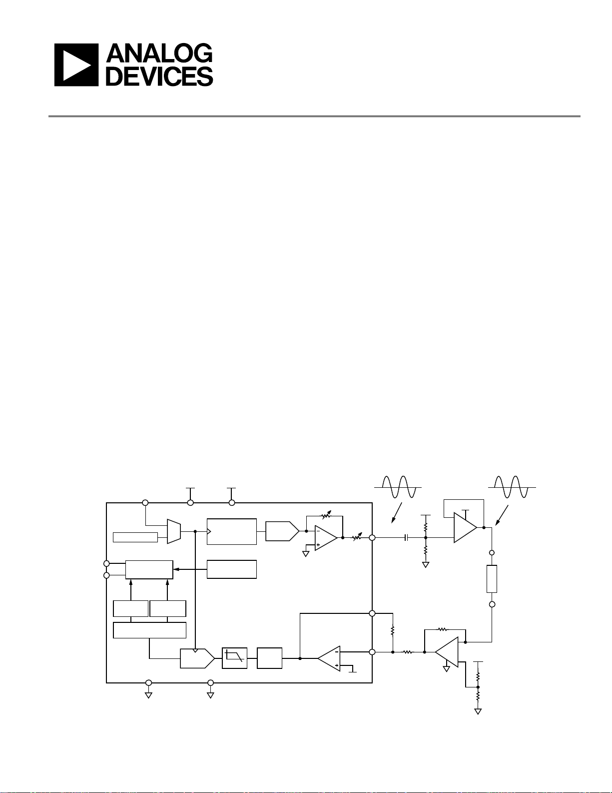
EVALUATION BOARD BLOCK DIAGRAM
V
DD
MCLK
OSCILLATOR
SCL
SDA
PLEASE SEE THE LAST PAGE FOR AN IMPORTANT
WARNING AND LEGAL TERMS AND CONDITIONS.
I2C
INTERFACE
IMAGINARY
REAL
REGISTER
REGISTER
1024-POINT DFT
AGND DGND
ADC
(12 BITS)
Rev. 0 | Page 1 of 28
V
DD
DVDDAVD D
DDS
CORE
(27 BITS)
TEMPERATURE
SENSOR
AD5933
LPF
DAC
GAIN
OUTPUT AMPLIFIER
Figure 1.
known frequency. The on-board ADC samples the response
signal from the impedance, and an on-board DSP engine at each
excitation frequency processes the DFT. The AD5933 also contains
an internal temperature sensor with 13-bit resolution. The part
operates from a 2.7 V to 5.5 V supply. Other on-board components
include a ADR423 3.0 V reference to act as a stable supply voltage
for the separate analog and digital sections of the device and a
ADP3303 ultrahigh precision regulator to act as a supply to the
on-board universal serial bus controller that interfaces to the
AD5933. The user has the option to power the entire circuitry
from the USB port of a computer.
The evaluation board also has a high performance trimmed
16 MHz surface-mount crystal to act as a system clock to the
AD5933, if required. The various link options located around the
evaluation board are listed in Table 1 . Interfacing to the AD5933
is through a USB microcontroller that generates the I
necessary to communicate with the AD5933. Interfacing to the
USB microcontroller is done through a Visual Basic® graphic user
interface located on and run from the PC. Complete specifications
for the AD5933 are available in the AD5933 data sheet available
from Analog Devices, Inc., and should be consulted in conjunction
with this user guide when using the evaluation board.
TRANSMIT SI DE
I-V
R
VDD/2
1.48V
OUT
1.98V p-p
VOUT
RFB
VIN
47nF
20kΩ
20kΩ
V
DD
50kΩ
50kΩ
A1, A2 ARE
½
AD8606
V
DD
−
A1
+
R
FB
−
A2
+
VDD/2
V
DD
50kΩ
50kΩ
1.98V p-
Z
UNKNOWN
2
C signals
10441-001

UG-364 Evaluation Board User Guide
TABLE OF CONTENTS
Features.............................................................................................. 1
Applications....................................................................................... 1
General Description ......................................................................... 1
Evaluation Board Block Diagram................................................... 1
Revision History ............................................................................... 2
Evaluation Board Hardware............................................................ 3
Terminal Block Functions ........................................................... 3
Getting Started.................................................................................. 4
Setup Sequence Summary........................................................... 4
Installing the Software ................................................................. 4
Connecting the USB Cable.......................................................... 5
Verifying the Links and Power Up the Evaluation Board ....... 6
REVISION HISTORY
2/12—Revision 0: Initial Version
Performing a Frequency Sweep ...................................................6
Two Installation Frequently Asked Questions ....................... 10
Source Code for Impedance Sweep.............................................. 12
Evaluation Board Source Code Extract................................... 13
Gain Factor Calculation ............................................................ 17
Temperature Measurement ....................................................... 17
Impedance Measurement Tips ................................................. 18
Evaluation Board Schematics and Artwork................................ 23
Ordering Information.................................................................... 26
Bill of Materials........................................................................... 26
Related Links............................................................................... 27
Rev. 0 | Page 2 of 28

Evaluation Board User Guide UG-364
EVALUATION BOARD HARDWARE
TERMINAL BLOCK FUNCTIONS
Table 1. Link Functions
Link No. Default Location Function
LK1 Out Option to remove external conditioning
LK2 Out Option to remove external conditioning
LK3 In On-board, 16 MHz crystal connection, connects to Y2
LK4 Out SMB connected external clock
LK5 In Connects 5 V from USB to ADP3303
LK6 A AVDD and DVDD power supply connector
Rev. 0 | Page 3 of 28
UG-364 Evaluation Board User Guide
GETTING STARTED
SETUP SEQUENCE SUMMARY
The evaluation board installation instructions are for the
Windows XP® operating system with English (United States) set
for its language. The regional and language settings of a PC can
be changed in the Regional and Language directory within the
Control Panel (Start/Control Panel/Regional and Language/
Formats). The installation consists of the following steps that
are described in detail in the sections that follow.
1. Install the AD5933 graphical user interface software on the
CD that accompanies the evaluation board. Do not connect
the USB cable from the AD5933 evaluation board to the
computer USB hub until the evaluation software is properly
installed. See the Installing the Software section for
additional information.
2. Connect the computer USB port to the evaluation board
using the USB cable provided in the evaluation kit and run
the USB hardware installation wizard after the evaluation
software is correctly installed (the hardware installation
may happen automatically depending on the settings of the
current operating system). See the Connecting the USB
Cable section for additional information.
3. Ensure that the appropriate links are made throughout
the evaluation board. Prior to opening and running the
evaluation software program, power up the evaluation
board appropriately. See the Verifying the Links and Power
Up section for additional information.
4. Configure the front panel of the evaluation board software to
run the required sweep function. See the Performing a
Frequency Sweep section for additional information.
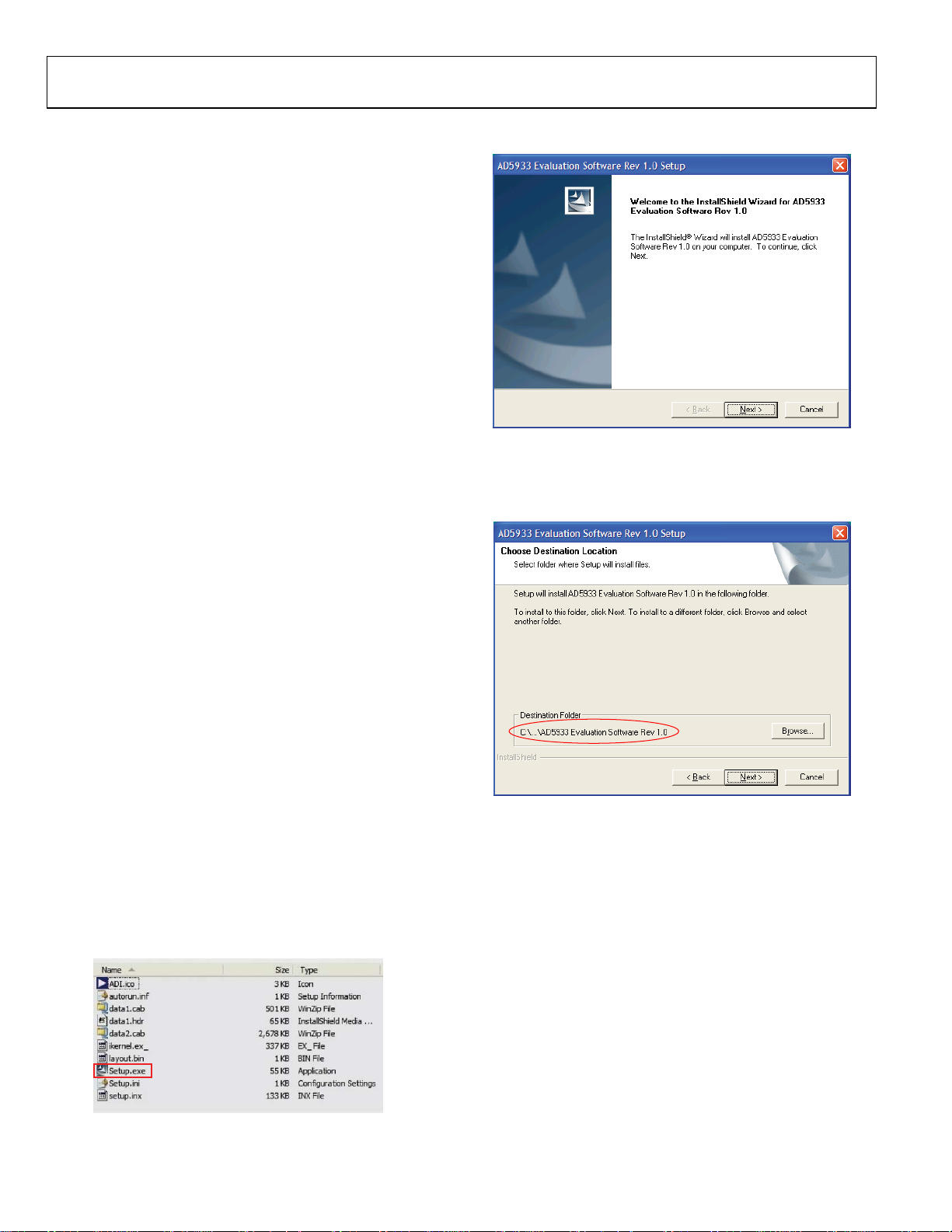
3. Install the evaluation board software in the default destination
folder path, C:\Program Files\Analog Devices\AD5933\
AD5933 Evaluation Software Rev 1.0 Setup (see Figure 4).
Figure 3. Installation Wizard
10441-004
INSTALLING THE SOFTWARE
To install the evaluation board software, use the following steps:
1. Put the evaluation board CD into the CD drive of the PC
and click Start/My Computer.
2. The CD software installation may happen automatically
after the CD is inserted into the CD drive; however, this may
depend on the settings of the current operating system. If the
software installation does not automatically start, go to
AD5933 Installation/Setup.exe and double-click Setup.exe
to install the software on the PC through the installation
wizard (see Figure 2 and Figure 3).
10441-003
Figure 2. Evaluation Software CD Contents
Rev. 0 | Page 4 of 28
10441-005
Figure 4. Default Destination Folder
Evaluation Board User Guide UG-364
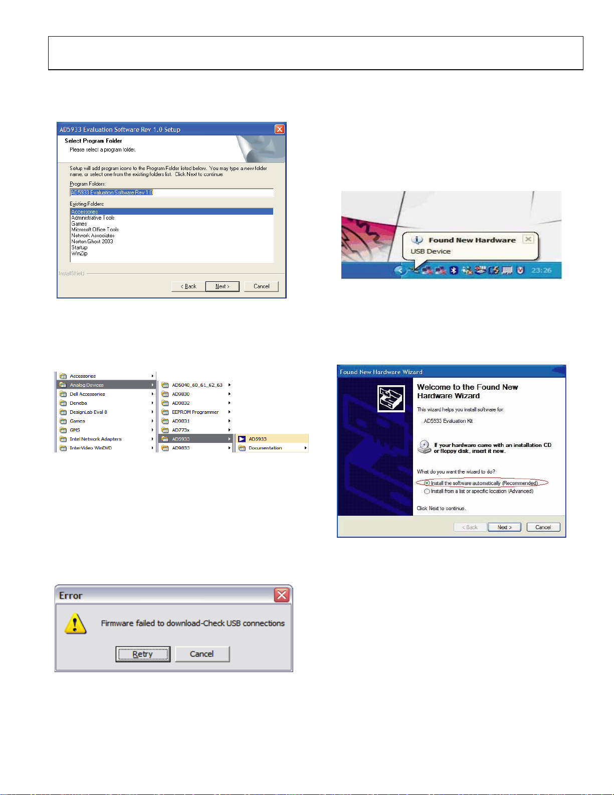
4. Choose the Analog Devices directory (see Figure 5). If the
Analog Devices folder does not yet exist, create an Analog
Devices folder and add the program icon to this new folder.
Figure 5. Select Analog Devices Directory
5. After installing the software, remove the CD from the CD
drive. You may be asked to reboot the computer at this stage.
6. Go to Start/All Programs/Analog Devices/AD5933/
AD5933 (see Figure 6).
10441-006
CONNECTING THE USB CABLE
To connect the USB cable, use the following steps:
1. Plug the USB cable into the USB hub of the PC and connect
the other end of the USB cable into the AD5933 evaluation
board USB socket (see J1 in Figure 32). A message may
appear that a USB device has been detected on the host
computer and that new hardware has been found (see
Figure 8).
10441-009
Figure 8. USB Device Detected by Host Computer
2. The Found New Hardware Wizard then appears (see
Figure 9). This wizard locates and installs the appropriate
driver files for the AD5933 evaluation kit in the operating
system registry. Select Install the software automatically
(Recommended) and click Next > to continue (see Figure 9).
Figure 6. Opening the Evaluation Software
The following message appears (see Figure 7) because the
firmware code that the evaluation software operates from,
and that needs to be downloaded to the evaluation board USB
microcontroller memory each time the interface software
program is opened, cannot be successfully downloaded to
the evaluation board. The error message is presented because
there is currently no USB connection between the computer
and the AD5933 evaluation board at this stage; therefore,
this error message is to be expected. Click Cancel.
Figure 7. Expected Error Message
10441-007
10441-008
Rev. 0 | Page 5 of 28
Figure 9. Hardware Installation Wizard
10441-010
UG-364 Evaluation Board User Guide
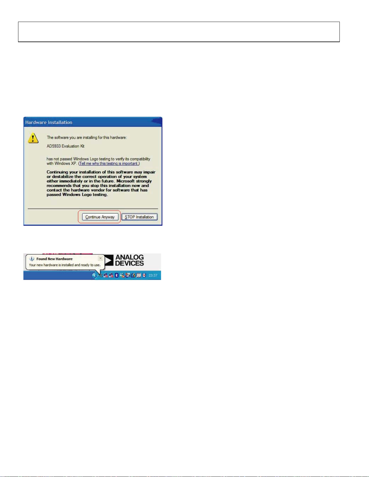
3. A standard windows operating system warning message
then appears, as shown in Figure 10. It indicates that the
new hardware currently being installing on the Windows®
operating system (AD5933 evaluation kit) has not passed the
Windows logo testing to verify compatibility with Windows
XP. This warning appears because the installation is an
evaluation setup installation and is not intended to be used
in a production environment. Click Continue Anyway and
then click Finish.
Figure 10. Expected Warning Message
The message shown in Figure 11 appears once the hardware has
been successfully installed.
Figure 11. Successful Hardware Installation
VERIFYING THE LINKS AND POWER UP THE EVALUATION BOARD
Ensure that the relevant links are in place on the evaluation board
(see Tabl e 1) and that the proper power connections and supply
values have been made to the terminal blocks before applying
power to the evaluation board. The power supply terminal blocks
are outlined in evaluation board schematic (see Figure 32). Note
that the USB connector only supplies power to the Cypress USB
controller chip that interfaces to the AD5933. If required, a
dedicated external voltage supply to each terminal block can
be provided. Ensure that all relevant power supply connections
and links are made before running the evaluation software. For
optimum performance, supply the three supply signals (A
A
VDD2
, and D
) from a stable external reference supply via the
VDD
power supply terminal blocks on the board.
,
VDD1
Rev. 0 | Page 6 of 28
10441-011
10441-012
PERFORMING A FREQUENCY SWEEP
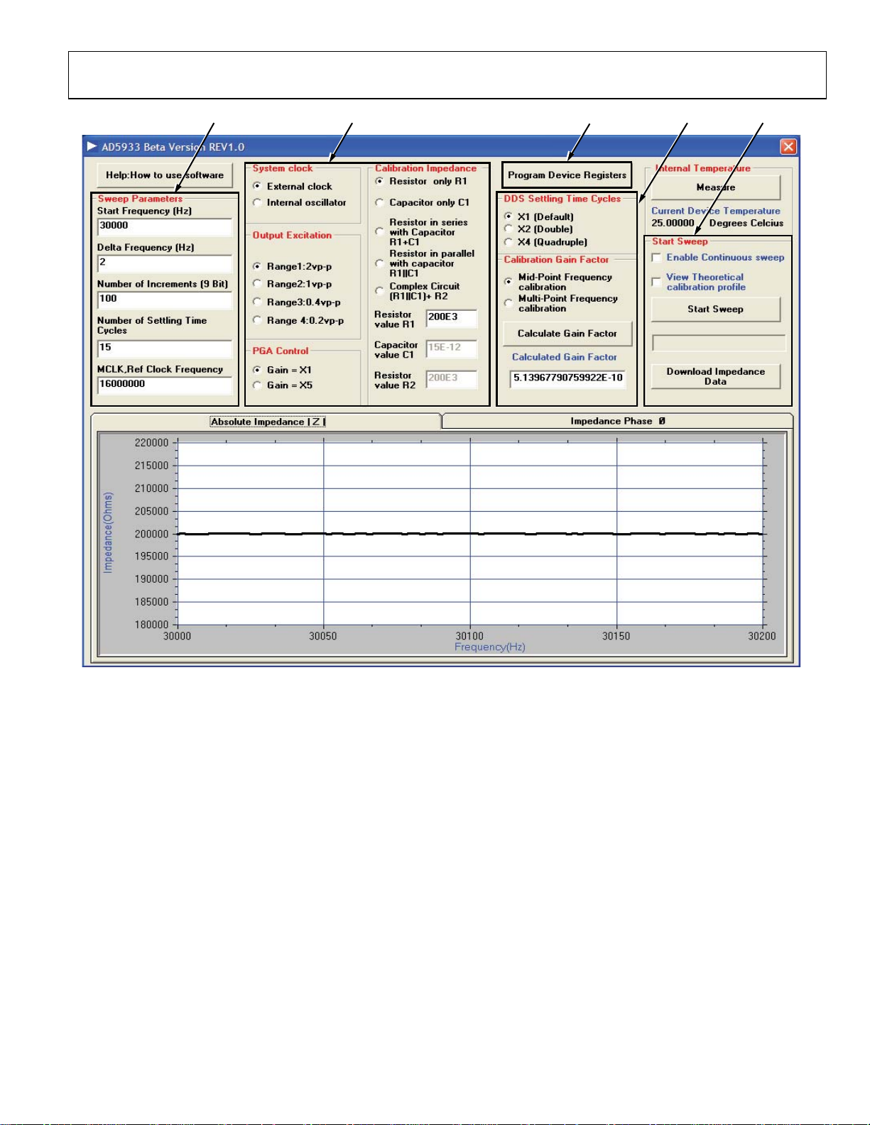
The sequence for performing a linear frequency sweep across a
200 k resistive impedance connected across the VOUT and
VIN pins within the frequency range of 30 kHz to 30.2 kHz is
outlined in this section. The default software settings for the
evaluation board are shown in Figure 12. (Note that a 200 k
resistor must be connected across the VIN and VOUT pins of
the AD5933). The default link positions are outlined in Tabl e 1,
see this before continuing.
To open the software, go to Start > Programs > Analog Devices >
AD5933 and click AD5933 Evaluation Software.
Figure 12 shows the graphic user interface program open and
running successfully. It also shows the interface panel along with
a frequency sweep impedance profile for a 200 k resistive
impedance (note R
To setup a typical sweep across a 200 k impedance (R
use the following steps:
• Set Start Frequency (Hz) to 30000 (Hz) within the Sweep
Parameters section (see 1 in Figure 12). The start frequency
is 24-bit accurate.
• Set Delta Frequency (Hz) to 2 (Hz) within the Sweep
Parameters section (see 1 in Figure 12). The frequency step
size is also 24-bit accurate.
• Set Number Increments (9 Bit) within the Sweep Parameters
section to 200 (see 1 in Figure 12) to set the number of
increments along the sweep to 200. The maximum number
of increments that the device can sweep across is 511, and
the value is stored in a register as a 9-bit value.
• Set Number of Settling Time Cycles to 15 (see 1 in Figure 12).
Note that when sweeping across a high-Q structure, such
as resonant impedance, users must ensure that the contents
of the settling time cycles register is sufficient to ensure
that the impedance under test settles before incrementing
between each successive frequency in the programmed
sweep. This is achieved by increasing the Number of
Settling Time Cycles value.
The delay between the time a frequency increment takes place
on the output of the internal direct digital synthesizer (DDS)
core and the time the ADC samples the response signal at
this new frequency is determined by the contents of the
number of settling time cycles registers (Register 0x8A and
Register 0x8B), see the AD5933 data sheet for further details.
For example, if a value of 15 is programmed into the Number
of Settling Time Cycles box, and if the next output frequency
is 32 kHz, the delay between the time the DDS core starts
to output the 32 kHz signal and the time the ADC samples the
response signal is 15 × (1/32 kHz) ≈ 468.7 µs. The maximum
number of settling time cycle delays that can be programmed
to the board is 511 cycles. The value is stored in a register as
a 9-bit value, and this value can be further multiplied by a
factor of 2 or by a factor of 4.
= 200 k).
FB
= 200 k),
FB
Evaluation Board User Guide UG-364
432 51
Figure 12. AD5933 Evaluation Software Front Panel (Impedance Profile of 200 kΩ Resistor Displayed)
• Choose the external clock as the system clock. Select
External clock in the System Clock section (see 2 in
Figure 12).
• Set Output Excitation voltage range of the AD5933 at
Pin 6 (VOUT) to Range1:2v p-p (see 2 in Figure 12). The
four possible output ranges available are 2 V p-p, 1 V p-p,
0.4 V p-p, or 0.2 V p-p, typically.
• Set the PGA gain of the ADC on the receive stage (either
×1 or ×5) in the PGA Control section to ×1 (see 2 in
Figure 12).
• Refer to the Calibration Impedance panel (see 2 in Figure 12).
Prior to making any measurements, calibrate the AD5933
with a known (that is, accurately measured) calibration
impedance connected between the VIN and VOUT pins of
the AD5933. The choice of calibration impedance topology
(for example, R1 in series with C1, R1 in parallel with C1)
depends on the application in question. However, ensure
that each component of the measured calibration impedance
is entered correctly into each chosen topology component
text box (see 2 in Figure 12). For this example, Resistor
Rev. 0 | Page 7 of 28
only R1 was chosen in the Calibration Impedance
section, that is, to measure the impedance of a 200 k
resistive impedance across frequency. Also for this example,
set Resistor value R1 to 200E3 (Ω).
• Click Program Device Registers (see 3 in Figure 12) to
program the sweep parameters as previously chosen into
the appropriate on-board registers of the AD5933 through
2
the I
C interface.
• The value programmed into the settling time cycles can be
further multiplied by a factor of 2 or a factor of 4 for a sweep.
Select ×1 (Default) in the DDS Settling Time Cycles section.
• Now that the frequency sweep parameters and gain settings
are programmed, the next step is to calibrate the AD5933
system by calculating the gain factor.
The explanation of the system calibration gain factor, a term
calculated once at system calibration, is provided in detail
in the AD5933 data sheet. The AD5933 gain factor must be
calibrated correctly for a particular impedance range before
any subsequent valid impedance measurement (refer to the
AD5933 data sheet for further details).
10441-013
UG-364 Evaluation Board User Guide
• To automatically calculate the gain factor(s) for the
subsequent sweep, click Calculate Gain Factor. The
evaluation software evaluates either a single midpoint
frequency gain factor or multipoint frequency gain factors,
that is, a gain factor for each point in the programmed sweep
(see 4 in Figure 12). The midpoint gain factor is determined
at the midpoint of the programmed sweep, and the multipoint
gain factors are determined at each point in the programmed
frequency sweep.
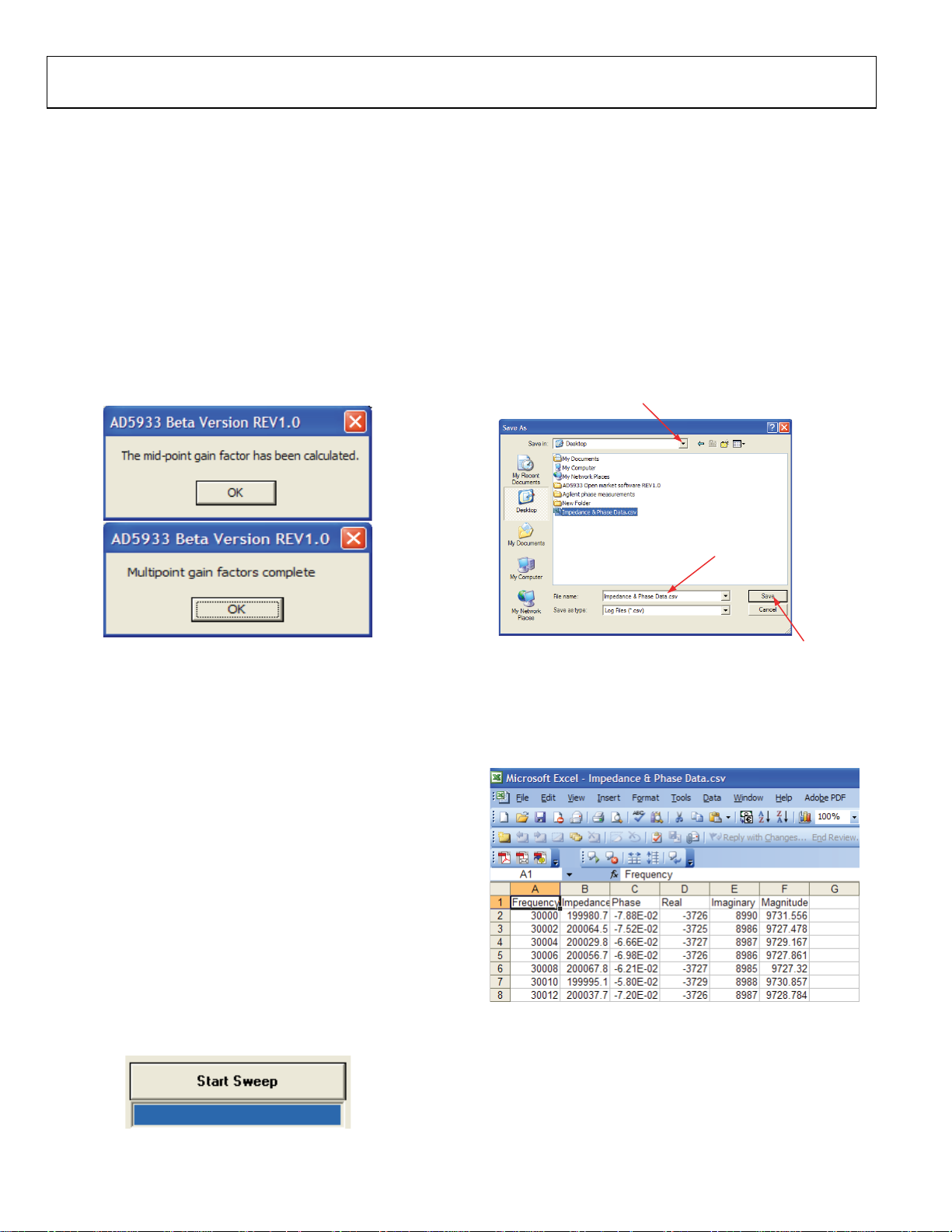
When either the midpoint gain factor or the multipoint gain
factors are calculated, a message appears on the evaluation
board software front panel, as shown in Figure 13. The gain
factor(s) returned to the evaluation software are subsequently
used for the sweep across the impedance under test.
• Click Measure in the Internal Temperature section of the
evaluation board software front panel to take a reading
from the on-board temperature sensor. This returns the
13-bit temperature of the device. See AD5933 data sheet
for more information on the temperature sensor.
• Click Download Impedance Data to download the frequency
sweep data (that is, frequency, impedance phase, real,
imaginary, and magnitude data) from the DFT of the sweep
(see 5 in Figure 12). The common dialog front panel is
presented as shown in Figure 15. Choose a file name in a
directory of choice and click Save (see Figure 15). This
saves the sweep data to a comma separated variable file
(.CSV) located in the chosen directory.
1. CHOOSE
DIRECTORY
2. CHOOSE
FILE NAME
10441-014
Figure 13. Confirmation of a Midpoint Calculation or
a Multipoint Gain Factors Calculation
After the system interface software calculates the gain factor(s)
for the programmed sweep parameters, the results are shown
in the Calculated Gain Factor box.
Note that should any of the system gain settings (for example,
change in output excitation range or PGA gain) change after
the system is calibrated (that is, gain factor(s) are calculated),
it is necessary to recalculate the gain factor(s) to subsequently
measure accurate impedance results. The gain factor(s)
calculated in the software are not programmed into the
AD5933 RAM and are only valid when the evaluation
software program is open and running. The gain factor(s)
are not retained in the evaluation software when the software
program is closed.
• Click Start Sweep (see 5 in Figure 12) to begin the sweep.
Once the evaluation software completes the sweep, it
automatically returns both a plot of the impedance vs.
frequency and phase vs. frequency for the impedance
under test (see Figure 12).The progress of the sweep is
outlined with a progress bar, as shown in Figure 14.
10441-015
Figure 14. Sweep Progress Bar (Blue)
3. SAVE THE FILE
Figure 15. Saving the Sweep Data
The contents of this file can be accessed by using Notepad
or Microsoft Excel to plot the data. Each file contains a single
column of data. The format of the downloaded data is shown
in Figure 16.
Figure 16. Opening the Sweep Data in Excel
10441-016
10441-017
Rev. 0 | Page 8 of 28
Evaluation Board User Guide UG-364
Each data entry corresponds to a single measurement
(frequency) point; therefore, if the value for the number of
increments is programmed as 511 point, the array contains
a single column of data with 512 data points, starting at the
start frequency and ending at stop frequency value, which
is determined by
Start Frequency + (Number of Increments × Delta
Frequency)
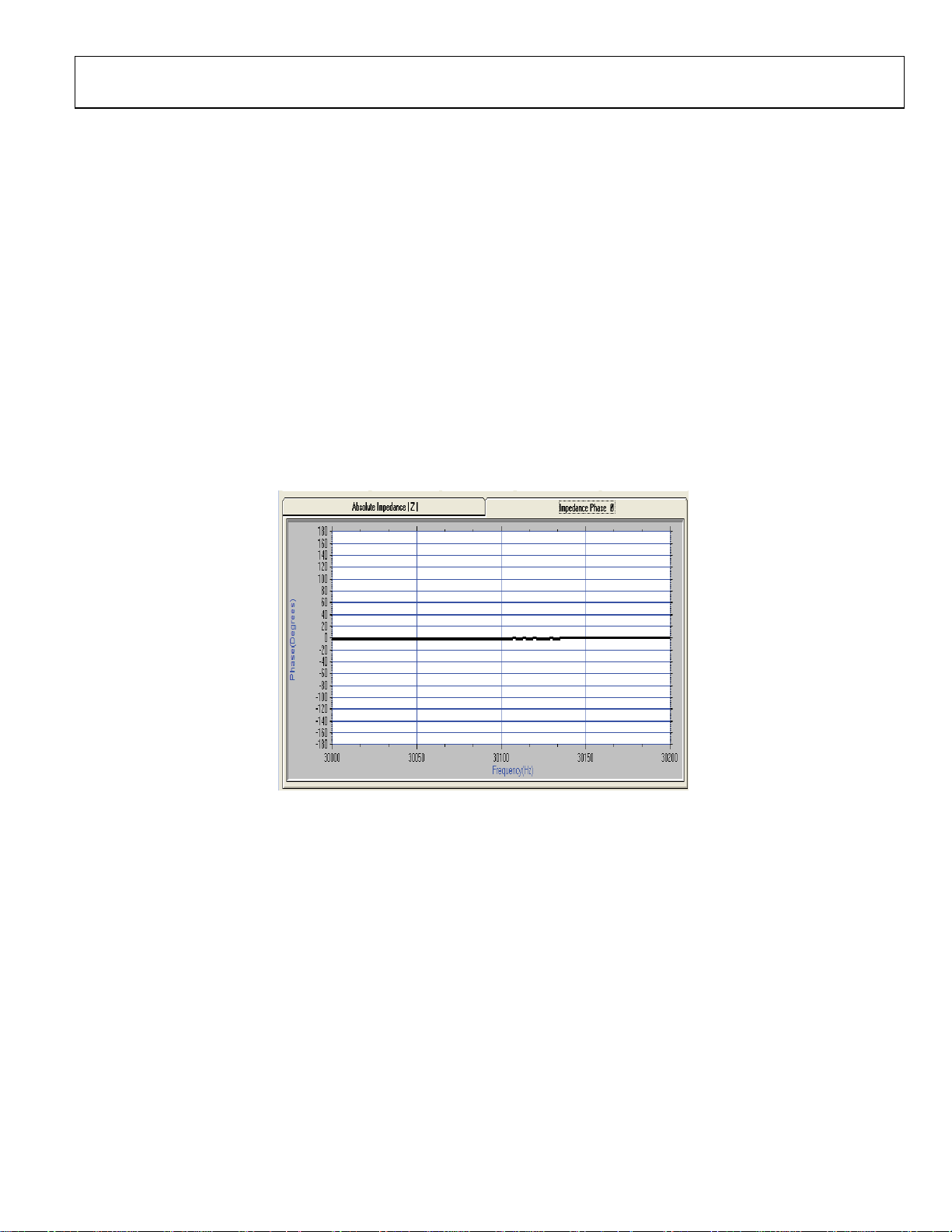
The impedance profile and phase profile vs. frequency appears
in the evaluation software front panel after the sweep has
completed. Click the individual tabs to switch between
Absolute Impedance |Z| and Impedance Phase Ø. Click
Absolute Impedance |Z| to show how the impedance under
analysis (Z
) varies across the programmed frequency
UNKNOWN
range. To view how the phase across the network under
analysis varies, click Impedance Phase Ø, as shown
in Figure 17.
Note that the phase measured by the AD5933 takes into
account the phase introduced through the entire signal path,
that is, the phase introduced through the output amplifiers,
receive current-to-voltage (I-V) amplifier, and the low-pass
filter, along with the phase through the impedance (Z
analysis connected between VOUT and VIN (Pin 6 and Pin 5
of the AD5933). Calibrate out the phase of the system using
a resistor before any subsequent impedance (Z
) phase
Ø
measurement is calculated. Calibrate with a resistor in the
evaluation software to calibrate the system phase correctly
(refer to the Impedance Measurement Tips section for
further details).
) under
Ø
10441-018
Figure 17. The Phase Tab on the A D5933 Evaluation Software Front Panel, Phase of 200 kΩ Resistor (0°) Displayed
Rev. 0 | Page 9 of 28
 Loading...