ANALOG DEVICES UG-349 Service Manual

EVAL-AD5222SDZ User Guide
UG-349
EVAL-AD5222SDZ
SYSTEM DEMONSTRATION
PLATFORM
10367-001
One Technology Way • P. O. Box 9106 • Norwood, MA 02062-9106, U.S.A. • Tel: 781.329.4700 • Fax: 781.461.3113 • www.analog.com
Evaluation Board for the AD5222 Digital Potentiometer
FEATURES
Full featured evaluation board for the AD5222
Various test circuits
Various ac and dc input signals
PC control via a separately purchased system demonstration
platform (SDP-B)
PC software for control
PACKAGE CONTENTS
EVAL-AD5222SDZ board
CD that includes
Self-installing software that allows users to control the
board and exercise all functions of the device
Electronic version of the AD5222 data sheet
Electronic version of the UG-349 user guide
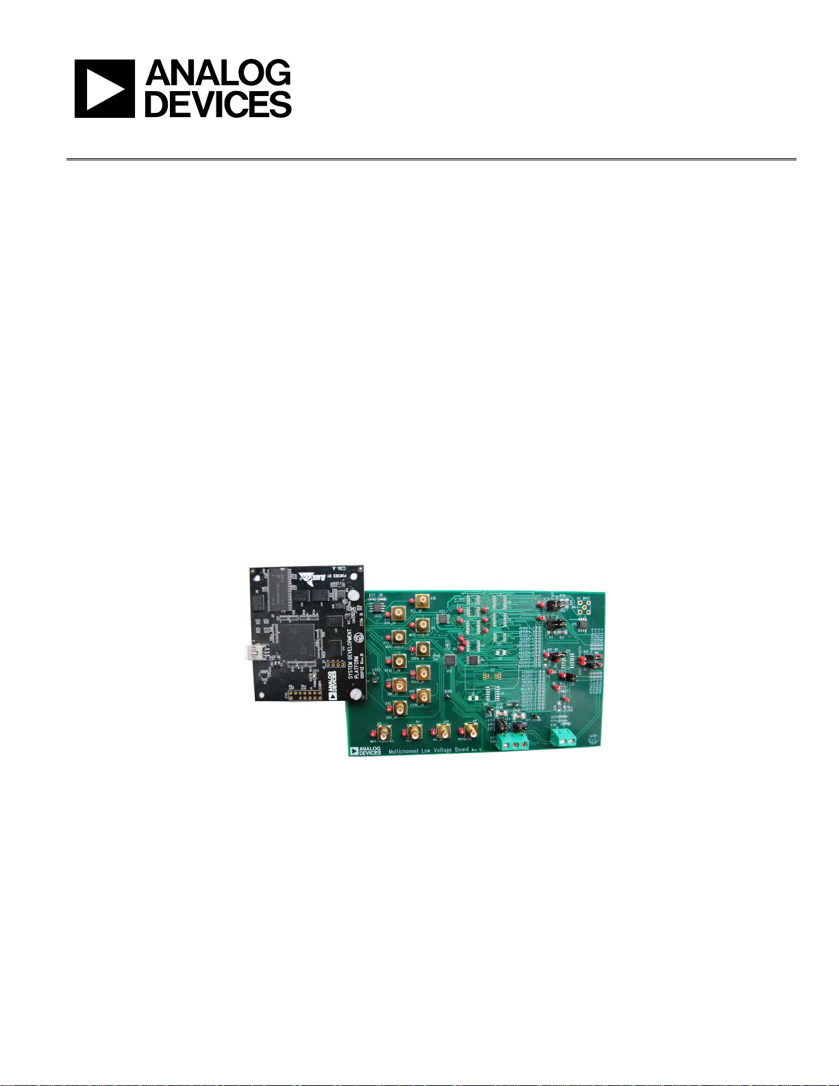
DIGITAL PICTURE OF EVALUATION BOARD WITH SYSTEM DEMONSTRATION PLATFORM
GENERAL DESCRIPTION
This user guide describes the evaluation board for evaluating
the AD5222—a dual-channel, 128-position, digital potentiometer
The AD5222 supports single-supply 2.7 V to 5.5 V operation,
making the device suited for battery-powered applications and
many other applications while offering a 0.2% channel-tochannel matching tolerance.
In addition, the AD5222 uses a high speed up/down interface,
allowing speeds of up to 15 MHz.
The EVA L-AD5222SDZ can operate in single-supply mode and
incorporates an internal power supply from the USB.
Complete specifications for the AD5222 part can be found in
the AD5222 data sheet, which is available from Analog Devices,
Inc., and should be consulted in conjunction with this user
guide when using the evaluation board.
PLEASE SEE THE LAST PAGE FOR AN IMPORTANT
WARNING AND LEGAL TERMS AND CONDITI ONS.
Figure 1.
Rev. 0 | Page 1 of 16

UG-349 EVAL-AD5222SDZ User Guide
TABLE OF CONTENTS
Features .............................................................................................. 1
Package Contents .............................................................................. 1
General Description ......................................................................... 1
Digital Picture of Evaluation Board with System
Demonstration Platform.................................................................. 1
Revision History ............................................................................... 2
Evaluation Board Hardware ............................................................ 3
Power Supplies .............................................................................. 3
Link Options ................................................................................. 3
REVISION HISTORY
12/11—Revision 0: Initial Version
Test Circuits ...................................................................................4
Evaluation Board Software ...............................................................6
Installing the Software ..................................................................6
Running the Software ...................................................................6
Software Operation .......................................................................6
Evaluation Board Schematics and Artwork ...................................7
Ordering Information .................................................................... 13
Bill of Materials ........................................................................... 13
Related Links ................................................................................... 14
Rev. 0 | Page 2 of 16

EVAL-AD5222SDZ User Guide UG-349
5 V (from SDP-B).
A24
VSS
This link should be connected to GND (analog ground).
EVALUATION BOARD HARDWARE
POWER SUPPLIES
The EVA L-AD5222SDZ supports using single power supplies.
The evaluation board can be powered either from the SDP port
or externally by the J1-1 and J1-2 connectors, as described in
Tabl e 1.
All supplies are decoupled to ground using 10 µF tantalum and
0.1 µF ceramic capacitors.
Table 1. Maximum and Minimum Voltages of the Connectors
Connector No. Label Voltage
J1-1 EXT Analog positive power supply, VDD.
VDD
J1-2 GND Analog ground.
Table 3. Link Functions
Link No. Power Supply Options
A25 VDD This link selects one of the following as the positive power supply:
For single-supply operation, it is 2.7 V
to 5 V.
LINK OPTIONS
Several link and switch options are incorporated in the
evaluation board and should be set up before using the board.
Tabl e 2 describes the positions of the links to control the
evaluation board by a PC, via the SDP-B board, using the
EVA L-AD5222SDZ in single-supply mode. The functions of
these link options are described in detail in Table 3 through
Tabl e 6.
Table 2. Link Options Setup for SDP-B Control (Default)
Link No. Option
A25 3.3 V
A24 GND
3.3 V (from SDP-B).
EXT (external supply from the J1-1 connector).
Rev. 0 | Page 3 of 16

UG-349 EVAL-AD5222SDZ User Guide
A
V
V
TEST CIRCUITS
The EVAL-AD5222SDZ incorporates several test circuits to
evaluate the AD5222 performance.
DAC
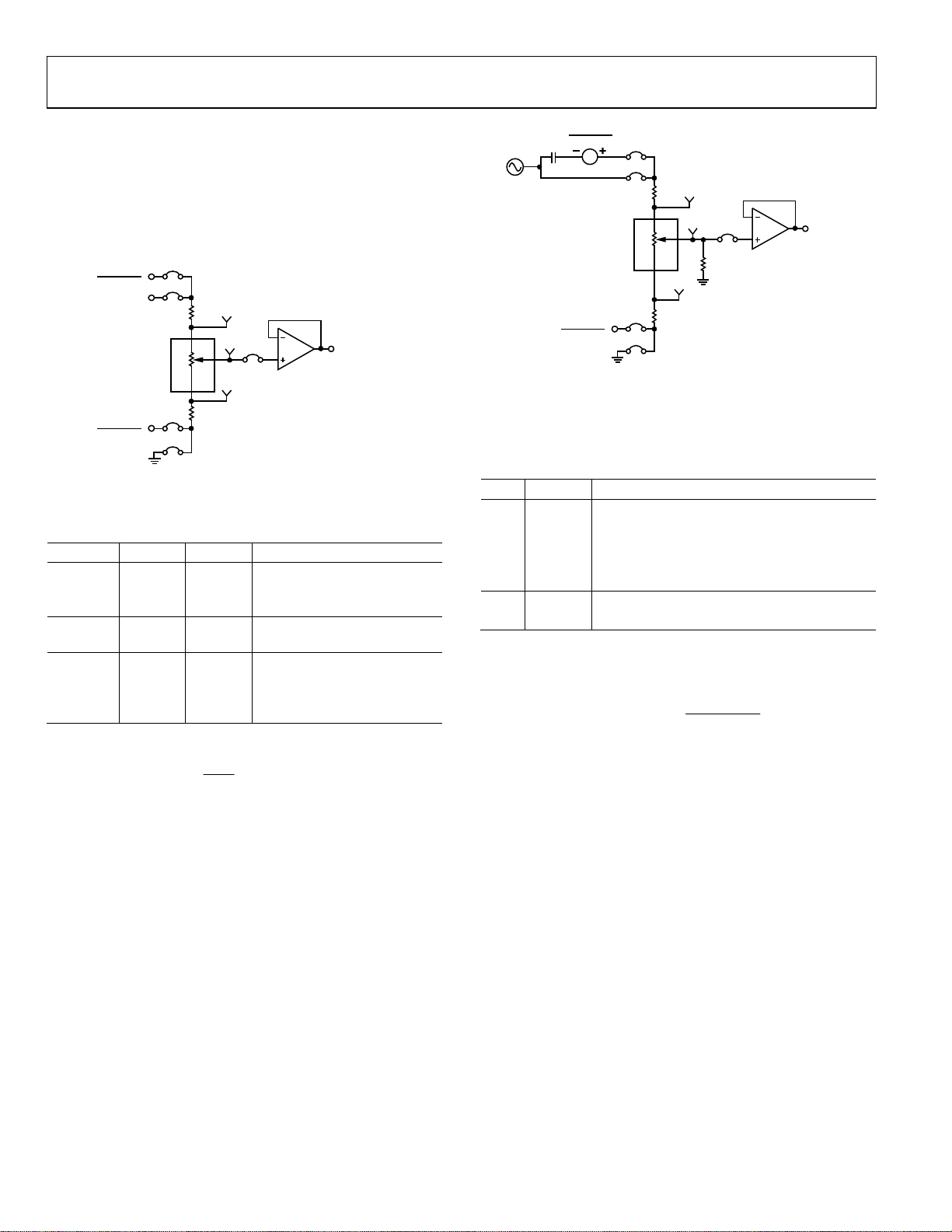
RDAC1 can be operated as a digital-to-analog converter (DAC),
as shown in Figure 2.
– V
2
– V
2
AC + DC
SS
VDD
V
DD
RDAC1
DC
SS
GND
A1
R34
W1
R35
W1
BUF_W1
B1
W1_BUF
10367-002
A1
B1
Figure 2. DAC
Connects Terminal A1 to
(VDD − VSS)/2
Connects Terminal W1 to an
output buffer
Connects Terminal B1 to
(VDD − VSS)/2
Connects Terminal B1 to
analog ground
R
WB1
VVV
)(
B1
A1
(1)
128
and VB1 in Equation 1.
A1
V
DD
V
DD
Table 4 shows the options available for the voltage references.
Table 4. DAC Voltage References
Terminal Link Options Description
A1 A20 AC + DC
VDD Connects Terminal A1 to VDD
W1 BUF_W1
B1 A21 DC
GND
The output voltage is defined in Equation 1.
OUT
where:
R
is the resistor between the W1 and B1 terminals.
WB1
V
is the voltage applied to the A1 terminal (A20 link).
A1
V
is the voltage applied to the B1 terminal (A21 link).
B1
However, by using the R34 and R35 external resistors, the user
can reduce the voltage of the voltage references. In this case, use
the A1 and B1 test points to measure the voltage applied to the
A1 and B1 terminals and recalculate V
AC Signal Attenuation
RDAC1 can be used to attenuate an ac signal, which must be
provided externally using the AC_INPUT connector, as shown
in Figure 3.
–
DD
SS
2
C_INPUT
1µF
V
DD
– V
2
SS
AC + DC
AC
RDAC1
DC
GND
A1
R34
W1
R35
W1
BUF_W1
R36
B1
W1_BUF
A1
B1
Figure 3. AC Signal Attenuator
Depending on the voltage supply rails and the dc offset voltage
of the ac signal, various configurations can be used as described
in Table 5.
Table 5. AC Signal Attenuation Link Options
Link Options Conditions
A20 AC + DC No dc offset voltage.
AC signal is outside the voltage supply rails
due to the dc offset voltage.
DC offset voltage ≠ VDD/2.1
AC All other conditions.
A21 DC Use in conjunction with ac + dc link.
GND All other conditions.
1
Recommended to ensure optimal total harmonic distortion (THD) performance.
The signal attenuation is defined in Equation 2.
nAttenuatio log20)dB( (2)
R
RR
WWB1
ENDTOEND
where:
is the resistor between the W1 and B1 terminals.
R
WB1
R
is the wiper resistance.
W
R
END-TO-END
is the end-to-end resistance value.
In addition, R36 can be used to achieve a pseudologarithmic
attenuation. To do so, adjust the R36 resistor until a desirable
transfer function is found.
10367-003
Rev. 0 | Page 4 of 16

EVAL-AD5222SDZ User Guide UG-349
R38
R
G
WB2
+=1
V
IN
RDAC2
B2
R42
W2
B2
W2
V
OUT
OAVOUT
C1
10nF
R41
1.7kΩ
R38
2.7kΩ
10367-004
R
V
IN
RDAC2
B2A2
R42
W2
B2
W2
V
OUT
OAVOUT
A2
C1
10nF
R41
1.7kΩ
R43
10367-005
R38
R
G
WB2
−=
V
IN
RDAC2
B2
R42
W2
B2
W2
V
OUT
OAVOUT
C1
10nF
R41
1.7kΩ
R38
2.7kΩ
10367-006
A30
NON-INVERTING
A30
INVERTING
Signal Amplifier
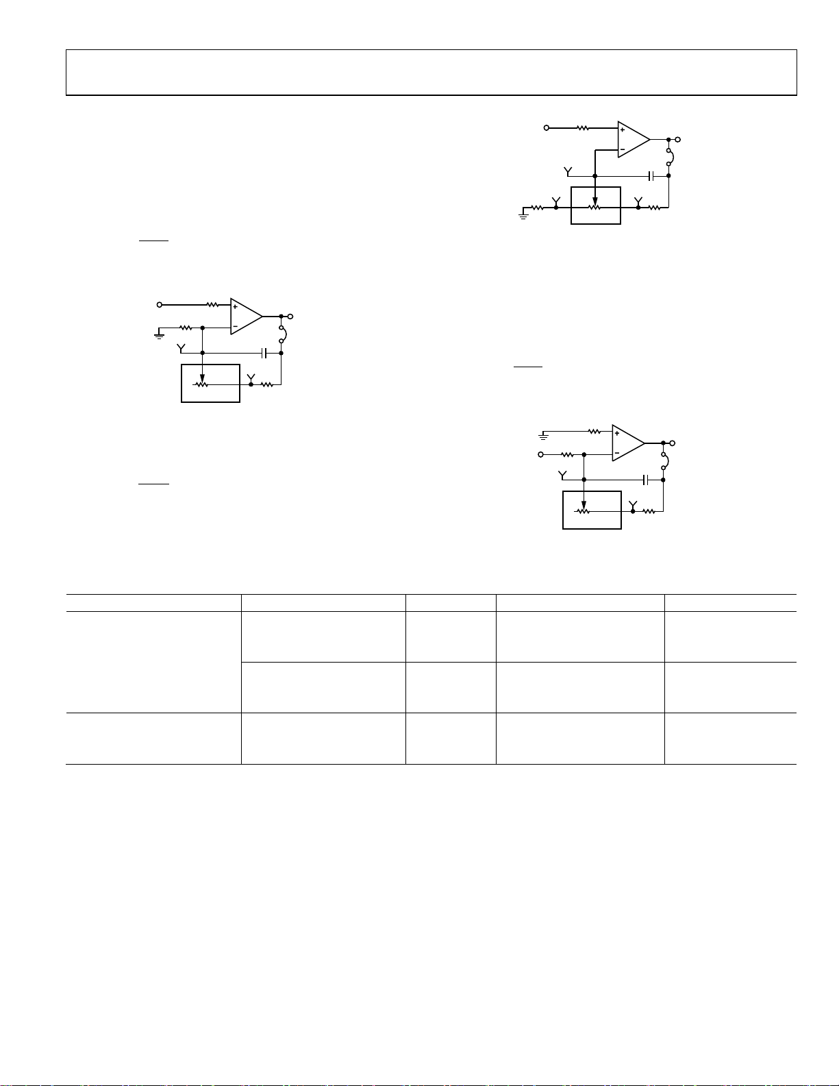
RDAC2 can be operated as an inverting or noninverting signal
amplifier supporting linear or pseudologarithmic gains. Table 6
shows the available configurations.
The noninverting amplifier with linear gain is shown in Figure 4,
and the gain is defined in Equation 3.
(3)
where R
is the resistor between the W2 and B2 terminals.
WB2
Figure 5. Pseudologarithmic Noninverting Amplifier
R43 and R42 can be used to set the maximum and minimum
gain limits.
The inverting amplifier with linear gain is shown in Figure 6,
and the gain is defined in Equation 5.
Note that the input signal, V
, must be negative.
IN
(5)
where R
is the resistor between the W2 and B2 terminals.
WB2
Figure 4. Linear Noninverting Amplifier
The noninverting amplifier with pseudologarithmic gain is
shown in Figure 5, and the gain is defined in Equation 4.
WB2
G +=1
(4)
R
AW2
where:
R
is the resistor between the W2 and B2 terminals.
WB2
R
is the resistor between the A2 and W2 terminals.
AW 2
Figure 6. Linear Inverting Amplifier
Table 6. Amplifier Selection Link Options
Amplifier Gain Link Label1 VIN Range
Noninverting Linear A27 LINEAR 0 V to VDD
A29 NON-INVERTING
A30 NON-INVERTING
Pseudologarithmic A27 PSEUDOLOG 0 V to VDD
A29 NON-INVERTING
Inverting Linear A27 LINEAR −VDD to 0 V
A29 INVERTING
1
See Figure 14.
Rev. 0 | Page 5 of 16
 Loading...