Evaluation Board User Guide
One Technology Way • P. O . Box 9106 • Norwood, MA 02062-9106, U.S.A . • Te l: 781.329.4700 • Fax: 781.461.3113 • www.analog.com
UG-339
ADL5304 Evaluation Board User Guide
FEATURES
4-layer printed circuit board (PCB), 53 mm × 72 mm form factor
Resistor programmable log slope and intercept
Single-or dual-supply operation
Full two argument logarithmic computation
On-board precision 100 nA reference
Optimized for very fast response at all input currents
Overall bandwidth of >4 MHz for inputs >1 μA
Bandwidth: 25 kHz at input of 1 nA and 350 kHz at 10 nA
10 decades of input range: 1 pA to 10 mA
Law conformance: ±0.25 dB from 100 pA to 100 μA
Log ratio or fixed-intercept operation
On-board precision 1.5 V and 2.0 V voltage references
Adaptive photodiode (PD) bias for low dark current
Default log slope of 10 mV/dB at VLOG pin
GENERAL DESCRIPTION
This user guide refers to the ADL5304 evaluation board, which
allows users to connect the ADL5304 precision log amplifier to
current sources with simple SMA connections or, with modification of the default configuration, to mount a photodiode to the
INUM input for optical power level applications.
The ADL5304 evaluation board is laid out to minimize errors
due to leakage into the sensitive INUM and IDEN nodes
through driven guards.
Slope and logarithmic intercept are programmable through
on-chip resistors and can be further optimized for specific
applications using external resistors. Additional components
can be added to optimize filtering for specific applications.
Adaptive photodiode bias is available using the IMON output to
optimize photodiode response and dark current.
Full details about the part are available in the ADL5304 data sheet,
which should be consulted when using the ADL5304-EVALZ.
PLEASE SEE THE LAST PAGE FOR AN IMPORTANT
WARNING AND LEGAL TERMS AND CONDITIONS.
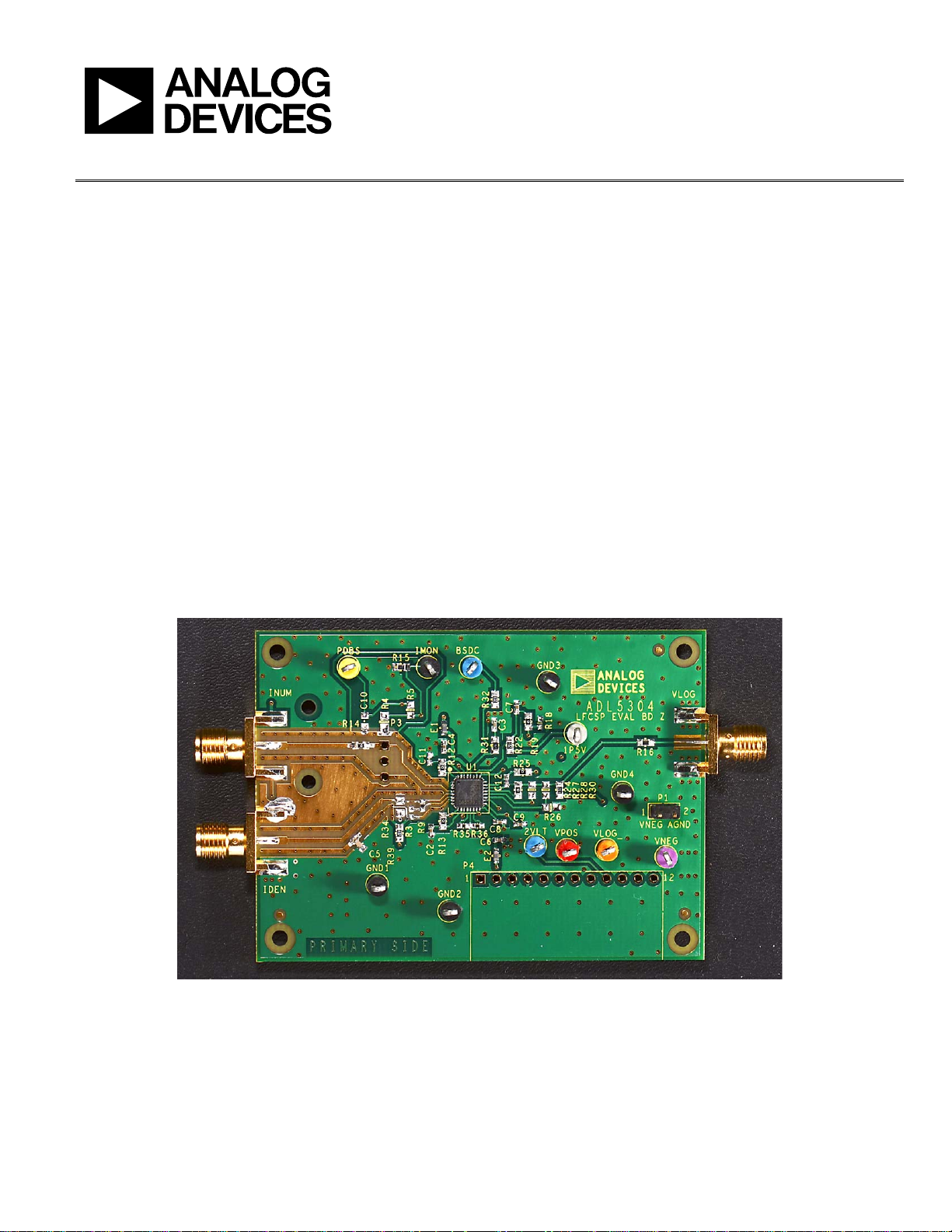
Figure 1. Top View of ADL5304 Evaluation Board
Rev. 0 | Page 1 of 16
10321-001

UG-339 Evaluation Board User Guide
TABLE OF CONTENTS
Features .............................................................................................. 1
General Description ......................................................................... 1
Revision History ............................................................................... 2
Evaluation Board Features ............................................................... 3
Power Supply ................................................................................. 3
Programming Slope and Intercept ............................................. 3
Photodiode Connections ............................................................. 3
1.5 V and 2.0 V References .......................................................... 3
IREF Fixed Current Reference .................................................... 3
Shields and Guards ....................................................................... 4
Stray Magnetic Fields ................................................................... 4
Logarithmic Ratio Operation ..................................................... 4
Voltage Source Operation ........................................................... 5
REVISION HISTORY
11/11—Revision 0: Initial Version
Speed and Filtering .......................................................................5
Guard Configurations .......................................................................6
Slope/Intercept Options ....................................................................7
External Connectors .........................................................................8
Analog I/O Connector, P4 ...........................................................8
INUM, IDEN, and VLOG SMA Connectors ............................8
Output Loading .............................................................................8
Single-/Dual-Supply Jumper, P1 .................................................8
Evaluation Board Schematics and Artwork ...................................9
Evaluation Board Optional Components .................................... 11
Ordering Information .................................................................... 12
Bill of Materials ........................................................................... 12
Related Links ............................................................................... 12
Rev. 0 | Page 2 of 16

Evaluation Board User Guide UG-339
EVALUATION BOARD FEATURES
POWER SUPPLY
The ADL5304 evaluation board can be powered from a single 5 V
supply for specified inputs from 1 pA to 3 mA. In single-supply
configuration, the VNEG bus is connected to ground using
Jumper P1. This is the default configuration of the board. In
single-supply operation, the V
the range of the VLOG output swing is 0.5 V to 2.5 V. Ground
referenced V
operation is not allowed in single-supply
SUM
configuration. With Jumper P1 removed, the ADL5304
evaluation board can be used in dual-supply mode. In dualsupply mode operation, the VNEG supply is connected to a
−2 V to −5 V source. This increases the specified input range
from 1 pA to 10 mA. The ADL5304 evaluation board can be
configured to operate with V
swing from −1 V to +1 V when VNEG is less than −2 V.
PROGRAMMING SLOPE AND INTERCEPT
The ADL5304 provides precision trimmed internal resistors to
allow programming options for slope and intercept without the
need for external components. The internal resistors connected
to Pin SCL1 to Pin SCL3 are accessed by Resistors R24 to R28.
Table 1 shows the values for slope, intercept, and offset available
through programming using 0 Ω resistors in the R24 to R28
positions. Additional slope, intercept, and offset values can be
configured by using nonzero resistors; however, performance
may be affected by drift and tolerance of the external components.
The intercept can also be adjusted by using both the INUM and
IDEN inputs.
PHOTODIODE CONNECTIONS
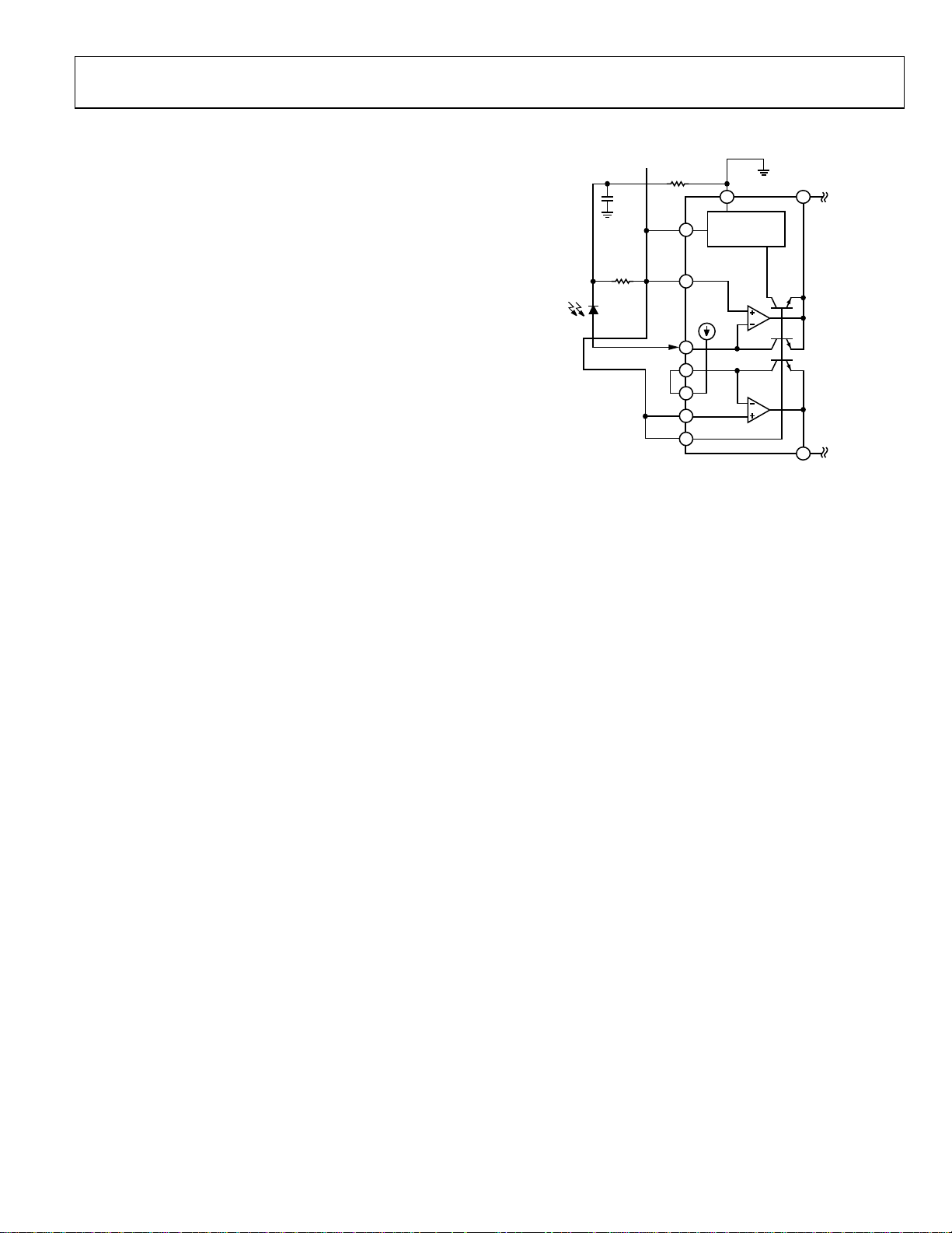
The ADL5304 evaluation board has a provision to connect a
p-intrinsic-n (PIN) photodiode to the INUM input at Connector
P3 (see Table 4). The monitor current output (I
easy configuration of an adaptive photodiode bias scheme. Input
current, I
the IMON pin of 1.1 × I
I
, the additional current must flow in an external resistor,
NUM
R4, equal to 10 × R
series resistance of the photodiode. This ensures that the actual
junction of the photodiode is biased as close as possible to 0 V
to minimize dark current. Capacitor C10 provides potential
filtering and dynamic currents during fast transients. The value
for best bias response depends on the photodiode used and
should be determined experimentally.
If the adaptive bias is not used, the IMON pin must be
connected to ground by populating R5 with a 0 Ω resistor.
, is multiplied to give an effective output current at
NUM
NUM
, where RS is the value of the internal parasitic
S
reference voltage is 1.5 V and
SUM
at ground and a V
SUM
LOG
) provides
MON
output
. Because the photodiode produces
FROM 1. 5V VREF
C10
R4
10*R
DIO
PD
SHIELD
SHIELD
Figure 2. Adaptive Photodiode Bias
VSM1
VSM2
INUM
IDEN
IREF
VSM3
VSM4
R5
0
2
3
4
5
6
7
8
30
MONITOR AND
PD BIAS
(1.1× I
1.5V
100nA
1.5V
NUM
Q1
Q2
VNUMIMON
)
Q3
VDEN
32
9
10321-002
1.5 V AND 2.0 V REFERENCES
Accurate 1.5 V (Pin 1P5V) and 2.0 V (Pin 2VLT) reference
outputs allow precise repositioning of the intercept using external resistors. These voltages are available on test points and on
the P4 connector (see Table 2). The 2.0 V reference can be used
in adaptive photodiode mode to set up a precise 0.5 V bias across
the photodiode. See the ADL5304 data sheet for more information. The 2.0 V reference can also be used to set a different
current reference for the IDEN input by removing R9 and
populating R3 and R34. The value of R34 is calculated based on
the V
V
voltage, R34 = (2.0 −V
SUM
= 1.5 V to generate an I
SUM
)/I
SUM
current of 1 A, R34 = 500 kΩ.
DEN
. For example, with
DEN
IREF FIXED CURRENT REFERENCE
The ADL5304 provides a fixed 100 nA reference (I
in the default configuration, is connected to the IDEN input for
single input log calculation. For applications requiring both
inputs to the logarithmic argument, IREF can be disconnected
from IDEN by removing Resistor R9 and applying current
directly to the IDEN input. When IREF is not used, it must be
connected to V
through Resistor R3 to dump the generated
SUM
100 nA current.
), which,
REF
Rev. 0 | Page 3 of 16

UG-339 Evaluation Board User Guide
SHIELDS AND GUARDS
Reducing errors from external sources in a current sensing
circuit requires a different approach from the voltage sensing
input of the typical high impedance op amp circuit. Leakage
can be a significant source of error for highly sensitive log amps,
especially at the low end of their range. For example, a 1 GΩ
leakage path to ground from the INUM input with V
the default 1.5 V generates a 1.5 nA offset. The ADL5304 evaluation board makes extensive use of guards to reduce the effects
of leakage at low input levels; however, it is still important to
carefully handle and clean the ADL5304 evaluation board to
prevent contaminants from handling or leakage currents from
improper washing of the PCB. A common mistake for those
unfamiliar with low level current sensing is to attach a high
impedance scope probe or meter to measure the input for debugging. This can cause significant error, because the typical 1 M ~
100 MΩ impedance of these probes sources/sinks current from
the input depending on their bias.
In instrumentation applications where measurements <1 nA are
required, the use of triaxial cables and connectors is common to
reduce leakage through the insulating dielectric by carrying a
continuous guard from current source to sensing circuit on the
intermediate conductor. This type of guarding circuit is different from a conventional electrostatic shield used in voltage sensing
applications. An electrostatic shield relies on low impedance
and the ability to flow current freely to minimize voltage induced
on the shield that can capacitively couple into a high impedance
input. A guard is actively driven to the same voltage as the
current-carrying center conductor, eliminating leakage through
the dielectric between the center conductor and the guard. The
guard does not flow current other than the leakage from the guard
to the outer shield and is usually only connected to a single end
of the cable, because any significant current flow through the
guard can couple inductively to the center conductor. Using the
ADL5304 evaluation board, the guard can be driven either from
the current source (see Figure 5) or from the ADL5304 (see
Figure 6).
The ADL5304 evaluation board can bias the shield of a coaxial
cable that is connected to the INUM input to the nominal V
voltage by removing Resistor R41 and populating Resistor R40,
but this requires careful consideration of the environment on
the other side of the cable. For example, if the ADL5304 evaluation board is configured for V
= 1.5 V, connecting the other
SUM
end of the INUM coaxial cable to an instrument with a ground
referenced shield pulls V
to ground and collapses the input
SUM
stage of the ADL5304. Floating the current source end of the
shield provides a low leakage guard, but a separate return path
for the signal current must then be provided (see Figure 7). If
cable dielectric leakage is not a concern, the INUM input can be
connected directly to a coaxial cable with the shield, providing
signal ground (see Figure 8).
SUM
set to
SUM
STRAY MAGNETIC FIELDS
Current input devices such as the ADL5304 are sensitive to their
environments in ways that are not typically a problem with high
impedance input devices like voltage input op amps, particularly
in high bandwidth applications where filtering is not an option.
Because of its excellent sensitivity and low noise, the ADL5304
is capable of operation at currents easily influenced by stray
magnetic fields. This can lead to unwanted signals coupling into
the ADL5304 in unexpected ways. An example of this is shown
in Figure 3. In a typical circuit testing environment, eddy currents from instrument power supplies are contained in the steel
of the test cart. The low impedance of the cart prevents the eddy
currents from generating a sufficient voltage for electrostatic
coupling into the typical voltage sensing circuit. In a current
sensing application using the ADL5304, the loop currents in the
metal cart can inductively couple into the traces and cable used
to build the test circuit and into the INUM and IDEN inputs. In
this instance, shielding and guarding are ineffective at decoupling
the interferer and receiver circuits. The best ways to prevent this
type of coupling are careful design to minimize stray magnetic
fields, increasing the distance between the interferer and receiver
circuits, removing the coupling mechanism, in this example the
steel work surface, or using Mu-Metal or similar high magnetic
permeability material to provide a magnetic shield.
EDDY CURRENT S INDUCED BY STRAY MAGNETIC FIELDS
FUNCTION GENERATOR
SQUARE
SINE
1.000 kHZ
TRIANGLE
Sto/Rcl
POWER SUPPLY
INSULATING SILICONE PAD
STEEL WORK SURFACE
Figure 3. Inductive Coupling of Poorly Shielded Instrument Power Supplies
OSCILLOSCOPE
Output
1 2 3 4
LOGARITHMIC RATIO OPERATION
Log ratio operation of the ADL5304 is possible using both the
INUM and IDEN inputs. For log ratio operation, IREF must be
disconnected from IDEN by removing R9.
The value of V
I
and the programmed slope (R24/R28), offset by the INPS
DEN
depends on the log of the ratio of I
LOG
voltage (R18, R19) according to the following formula:
I
NUM
VV
log
Y
LOG
10
V
I
DEN
OFS
where:
denotes slope.
V
Y
V
denotes the voltage offset applied at the INPS pin (1.5 V in
OFS
the default configuration).
Because the ratio of I
unity, V
can be of either polarity, requiring a negative supply
LOG
NUM/IDEN
can be either greater or less than
in some cases. For example, if the ratio varies from 1:1000 to
1000:1 and a slope of 20 mV/dB is required, the peak swing is
±1.2 V around V
OFS
.
NUM
and
10321-003
Rev. 0 | Page 4 of 16

Evaluation Board User Guide UG-339
Option 5 in Table 1 provides this with an intercept, IZ, of 17.8 pA
(V
= 1.5 V) with V
OFS
results in 0.3 V ≤ V
The electrical characteristics of I
the exception of the I
I
signal and allows adaptive photodiode bias at the INUM
NUM
= ±1.2 V around V
LOG
≤ 2.7 V.
LOG
and I
NUM
current, which is derived from the
MON
= 1.5 V, which
OFS
are identical, with
DEN
input only.
VOLTAGE SOURCE OPERATION
In test situations where a precision current source is not available
or a dynamic signal is required, a voltage source or function
generator can be used to supply I
current through a resistor
NUM
in series with the INUM input. In the default configuration,
R14 is a 0 Ω, 0603 resistor. Due to the large input range of the
ADL5304, it is very difficult to find a voltage source with
sufficient range to fully exercise the ADL5304. This limitation
can be mitigated by using different resistor values to access
different segments of the ADL5304’s ra nge .
The INUM and IDEN inputs cannot source current. When
using a voltage source and series resistor to provide INUM or
IDEN current, the source voltage must always be positive
relative to the V
, the translinear device that performs the logarithmic
V
SUM
voltage. If the voltage source drops below
SUM
function saturates and the feedback amplifier rails as it attempts
to balance the loop around the translinear device. This will not
damage the ADL5304, but the recovery time of the input is
directly related to the input current and the capacitance seen by
the input. At low input currents, the input can take significantly
longer to recover from momentary transients that attempt to
source current.
SPEED AND FILTERING
Filtering to Improve Noise and Dynamic Behavior
The noise at the output of a log amp, particularly at low current
levels, leads to uncertainty in the measurement. Noise amplitude
is limited by the finite bandwidth. If measurement speed is not of
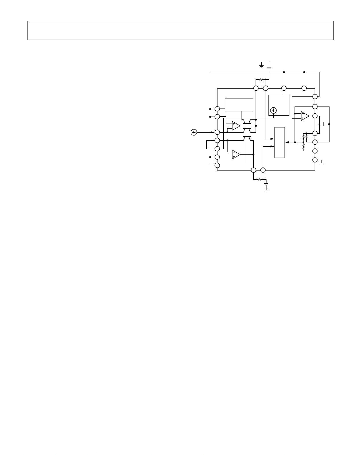
primary concern, additional filtering can reduce noise. Figure 4
shows the locations provided on the ADL5304 evaluation board
for additional external filtering.
Typically, capacitors are not used on the numerator side (I
to keep the speed of the device as high as possible. On the
denominator side (I
noise. In applications where I
logarithmic equation and I
), additional filtering is useful to reduce
DEN
is used as the reference to the
NUM
is a variable, for example, where a
DEN
NUM
)
reverse logarithmic slope is desired, filtering can be performed
on the numerator side (I
MONITO R AND
PD BIAS
(1.1× I
2
VSM1
VSM2
INUM
IDEN
IREF
VSM3
VSM4
1.5V
3
4
5
6
1.5V
7
8
Figure 4. Evaluation Board Filtering Locations
).
NUM
R12
VNUM INNM
32 31 26
)
NUM
V
NUM
V
9
VDEN INDN
10
R13
DEN
C2
C11
100nA
BIAS
TEMPERATURE
1P5V DCBI
1.5V
5kΩ 5kΩ
I
LOG
7.5kΩ
COMPENSATION
27
24
INPS
INMS
23
VLOG
22
CFB
21
SCL1
20
SCL2
19
SCL3
ACOM
18
A capacitor placed on the INUM and IDEN inputs effectively
reduces the bandwidth of the input stages. A few picofarads
of capacitance (<5 pF) reduce the bandwidth significantly for
currents below approximately 1 µA, and 1 nF to 10 nF are
normally enough to reduce the bandwidth up to the maximum
10 mA of input current. When measurement speed is of primary
importance, it is better to add filtering after the FET amp outputs,
in which case, C2 and R13 for the INDN inputs and C11 and R12
for the INNM inputs are the best locations. A bias current of
approximately 35 µA flows from the INNM and INDN pins
through Resistors R12 and R13, raising the voltage at the INNM
and INDN pins. To prevent this voltage rise from limiting headroom in the temperature compensation block, the value of R12
and R13 should not be much larger than 1 kΩ.
Adding a capacitor, C12, adds additional filtering at the buffer
output. This capacitor also helps to optimize the pulse response
by placing a zero across the feedback resistor (2.5 kΩ in the
default configuration). A good value to start with is 22 pF; this
introduces a zero at 2.9 MHz that can improve the pulse response
for input currents greater than 100 µA.
10321-004
Rev. 0 | Page 5 of 16
 Loading...