Evaluation Board User Guide
UG-336
One Technology Way • P. O . Box 9106 • Norwood, MA 02062-9106, U.S.A. • Tel : 781.329.4700 • Fax : 781.461.3113 • www.analog.com
Evaluating the ADP199 High-Side Load Switch
FEATURES
Ultrasmall, 0.8 mm × 0.8 mm, 4-ball, 0.4 mm pitch WLCSP
Low RDS
Low input voltage range of 0.9 V to 3.6 V
500 mA continuous operating current
Operating temperature range: T
of 40 mΩ
ON
= −40°C to +85°C
J
EVALUATION BOARD
GENERAL DESCRIPTION
The ADP199 evaluation board (ADP199CB-EVALZ) is
used to demonstrate the functionality of the ADP199
high-side load switch.
Simple device measurements such as V
(RDS
), ground current, and shutdown current can be dem-
ON
onstrated with only a single voltage source, a voltage meter, a
current meter, and a load resistor.
Complete information about the ADP199 high-side load
switch is available in the ADP199 data sheet, which should
be consulted when using the ADP199CB-EVALZ.
IN
to V
resistance
OUT
PLEASE SEE THE LAST PAGE FOR AN IMPORTANT
WARNING AND LEGAL TERMS AND CONDITIONS.
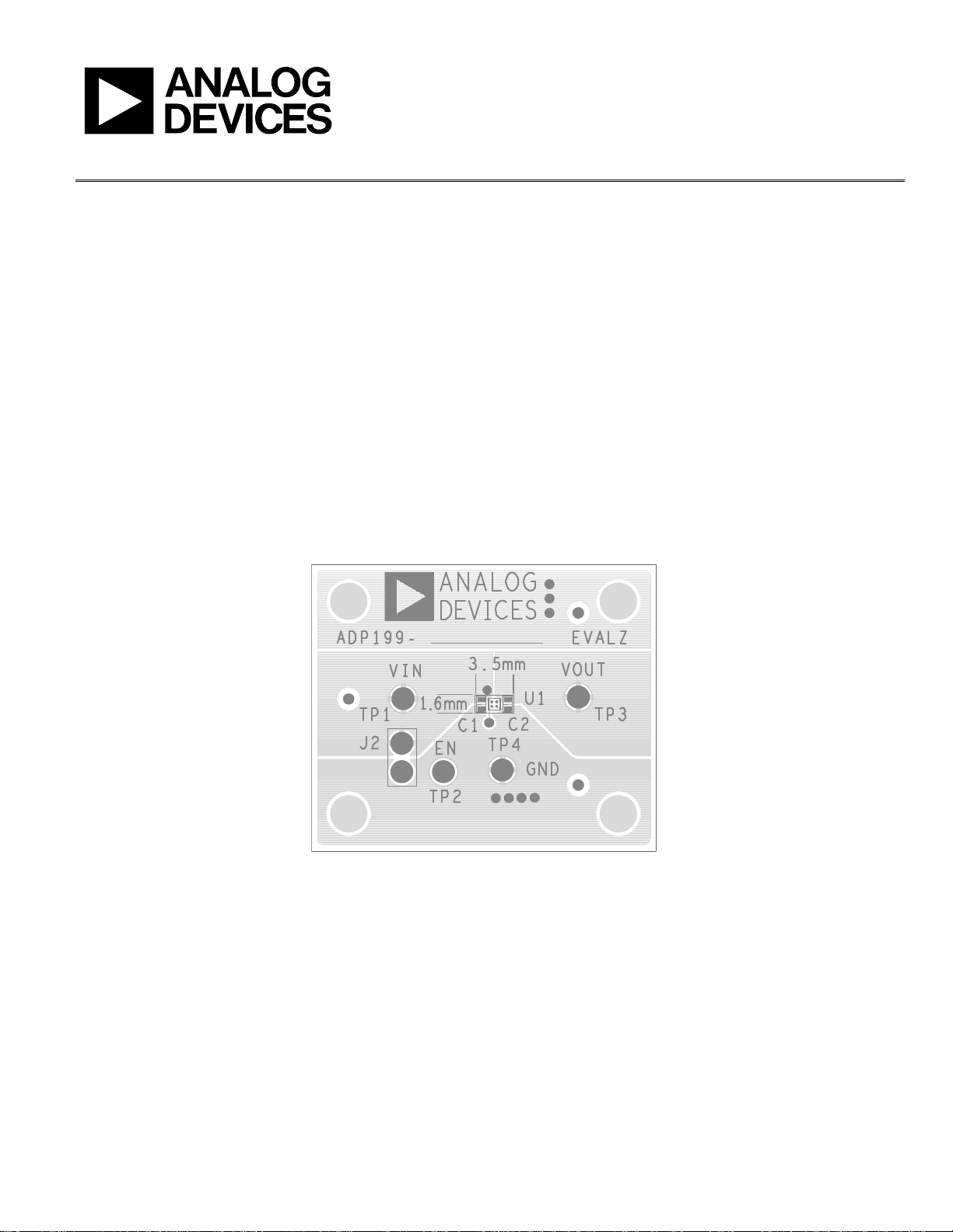
Figure 1.
Rev. 0 | Page 1 of 8
10294-001

UG-336 Evaluation Board User Guide
TABLE OF CONTENTS
Features .............................................................................................. 1
General Description ......................................................................... 1
Evaluation Board .............................................................................. 1
Revision History ............................................................................... 2
Evaluation Board Schematic and Hardware ................................. 3
VIN to V
Resistance (RDSON) Measurements ........................... 4
OUT
REVISION HISTORY
11/11—Revision 0: Initial Version
Ground Current Measurements ......................................................5
Ground Current Consumption ...................................................5
Shutdown Current Measurements ..................................................6
Ordering Information .......................................................................7
Bill of Materials ..............................................................................7
Rev. 0 | Page 2 of 8

Evaluation Board User Guide UG-336
EVALUATION BOARD SCHEMATIC AND HARDWARE
V
IN
+
C1
J2
VIN
EN
VOUT
U1
GND
V
OUT
+
C2
10294-002
Figure 2. Evaluation Board Schematic
Table 1. Evaluation Board Hardware Components
Component Function Description
U1 Load switch ADP199ACBZ-R7 high-side load switch.
C1 Input capacitor Input bypass capacitor, 0.1 μF. Optional to improve transient performance. Connect C1 from VIN to GND.
C2 Output capacitor Output capacitor, 0.1 μF. Optional to improve transient performance. Connect C2 from VOUT to GND.
J2 Jumper Jumper. Connects EN to VIN for automatic startup.
Rev. 0 | Page 3 of 8
 Loading...