Evaluation Board User Guide
UG-334
10272-001
ADP1876
GND
TERMINAL
VIN
TERMINAL
GND
TERMINAL
V
OUT1
TERMINAL
V
OUT2
TERMINAL
GND
TERMINAL
One Technology Way • P. O. Box 9106 • Norwood, MA 02062-9106, U.S.A. • Tel: 781.329.4700 • Fax: 781.461.3113 • www.analog.com
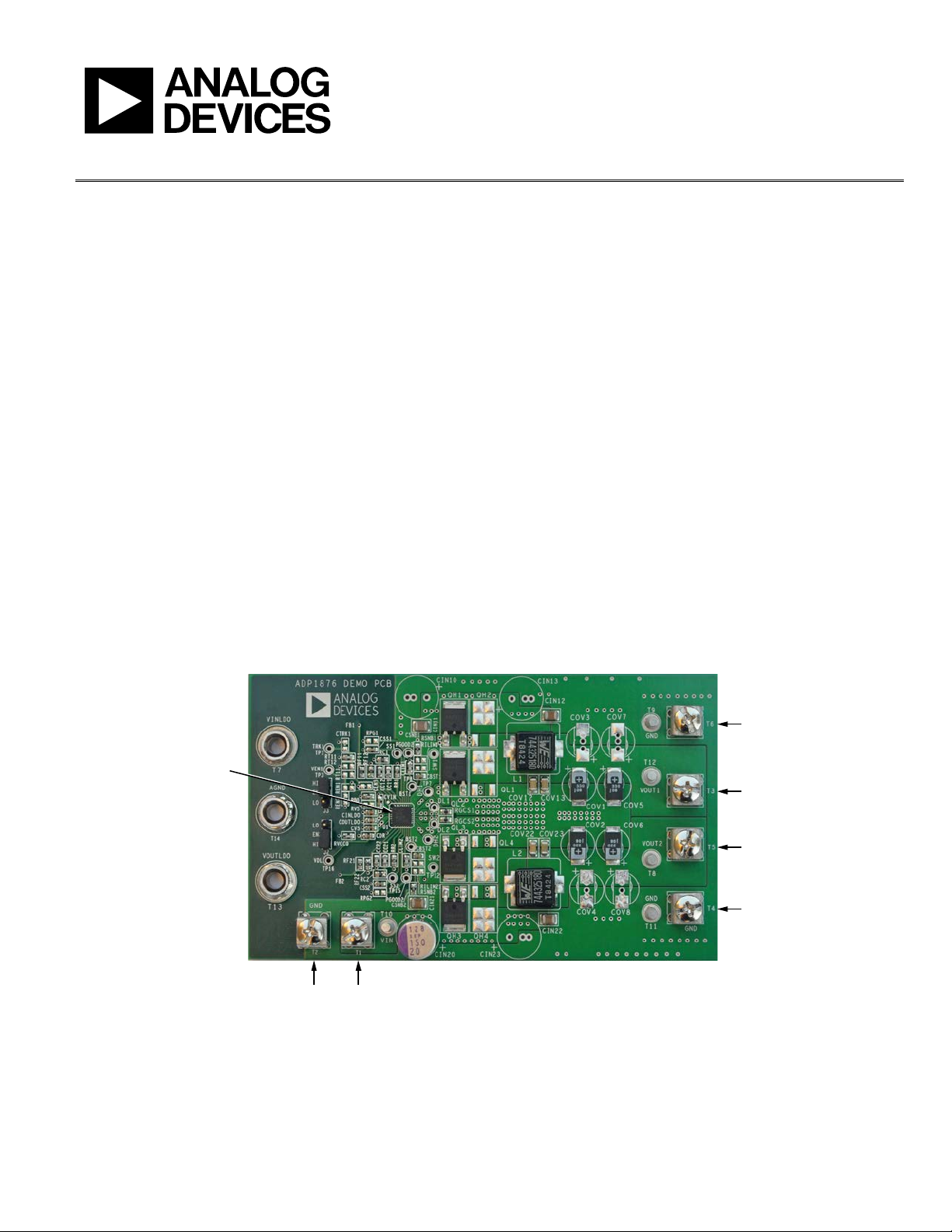
Evaluation Board for the ADP1876 Step-Down DC-to-DC Controller
FEATURES
Input range: 10 V to 20 V
Two output voltages: 5 V and 1.8 V
Output current: 13 A per channel
Switching frequency: 600 kHz
Operates in PWM
Compact, low cost, and efficient design
EVALUATION BOARD DESCRIPTION
This user guide describes the design, operation, and test results
of the ADP1876-E VA L Z . The input range for this evaluation
board is 10 V to 20 V, and the two regulated output voltages are
set to 5 V (V
current. The power components, such as the MOFSETS, inductors,
and bulk input and output capacitors, were chosen to yield a low
system cost and good efficiency.
) and 1.8 V (V
OUT1
) with a maximum 13 A output
OUT2
ADP1876-EVALZ EVALUATION BOARD
ADP1876 DEVICE DESCRIPTION
The ADP1876 is a dual-channel, step-down switching controller
with integrated drivers for external N-channel synchronous power
MOSFETs. The two PWM outputs are phase shifted 180°, which
reduces the input rms ripple current, thus minimizing the required
input capacitance.
In addition, boost diodes are integrated into the ADP1876,
which lowers the overall system cost and component count. The
ADP1876 is configured to operate in forced PWM continuous
conduction mode.
The ADP1876 includes externally adjustable soft start, output
overvoltage protection, externally adjustable current limit,
power good and tracking function for Channel 1. The ADP1876
provides an output voltage accuracy of ±0.85% for a −40°C to
+85°C junction temperature and ±1.5% for a −40°C to +125°C
junction temperature. This controller can be powered from a
2.75 V to 20 V supply and is available in a 32-lead, 5 mm × 5 mm
lead frame chip scale package (LFCSP).
PLEASE SEE THE LAST PAGE FOR AN IMPORTANT
WARNING AND LEGAL TERMS AND CONDITIONS.
Figure 1.
Rev. 0 | Page 1 of 16

UG-334 Evaluation Board User Guide
TABLE OF CONTENTS
Features .............................................................................................. 1
Evaluation Board Description......................................................... 1
ADP1876 Device Description ......................................................... 1
ADP1876-EVALZ Evaluation Board .............................................. 1
Revision History ............................................................................... 2
Component Design .......................................................................... 3
Inductor Selection ........................................................................ 3
Input Capacitors ........................................................................... 3
REVISION HISTORY
11/11—Revision 0: Initial Version
Output Capacitors .........................................................................3
MOSFET Selection ........................................................................3
Test Results .........................................................................................4
Evaluation Board Operating Instructions ......................................6
Evaluation Board PCB Layout .........................................................7
Evaluation Board Schematics and Artwork ...................................8
Ordering Information .................................................................... 12
Bill of Materials ........................................................................... 12
Rev. 0 | Page 2 of 16

Evaluation Board User Guide UG-334
COMPONENT DESIGN
For information about selecting power components and
calculating component values, see the ADP1876 data sheet.
INDUCTOR SELECTION
A 1.8 µH inductor with an 18 A saturation current rating
(744325180 from Würth Elektronik) is selected. This is a
compact inductor with a ferrite core, which offers high
performance in terms of low R
and low core loss.
DC
INPUT CAPACITORS
Because of the very low ESR and high input current rating of
multilayer ceramic capacitors (MLCCs), two 10 µF MLCCs in
Size 1210 are selected as the input capacitors at the input of each
channel. In addition, a 150 µF bulk OS-CON™ (aluminum solid
capacitor with conductive polymer) capacitor from SANYO is
chosen for filtering out unwanted low frequency noise from the
input power supply.
OUTPUT CAPACITORS
A combination of POSCAP™ polymer capacitors and MLCCs
are selected for the output rails. Polymer capacitors have low
ESR and high current ripple rating. Connecting polymer
capacitors and MLCCs in parallel is very effective in reducing
voltage ripple. Two 330 µF POSCAP capacitors and two 22 µF
MLCCs are selected for each output.
MOSFET SELECTION
For low output or low duty cycle, select a high-side MOSFET
with fast rise and fall times and with low input capacitance to
minimize charging and switching power loss. For the synchronous
rectifier (low-side MOSFET), select a MOSFET with low R
because the switching speed is not critical and there is no switching
power loss in the low-side MOSFET.
The MOSFET IPD050N03L in PG-TO252-3-11 (DPA K ) from
Infineon is chosen for both the high-side and low-side MOSFETs
for a balance between low cost and good efficiency. The R
the IPD050N03L is about 6 mΩ at a V
of 5 V.
GS
DSON
DSON
of
Rev. 0 | Page 3 of 16

UG-334 Evaluation Board User Guide
100
90
80
70
60
50
40
30
20
10
0
0 2 4 6 8 10 12 14
LOAD (A)
EFFICIENCY (%)
10272-002
V
OUT2
= 1.8V
T
A
= 25°C
V
IN
= 12V
V
OUT1
= 5V
0
–0.005
–0.010
–0.015
–0.020
–0.025
–0.030
–0.035
–0.040
–0.045
–0.050
10 12 14 16 18 20
V
IN
(V)
LINE REGULATION (%)
10272-003
V
OUT2
= 1.8V
TA = 25°C
V
IN
= 12V WITH 5A LOAD
V
OUT1
= 5V
0
–0.05
–0.10
–0.15
–0.20
–0.25
–0.30
–0.35
–0.40
0 2 4 6
8 10 12 14
LOAD (A)
LOAD REGUL ATION (%)
10272-004
V
OUT2
= 1.8V
V
OUT1
= 5V
TA = 25°C
V
IN
= 12V
10272-005
CH1 20.0mV CH2 10. 0V M1.00µs A CH4 10.2V
1
4
2
3
B
W
CH3 20.0mV CH4 10.0V
B
W
SW1
SW2
T
V
OUT1
RIPPLE AT 10A
V
OUT2
RIPPLE AT 10A
10272-006
M20.0µs A CH4 7.60V
4
3
CH3 20.0mV CH4 5.00A Ω
B
W
T
V
OUT2
= 1.8V OUT P UT RESPONSE
V
OUT2
5A STEP LOAD
10272-007
M20.0µs A CH4 7.60V
4
3
CH3 20.0mV CH4 5. 00A Ω
B
W
T
V
OUT1
= OUTPUT RESPONSE
V
OUT1
5A STEP LOAD
TEST RESULTS
TA = 25°C.
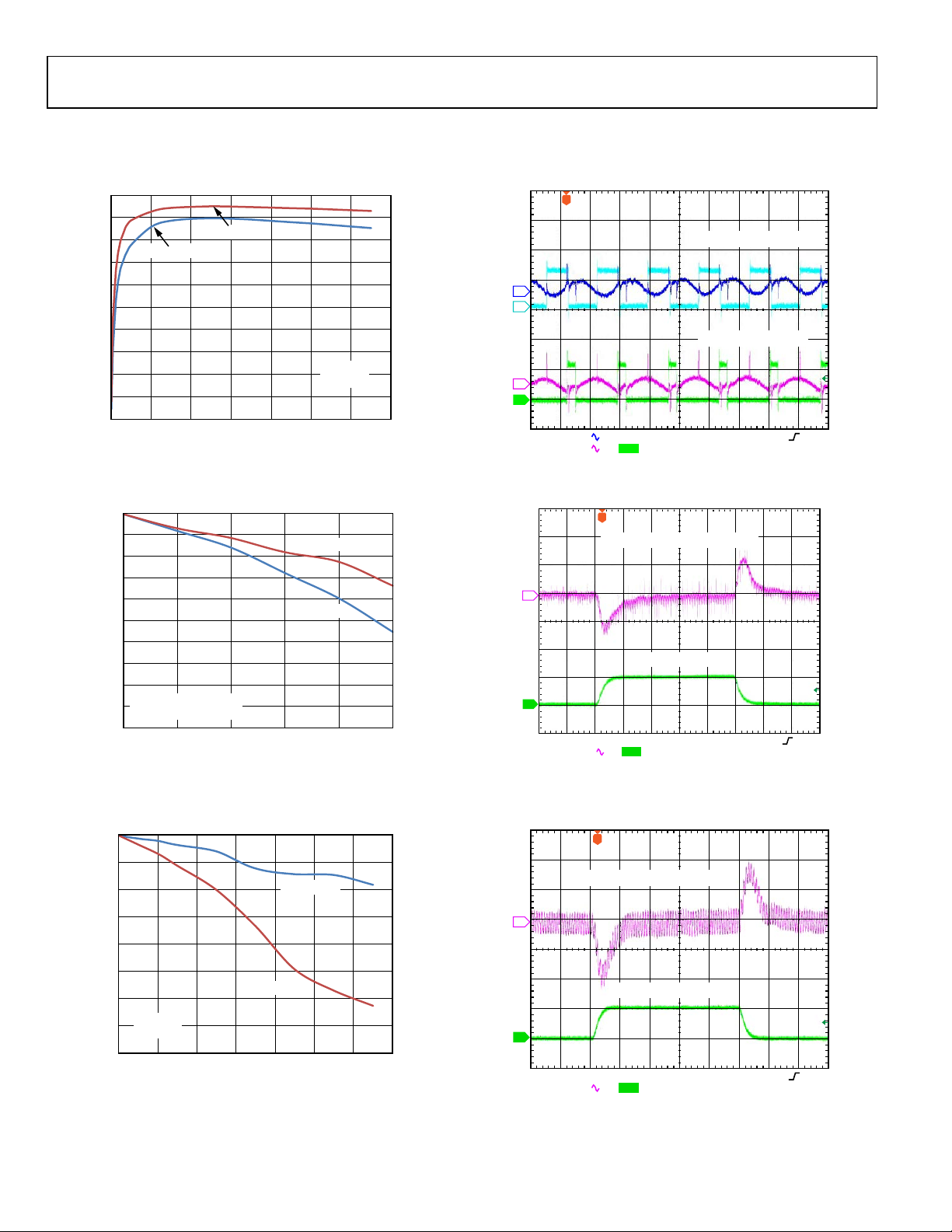
Figure 2. Efficiency (Measurement Is Ma de with the Adjacent Channel Disabled)
Figure 5. Output Ripple, 10 A Load
Figure 3. Line Regulation
Figure 4. Load Regulation
Figure 6. Step Load Transient, V
OUT2
Figure 7. Step Load Transient, V
OUT1
Rev. 0 | Page 4 of 16

Evaluation Board User Guide UG-334
0.035
0.030
0.025
0.020
0.015
0.010
0.005
0
3.0 3.5
4.0 4.5 5.0 5.5 6.0
VINLDO (V)
LINE REGULATION (%)
10272-008
T
A
= 25°C
V
IN
= 12V
–0.02
–0.04
–0.06
–0.08
–0.10
–0.12
–0.14
–0.16
–0.18
–0.20
0
0 0.025 0.050 0.075 0.100 0.125 0.150 0.175 0.200
VOUTLDO LOAD (A)
LOAD REGUL ATION (%)
10272-009
VINLDO = 5V
VINLDO = 3V
T
A
= 25°C
V
IN
= 12V
10272-010
CH1 100mA Ω CH2 50.0mV
M10.0µs A CH1 118mA
1
2
B
W
T
STEP LOAD
1mA TO 200mA
C
INLDO
= 1µF, C
OUTLDO
= 4.7µF
OUTPUT TRANSIENT
Figure 8. VOUTLDO Line Regulation
Figure 10. VOUTLDO Step Load Response
Figure 9. VOUTLDO Load Regulation
Rev. 0 | Page 5 of 16
 Loading...