Filterless, High Efficiency,
Mono 2.5 W Class-D Audio Amplifier
FEATURES
Filterless, Class-D amplifier with spread-spectrum
Σ-Δ modulation
2.5 W into 4 Ω load and 1.4 W into 8 Ω load at 5.0 V supply
with <1% total harmonic distortion plus noise (THD + N)
92% efficiency at 5.0 V, 1.4 W into 8 Ω speaker
>100 dB signal-to-noise ratio (SNR)
High PSRR at 217 Hz: 80 dB
Ultralow EMI emissions
Single-supply operation from 2.5 V to 5.5 V
Gain select function: 6 dB or 12 dB
Fixed input impedance of 80 kΩ
100 nA shutdown current
Short-circuit and thermal protection with autorecovery
Available in a 9-ball, 1.2 mm × 1.2 mm WLCSP
Pop-and-click suppression
APPLICATIONS
Mobile phones
MP3 players
Portable electronics
GENERAL DESCRIPTION
The SSM2377 is a fully integrated, high efficiency, Class-D audio
amplifier. It is designed to maximize performance for mobile
phone applications. The application circuit requires a minimum
of external components and operates from a single 2.5 V to 5.5 V
supply. It is capable of delivering 2.5 W of continuous output power
with <1% THD + N driving a 4 Ω load from a 5.0 V supply.
The SSM2377 features a high efficiency, low noise modulation
scheme that requires no external LC output filters. The modulation operates with high efficiency even at low output power.
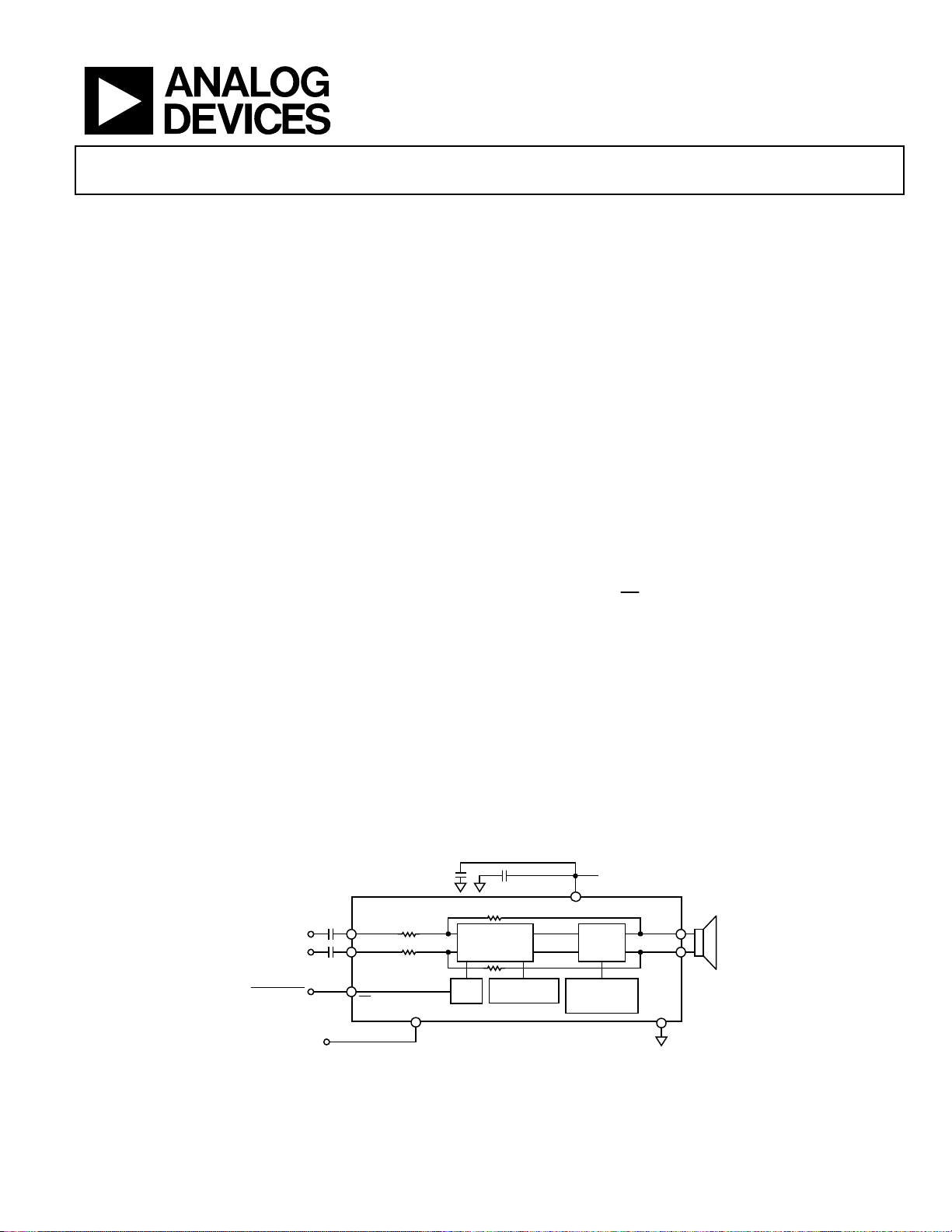
FUNCTIONAL BLOCK DIAGRAM
SSM2377
The SSM2377 operates with 92% efficiency at 1.4 W into 8 Ω
from a 5.0 V supply and has an SNR of >100 dB.
Spread-spectrum pulse density modulation (PDM) is used to
provide lower EMI-radiated emissions compared with other
Class-D architectures. The inherent randomized nature of
spread-spectrum PDM eliminates the clock intermodulation
(beating effect) of several amplifiers in close proximity.
The SSM2377 produces ultralow EMI emissions that significantly reduce the radiated emissions at the Class-D outputs,
particularly above 100 MHz. The SSM2377 passes FCC Class B
radiated emission testing with 50 cm, unshielded speaker cable
without any external filtering. The ultralow EMI emissions of the
SSM2377 are also helpful for antenna and RF sensitivity problems.
The device is configured for either a 6 dB or a 12 dB gain setting
by connecting the GAIN pin to the VDD pin or the GND pin,
respectively. Input impedance is a fixed value of 80 kΩ, independent of the gain select operation.
The SSM2377 has a micropower shutdown mode with a typical
shutdown current of 100 nA. Shutdown is enabled by applying
a logic low to the
The device also includes pop-and-click suppression circuitry,
which minimizes voltage glitches at the output during turn-on
and turn-off, reducing audible noise on activation and deactivation.
Built-in input low-pass filtering is also included to suppress outof-band noise interference to the PDM modulator.
The SSM2377 is specified over the industrial temperature range
of −40°C to +85°C. It has built-in thermal shutdown and output
short-circuit protection. It is available in a halide-free, 9-ball, 0.4 mm
pitch, 1.2 mm × 1.2 mm wafer level chip scale package (WLCSP).
SD
pin.
10µF
SSM2377
AUDIO IN–
AUDIO IN+
SHUTDOWN
GAIN SELECT
Rev. 0
Information furnished by Analog Devices is believed to be accurate and reliable. However, no
responsibility is assumed by Analog Devices for its use, nor for any infringements of patents or other
rights of third parties that may result from its use. Specifications subject to change without notice. No
license is granted by implication or otherwise under any patent or patent rights of Analog Devices.
Trademarks and registered trademarks are the property of their respective owners.
22nF
22nF
GAIN = 6dB O R 12dB
IN+
IN–
SD
80kΩ
80kΩ
BIAS
GAIN
0.1µF
MODULATO R
(Σ-Δ)
INTERNAL
OSCILLATOR
Figure 1.
POWER SUPPLY
2.5V TO 5. 5V
VDD
FET
DRIVER
POP/CLICK
AND EMI
SUPPRESSION
One Technology Way, P.O. Box 9106, Norwood, MA 02062-9106, U.S.A.
Tel: 781.329.4700 www.analog.com
Fax: 781.461.3113 ©2011 Analog Devices, Inc. All rights reserved.
OUT+
OUT–
GND
09824-001

SSM2377
TABLE OF CONTENTS
Features .............................................................................................. 1
Applications ....................................................................................... 1
General Description ......................................................................... 1
Functional Block Diagram .............................................................. 1
Revision History ............................................................................... 2
Specifications ..................................................................................... 3
Absolute Maximum Ratings ............................................................ 5
Thermal Resistance ...................................................................... 5
ESD Caution .................................................................................. 5
Pin Configuration and Function Descriptions ............................. 6
Typical Performance Characteristics ............................................. 7
Typical Application Circuits .......................................................... 12
REVISION HISTORY
5/11—Revision 0: Initial Version
Theory of Operation ...................................................................... 13
Overview ..................................................................................... 13
Gain Selection ............................................................................. 13
Pop-and-Click Suppression ...................................................... 13
EMI Noise .................................................................................... 13
Output Modulation Description .............................................. 13
Layout .......................................................................................... 14
Input Capacitor Selection .......................................................... 14
Power Supply Decoupling ......................................................... 14
Outline Dimensions ....................................................................... 15
Ordering Guide .......................................................................... 15
Rev. 0 | Page 2 of 16

SSM2377
SPECIFICATIONS
VDD = 5.0 V, TA = 25°C, RL = 8 Ω +33 μH, unless otherwise noted.
Table 1.
Parameter Symbol Test Conditions/Comments Min Typ Max Unit
DEVICE CHARACTERISTICS
Output Power P
R
R
R
R
R
R
R
R
R
R
R
R
Efficiency η P
Total Harmonic Distortion
Plus Noise
P
Input Common-Mode Voltage
Range
Common-Mode Rejection
Ratio
Average Switching Frequency fSW 256 kHz
Clock Frequency f
Differential Output Offset
Voltage
POWER SUPPLY
Supply Voltage Range VDD Guaranteed from PSRR test 2.5 5.5 V
Power Supply Rejection Ratio
PSRR
PSRR V
Supply Current ISY V
V
V
V
V
V
Shutdown Current ISD
GAIN CONTROL
Closed-Loop Gain Gain GAIN = GND 12 dB
GAIN = VDD 6 dB
Input Impedance ZIN
SHUTDOWN CONTROL
Input Voltage High VIH 1.35 V
Input Voltage Low VIL 0.35 V
Turn-On Time tWU
Turn-Off Time tSD
Output Impedance Z
f = 1 kHz, 20 kHz BW
OUT
= 8 Ω, THD = 1%, VDD = 5.0 V 1.41 W
L
= 8 Ω, THD = 1%, VDD = 3.6 V 0.72 W
L
= 8 Ω, THD = 1%, VDD = 2.5 V 0.33 W
L
= 8 Ω, THD = 10%, VDD = 5.0 V 1.78 W
L
= 8 Ω, THD = 10%, VDD = 3.6 V 0.90 W
L
= 8 Ω, THD = 10%, VDD = 2.5 V 0.41 W
L
= 4 Ω, THD = 1%, VDD = 5.0 V 2.49 W
L
= 4 Ω, THD = 1%, VDD = 3.6 V 1.25 W
L
= 4 Ω, THD = 1%, VDD = 2.5 V 0.54 W
L
= 4 Ω, THD = 10%, VDD = 5.0 V 3.17
L
= 4 Ω, THD = 10%, VDD = 3.6 V 1.56 W
L
= 4 Ω, THD = 10%, VDD = 2.5 V 0.68 W
L
= 1.4 W into 8 Ω, VDD = 5.0 V 92.4 %
OUT
THD + N P
1.0 VDD − 1 V
V
CM
= 1 W into 8 Ω, f = 1 kHz, VDD = 5.0 V 0.007 %
OUT
= 0.5 W into 8 Ω, f = 1 kHz, VDD = 3.6 V 0.009 %
OUT
1
W
CMRR 100 mV rms at 1 kHz 51 dB
6.2 MHz
OSC
Gain = 6 dB 0.4 5.0 mV
V
OOS
Inputs are ac-grounded, C
= 0.1 μF,
IN
gain = 6 dB
OUT
V
GSM
= 100 mV at 217 Hz 80 dB
RIPPLE
= 100 mV at 1 kHz 80 dB
RIPPLE
= 0 V, no load, VDD = 5.0 V 2.5 mA
IN
= 0 V, no load, VDD = 3.6 V 2.0 mA
IN
= 0 V, no load, VDD = 2.5 V 1.9 mA
IN
= 0 V, RL = 8 Ω + 33 μH, VDD = 5.0 V 2.5 mA
IN
= 0 V, RL = 8 Ω + 33 μH, VDD = 3.6 V 2.0 mA
IN
= 0 V, RL = 8 Ω + 33 μH, VDD = 2.5 V 1.8 mA
IN
= GND
SD
= VDD, gain = 6 dB or 12 dB
SD
rising edge from GND to VDD
SD
falling edge from VDD to GND
SD
= GND
SD
Rev. 0 | Page 3 of 16
100 nA
80 kΩ
12.5 ms
5 μs
100 kΩ

SSM2377
Parameter Symbol Test Conditions/Comments Min Typ Max Unit
NOISE PERFORMANCE
Output Voltage Noise en
f = 20 Hz to 20 kHz, inputs are ac-grounded,
gain = 6 dB, A-weighted
V
V
Signal-to-Noise Ratio SNR P
1
Although the SSM2377 has good audio quality above 3 W, continuous output power beyond 3 W must be avoided due to device packaging limitations.
= 5.0 V 30 μV
DD
= 3.6 V 30 μV
DD
= 1.4 W, RL = 8 Ω, A-weighted 101 dB
OUT
Rev. 0 | Page 4 of 16

SSM2377
ABSOLUTE MAXIMUM RATINGS
Absolute maximum ratings apply at 25°C, unless otherwise noted.
Table 2.
Parameter Rating
Supply Voltage 6 V
Input Voltage V
Common-Mode Input Voltage V
Storage Temperature Range −65°C to +150°C
Operating Temperature Range −40°C to +85°C
Junction Temperature Range −65°C to +165°C
Lead Temperature (Soldering, 60 sec) 300°C
ESD Susceptibility 4 kV
DD
DD
Stresses above those listed under Absolute Maximum Ratings
may cause permanent damage to the device. This is a stress
rating only; functional operation of the device at these or any
other conditions above those indicated in the operational
section of this specification is not implied. Exposure to absolute
maximum rating conditions for extended periods may affect
device reliability.
THERMAL RESISTANCE
Junction-to-air thermal resistance (θJA) is specified for the worstcase conditions, that is, a device soldered in a printed circuit
board (PCB) for surface-mount packages. θ
is determined
JA
according to JEDEC JESD51-9 on a 4-layer PCB with natural
convection cooling.
Table 3. Thermal Resistance
Package Type PCB θJA Unit
9-Ball, 1.2 mm × 1.2 mm WLCSP 2S2P 88 °C/W
ESD CAUTION
Rev. 0 | Page 5 of 16
 Loading...