

Page 1
Audio, Dual-Matched
FEATURES
Very low voltage noise: 1 nV/√Hz maximum @ 100 Hz
Excellent current gain match: 0.5%
Low offset voltage (V
Outstanding offset voltage drift: 0.03 μV/°C
High gain bandwidth product: 200 MHz
GENERAL DESCRIPTION
The SSM2212 is a dual, NPN-matched transistor pair that is
specifically designed to meet the requirements of ultralow noise
audio systems.
With its extremely low input base spreading resistance (rbb' is
typically 28 Ω) and high current gain (h
at I
= 1 mA), the SSM2212 can achieve outstanding signal-to-
C
noise ratios. The high current gain results in superior
performance compared to systems incorporating commercially
available monolithic amplifiers.
Excellent matching of the current gain (Δh
low V
of less than 10 μV typical make the SSM2212 ideal for
OS
symmetrically balanced designs, which reduce high-order
amplifier harmonic distortion.
): 200 μV maximum
OS
typically exceeds 600
FE
) to about 0.5% and
FE
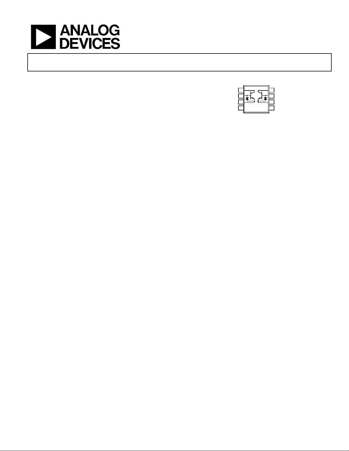
NPN Transistor
SSM2212
PIN CONFIGURATION
1
C
1
2
B
1
3
E
1
NIC
4
SSM2212
NIC = NO INTERNAL CONNECTION
Figure 1. 8-Lead SOIC_N
Stability of the matching parameters is guaranteed by protection
diodes across the base-emitter junction. These diodes prevent
degradation of beta and matching characteristics due to reverse
biasing of the base-emitter junction.
The SSM2212 is also an ideal choice for accurate and reliable
current biasing and mirroring circuits. Furthermore, because a
current mirror’s accuracy degrades exponentially with mismatches
of V
between transistor pairs, the low VOS of the SSM2212
BE
does not need offset trimming in most circuit applications.
The SSM2212 performance and characteristics are guaranteed
over the extended temperature range of −40°C to +85°C.
8
C
2
7
B
2
6
E
2
NIC
5
09043-001
B
Rev.
Information furnished by Analog Devices is believed to be accurate and reliable. However, no
responsibility is assumed by Anal og Devices for its use, nor for any infringements of patents or ot her
rights of third parties that may result from its use. Specifications subject to change without notice. No
license is granted by implication or otherwise under any patent or patent rights of Analog Devices.
Trademarks and registered trademarks are the property of their respective owners.
One Technology Way, P.O. Box 9106, Norwood, MA 02062-9106, U.S.A.
Tel: 781.329.4700 www.analog.com
Fax: 781.461.3113 ©2010 Analog Devices, Inc. All rights reserved.
Page 2

SSM2212
TABLE OF CONTENTS
Features.............................................................................................. 1
Pin Configuration............................................................................. 1
General Description ......................................................................... 1
Revision History ............................................................................... 2
Specifications..................................................................................... 3
Electrical Characteristics ............................................................. 3
Absolute Maximum Ratings............................................................ 4
REVISION HISTORY
7/10—Rev. A to Rev. B
Changes to Figure 1.......................................................................... 1
6/10—Rev. 0 to Rev. A
Changes to Fast Logarithmic Amplifier Section .......................... 8
6/10—Revision 0: Initial Version
Thermal Resistance.......................................................................4
ESD Caution...................................................................................4
Typical Performance Characteristics..............................................5
Applications Information.................................................................8
Fast Logarithmic Amplifier..........................................................8
Outline Dimensions..........................................................................9
Ordering Guide .............................................................................9
Rev. B | Page 2 of 12
Page 3
SSM2212
SPECIFICATIONS
ELECTRICAL CHARACTERISTICS
VCB = 15 V, IO = 10 μA, TA = 25°C, unless otherwise specified.
Table 1.
Parameter Symbol Text Conditions/Comments Min Typ Max Unit
DC AND AC CHARACTERISTICS
Current Gain1 h
I
−40°C ≤ TA ≤ +85°C 300
I
−40°C ≤ TA ≤ +85°C 200
Current Gain Match2 ΔhFE 10 μA ≤ IC ≤ 1 mA 0.5 5 %
Noise Voltage Density3 e
f
f
f
f
Low Frequency Noise (0.1 Hz to 10 Hz) eN p-p IC = 1 mA 0.4 μV p-p
Offset Voltage VOS V
−40°C ≤ TA ≤ +85°C 220 μV
Offset Voltage Change vs. VCB ΔVOS/ΔVCB 0 V ≤ VCB ≤ V
Offset Voltage Change vs. IC ΔVOS/ΔIC 1 μA ≤ IC ≤ 1 mA5, VCB = 0 V 5 70 μV
Offset Voltage Drift ΔVOS/ΔT −40°C ≤ TA ≤ +85°C 0.08 1 μV/°C
−40°C ≤ TA ≤ +85°C, V
Breakdown Voltage BV
Gain Bandwidth Product fT I
Collector-to-Base Leakage Current I
−40°C ≤ TA ≤ +85°C 3 nA
Collector-to-Collector Leakage Current ICC V
−40°C ≤ TA ≤ +85°C 4 nA
Collector-to-Emitter Leakage Current I
−40°C ≤ TA ≤ +85°C 4 nA
Input Bias Current IB I
−40°C ≤ TA ≤ +85°C 50 nA
Input Offset Current IOS I
−40°C ≤ TA ≤ +85°C 13 nA
Input Offset Current Drift ΔIOS/ΔT IC = 10 μA6, −40°C ≤ TA ≤ +85°C 40 150 pA/°C
Collector Saturation Voltage V
Output Capacitance COB V
Bulk Resistance RBE 10 μA ≤ IC ≤ 10 mA6 0.3 1.6 Ω
Collector-to-Collector Capacitance CCC V
1
Current gain is guaranteed with collector-to-base voltage (VCB) swept from 0 V to V
2
Current gain match (ΔhFE) is defined as follows: ΔhFE = (100(ΔIB)(h
3
Noise voltage density is guaranteed, but not 100% tested.
4
This is the maximum change in VOS as VCB is swept from 0 V to 40 V.
5
Measured at IC = 10 μA and guaranteed by design over the specified range of IC.
6
Guaranteed by design.
7
ICC and I
are verified by measurement of I
CES
CBO
.
FE
= 1 mA 300 605
C
= 10 μA 200 550
C
I
N
40 V
CEO
V
CBO
V
CES
I
CE (SAT)
FE min
= 1 mA, VCB = 0 V
C
= 10 Hz 1.6 2 nV/√Hz
O
= 100 Hz 0.9 1 nV/√Hz
O
= 1 kHz 0.85 1 nV/√Hz
O
= 10 kHz 0.85 1 nV/√Hz
O
= 0 V, IC = 1 mA 10 200 μV
CB
4
,1 μA ≤ IC ≤ 1 mA5 10 50 μV
MAX
trimmed to 0 V 0.03 0.3 μV/°C
OS
= 100 mA, VCE = 10 V 200 MHz
C
= V
CB
CC
CE
= 10 μA 50 nA
C
= 10 μA 6.2 nA
C
= 1 mA, IB = 100 μA 0.05 0.2 V
C
CB
CC
)/IC).
25 500 pA
MAX
6, 7
= V
= V
MAX
, VBE = 0 V
MAX
6, 7
35 500 pA
35 500 pA
= 15 V, IE = 0 μA 23 pF
= 0 V 35 pF
at the indicated collector currents.
MAX
Rev. B | Page 3 of 12
Page 4
SSM2212
ABSOLUTE MAXIMUM RATINGS
Table 2.
Parameter Rating
Breakdown Voltage of
Collector-to-Base Voltage (BV
Breakdown Voltage of
Collector-to-Emitter Voltage (BV
Breakdown Voltage of
Collector-to-Collector Voltage (BV
Breakdown Voltage of
Emitter-to-Emitter Voltage (BV
Collector Current (IC) 20 mA
Emitter Current (IE) 20 mA
Storage Temperature Range −65°C to +150°C
Operating Temperature Range −40°C to +85°C
Junction Temperature Range −65°C to +150°C
Lead Temperature (Soldering, 60 sec) 300°C
CBO
)
)
CEO
CC
)
EE
40 V
40 V
40 V
)
40 V
Stresses above those listed under Absolute Maximum Ratings
may cause permanent damage to the device. This is a stress
rating only; functional operation of the device at these or any
other conditions above those indicated in the operational
section of this specification is not implied. Exposure to absolute
maximum rating conditions for extended periods may affect
device reliability.
THERMAL RESISTANCE
θJA is specified for the worst-case conditions, that is, a device
soldered in a circuit board for surface-mount packages.
Table 3. Thermal Resistance
Package Type θJA θ
8-Lead SOIC (R-8) 120 45 °C/W
Unit
JC
ESD CAUTION
Rev. B | Page 4 of 12
Page 5

SSM2212
TYPICAL PERFORMANCE CHARACTERISTICS
TA = 25°C, VCE = 5 V, unless otherwise specified.
CH1 4.92V p-p
1
900
800
700
)
FE
600
500
= +125°C
T
A
TA = +25°C
CH1 2.00V M4.00s A CH1 15.8V
Figure 2. Low Frequency Noise (0.1 Hz to 10 Hz), I
1k
100
= 1µA TEST
I
C
10
1
NOISE VOLTAGE DENSITY (nV/ Hz)
0.1
0.1 1 10 100 1k 10k 100k
= 10µA TEST
I
C
IC = 1mA TEST
FREQUENCY (Hz)
Figure 3. Noise Voltage Density vs. Frequency
100
9043-002
= 1 mA, Gain = 10,000,000
C
400
CURRENT GAIN (h
300
200
100
0.001 10.10.01
COLLECT OR CURRENT (mA)
Figure 5. Current Gain vs. Collector Current (V
= –55°C
T
A
= 0 V)
CB
09043-005
900
800
700
)
FE
600
500
400
300
CURRENT GAIN (h
200
100
0
–100 –50 0 50 100 150
09043-003
TEMPERATURE ( °C)
Figure 6. Current Gain vs. Temperature (Excludes I
1mA
1µA
CBO
09043-006
)
0.70
80
60
40
TOTAL NOISE (nV/ Hz)
20
0
0.001 10.10.01
RS = 100kΩ
R
= 10kΩ
S
R
= 1kΩ
S
COLLECT OR CURRENT, IC (mA)
Figure 4. Total Noise vs. Collector Current, f = 1 kHz
09043-004
Rev. B | Page 5 of 12
0.65
(V)
0.60
BE
0.55
0.50
0.45
0.40
BASE EMITTER VOLTAGE, V
0.35
0.30
0.001 0.01 0.1 1 10
COLLECT O R CURRENT, IC (mA)
VCE = 5V
Figure 7. Base Emitter Voltage vs. Collector Current
09043-008
Page 6

SSM2212
h
100
1000
10
(MΩ)
IE
1
VCE = 5V
0.1
INPUT RESI STANCE,
0.01
0.001
0.001 0.01 0.1 1 10
COLLECT O R CURRENT, IC (mA)
Figure 8. Small Signal Input Resistance vs. Collector Current
1m
0.1m
(mho)
OE
0.01m
VCE = 5V
1µ
CONDUCTANCE, h
0.1µ
100
(nA)
10
CBO
1
CURRENT, I
0.1
0.01
25 50 75 100 125
09043-009
TEMPERATURE ( °C)
09043-012
Figure 11. Collector-to-Base Leakage Current vs. Temperature
40
35
30
(pF)
25
CB
20
15
CAPACITANCE, C
10
5
0.01µ
0.001 10001001010.10.01
COLLECT OR CURRENT, IC (mA)
Figure 9. Small Signal Output Conductance vs. Collector Current
100
(mA)
C
COLLECT OR CURRENT, I
TA = –55°C
10
T
A
1
0.1
0.01
0 0.1 0.2 0.3 0.4 0.5 0. 6 0.7 0.8 0.9
SATURATION V OLTAGE, V
= +25°C
T
= +125°C
A
SAT
(V)
Figure 10. Collector Current vs. Saturation Voltage
0
0 102030405
09043-010
REVERSE BIAS VO LTAGE (V)
0
09043-013
Figure 12. Collector-to-Base Capacitance vs. Reverse Bias Voltage
40
35
30
(pF)
25
CC
20
15
CAPACITANCE, C
10
5
0
09043-017
0 102030405
COLLECTOR-TO-SUBSTRATE VOL T AGE (V)
0
09043-014
Figure 13. Collector-to-Collector Capacitance vs.
Collector-to-Substrate Voltage
Rev. B | Page 6 of 12
Page 7

SSM2212
1000
100
(nA)
10
CC
1
CURRENT, I
0.1
4.0
3.5
3.0
(pF)
2.5
CC
2.0
1.5
CAPACITANCE, C
1.0
0.5
0.01
25 50 75 100 125
TEMPERATURE ( °C)
Figure 14. Collector-to-Collector Leakage Current vs. Temperature
0
0 102030405
09043-015
REVERSE BIAS VO LTAGE (V)
0
09043-016
Figure 15. Collector-to-Collector Capacitance vs. Reverse Bias Voltage
Rev. B | Page 7 of 12
Page 8

SSM2212
V
V
APPLICATIONS INFORMATION
FAST LOGARITHMIC AMPLIFIER
The circuit of Figure 16 is a modification of a standard
logarithmic amplifier configuration. Running the SSM2212 at
2.5 mA per side (full-scale) allows for a fast response with a wide
dynamic range. The circuit has a 7 decade current range and a
5 decade voltage range, and it is capable of 2.5 μs settling time to
1% with a 1 V to 10 V step. The output follows the equation:
V
kT
RR
V ln
=
O
23 +
R
2
REF
V
q
IN
R
S
4kΩ
V
IN
(0V TO 10V)
To compensate for the temperature dependence of the kT/q term, a
resistor with a positive 0.35%/°C temperature coefficient is chosen
for R
. The output is inverted with respect to the input and is
2
nominally −1 V/decade using the component values indicated.
+15
2
8
3
330pF
AD8512
–15V
1
4
R
3
7.5kΩ
V
O
4kΩ
SSM2212
R
2
500Ω
= TEL L ABS QB1E (+0. 35% /°C)
R
2
09043-018
REF
10V
R
4kΩ
330pF
1
6
7
1/2
AD8512
5
Figure 16. Fast Logarithmic Amplifier
Rev. B | Page 8 of 12
Page 9

SSM2212
OUTLINE DIMENSIONS
5.00(0.1968)
4.80(0.1890)
4.00 (0.1574)
3.80 (0.1497)
0.25 (0.0098)
0.10 (0.0040)
COPLANARITY
0.10
CONTROLLING DIMENSIONS ARE IN MILLIMETERS; INCH DIMENSIONS
(IN PARENTHESES) ARE ROUNDED-OFF MILLIMETER EQUIVALENTSFOR
REFERENCE ONLYAND ARE NOT APPROPRIATE FOR USE IN DESIGN.
85
1
1.27 (0.0500)
SEATING
PLANE
COMPLIANT TO JEDEC STANDARDS MS-012-AA
BSC
6.20 (0.2441)
5.80 (0.2284)
4
1.75 (0.0688)
1.35 (0.0532)
0.51 (0.0201)
0.31 (0.0122)
8°
0°
0.25 (0.0098)
0.17 (0.0067)
0.50 (0.0196)
0.25 (0.0099)
1.27 (0.0500)
0.40 (0.0157)
45°
012407-A
Figure 17. 8-Lead Standard Small Outline Package [SOIC_N]
Narrow Body
(R-8)
Dimensions shown in millimeters and (inches)
ORDERING GUIDE
Model1 Temperature Range Package Description Package Option
SSM2212RZ −40°C to +85°C 8-Lead Standard Small Outline Package [SOIC_N] R-8
SSM2212RZ-R7 −40°C to +85°C 8-Lead Standard Small Outline Package [SOIC_N] R-8
SSM2212RZ-RL −40°C to +85°C 8-Lead Standard Small Outline Package [SOIC_N] R-8
1
Z = RoHS Compliant Part.
Rev. B | Page 9 of 12
Page 10

SSM2212
NOTES
Rev. B | Page 10 of 12
Page 11

SSM2212
NOTES
Rev. B | Page 11 of 12
Page 12

SSM2212
NOTES
©2010 Analog Devices, Inc. All rights reserved. Trademarks and
registered trademarks are the property of their respective owners.
D09043-0-7/10(B)
Rev. B | Page 12 of 12
 Loading...