

Low Distortion 1.5 Watt
FEATURES
1.5 W output
Differential (BTL2) output
Single-supply operation: 2.7 V to 5.5 V
Functions down to 1.75 V
Wide bandwidth: 4 MHz
Highly stable, phase margin: >80 degrees
Low distortion: 0.2% THD @ 1 W output
Excellent power-supply rejection
APPLICATIONS
Portable computers
Personal wireless communicators
Hands-free telephones
Speaker phones
Intercoms
Musical toys and talking games
GENERAL DESCRIPTION
The SSM22113 is a high performance audio amplifier that
delivers 1 W rms of low distortion audio power into a bridgeconnected 8 Ω speaker load (or 1.5 W rms into 4 Ω load). It
operates over a wide temperature range and is specified for
single-supply voltages between 2.7 V and 5.5 V. When operating from batteries, it continues to operate down to 1.75 V.
This makes the SSM2211 the best choice for unregulated
applications, such as toys and games. Featuring a 4 MHz
bandwidth and distortion below 0.2% THD @ 1 W, superior
performance is delivered at higher power or lower speaker
load impedance than competitive units.
The low differential dc output voltage results in negligible
losses in the speaker winding, and makes high value dc
blocking capacitors unnecessary. Battery life is extended by
using shutdown mode, which typically reduces quiescent
current drain to 100 nA.
1
Audio Power Amplifier
SSM2211
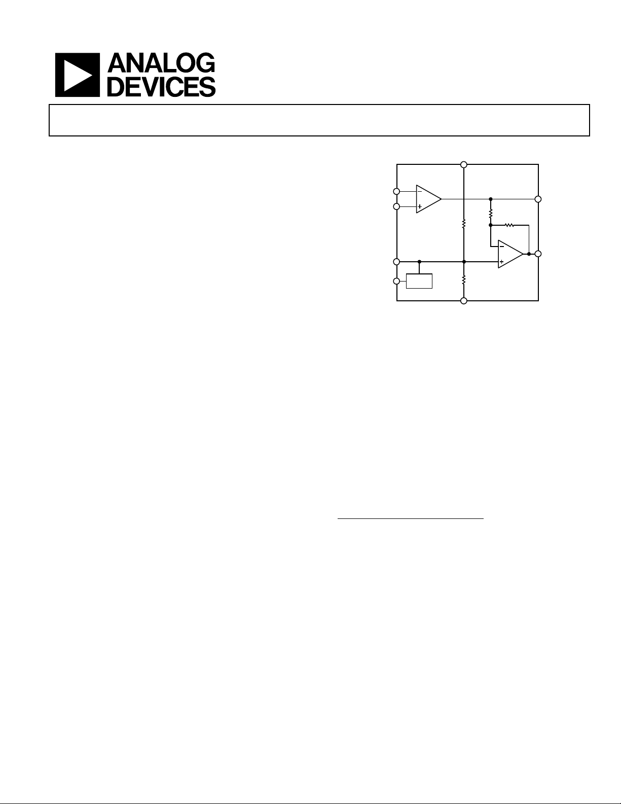
FUNCTIONAL BLOCK DIAGRAM
IN–
IN+
BYPASS
SHUTDOWN
BIAS
SSM2211
V– (GND)
Figure 1.
The SSM2211 is designed to operate over the −20°C to +85°C
temperature range. The SSM2211 is available in SOIC-8 and
LFCSP (lead frame chip scale) surface mount packages. The
advanced mechanical packaging of the SSM2211CP ensures
lower chip temperature and enhanced performance relative to
standard packaging options.
Applications include personal portable computers, hands-free
telephones and transceivers, talking toys, intercom systems, and
other low voltage audio systems requiring 1 W output power.
1
1.5 W @ 4 Ω 25°C ambient, < 1% THD, 5 V supply, 4-layer PCB.
2
Bridge-tied load.
3
Protected by U.S. Patent No. 5,519,576.
V
A
OUT
V
B
OUT
00358-001
Rev. C
Information furnished by Analog Devices is believed to be accurate and reliable.
However, no responsibility is assumed by Analog Devices for its use, nor for any
infringements of patents or other rights of third parties that may result from its use.
Specifications subject to change without notice. No license is granted by implication
or otherwise under any patent or patent rights of Analog Devices. Trademarks and
registered trademarks are the property of their respective owners.
One Technology Way, P.O. Box 9106, Norwood, MA 02062-9106, U.S.A.
Tel: 781.329.4700
Fax: 781.326.8703 © 2004 Analog Devices, Inc. All rights reserved.
www.analog.com

SSM2211
TABLE OF CONTENTS
Electrical Characteristics................................................................. 3
Absolute Maximum Ratings............................................................ 4
Pin Configurations ...........................................................................5
Typical Performance Characteristics............................................. 6
Product Overview........................................................................... 13
Thermal Performance—LFCSP................................................ 13
Typical Application......................................................................... 14
Bridged Output vs. Single-Ended Output Configurations ... 14
Speaker Efficiency and Loudness .............................................14
Power Dissipation....................................................................... 15
Output Voltage Headroom........................................................ 16
REVISION HISTORY
10/04—Data Sheet Changed from Rev. B to Rev. C
Updated Format..................................................................Universal
Changes to General Description .................................................... 1
Changes to Table 5............................................................................ 4
Deleted Thermal Performance—SOIC Section ........................... 8
Changes to Figure 31...................................................................... 10
Changes to Figure 40...................................................................... 12
Changes to Thermal Performance—LFCSP Section .................13
Deleted Figure 52, Renumbered Successive Figures.................. 14
Deleted Printed Circuit Board Layout —SOIC Section............ 14
Changes to Output Voltage Headroom Section .........................16
Changes to Start-Up Popping Noise Section .............................. 17
Changes to Ordering Guide.......................................................... 20
Automatic Shutdown-Sensing Circuit..................................... 16
Shutdown-Circuit Design Example......................................... 17
Start-Up Popping Noise............................................................. 17
SSM2211 Amplifier Design Example.................................. 17
Single-Ended Applications........................................................ 18
Driving Two Speakers Single Endedly..................................... 18
Evaluation Board ........................................................................ 19
LFCSP Printed Circuit Board Layout Considerations .......... 19
Outline Dimensions .......................................................................20
Ordering Guide .......................................................................... 20
10/02–Data Sheet Changed from Rev. A to Rev. B
Deleted 8-Lead PDIP .........................................................Universal
Updated OUTLINE DIMENSIONS ............................................ 15
5/02–Data Sheet Changed from Rev. 0 to Rev. A
Edits to GENERAL DESCRIPTION...............................................1
Edits to PACKAGE TYPE ................................................................3
Edits to ORDERING GUIDE ..........................................................3
Edits to PRODUCT OVERVIEW ...................................................8
Edits to PRINTED CIRCUIT BOARD LAYOUT
CONSIDERATION........................................................................ 13
Added section PRINTED CIRCUIT BOARD LAYOUT
CONSIDERATION—LFCSP........................................................ 14
Rev. C | Page 2 of 20
SSM2211
ELECTRICAL CHARACTERISTICS
Table 1. V
Parameter Symbol Conditions Min Typ Max Unit
GENERAL CHARACTERISTICS
Differential Output Offset Voltage V
Output Impedance Z
SHUTDOWN CONTROL
Input Voltage High VIH ISY = < 100 mA 3.0 V
Input Voltage Low VIL ISY = normal 1.3 V
POWER SUPPLY
Power-Supply Rejection Ratio PSRR VS = 4.75 V to 5.25 V 66 dB
Supply Current ISY VO1 = VO2 = 2.5 V 9.5 mA
Supply Current, Shutdown Mode ISD Pin 1 = VDD; see Figure 32 100 nA
DYNAMIC PERFORMANCE
Gain Bandwidth GBP 4 MHz
Phase Margin Ø0 86 Degrees
AUDIO PERFORMANCE
Total Harmonic Distortion THD + N
Total Harmonic Distortion THD + N
Voltage Noise Density en f = 1 kHz 85
= 5.0 V, TA = 25°C, RL = 8 Ω, CB = 0.1 µF, VCM = VD/2, unless otherwise noted.
S
AVD = 2 4 50 mV
OOS
0.1
OUT
P = 0.5 W into 8 Ω, f = 1 kHz
P = 1.0 W into 8 Ω, f = 1 kHz
Ω
0.15 %
0.2 %
nV√Hz
Table 2. V
= 3.3 V, TA = 25°C, RL = 8 Ω, CB = 0.1 µF, VCM = VD/2, unless otherwise noted.
S
Parameter Symbol Conditions Min Typ Max Unit
GENERAL CHARACTERISTICS
Differential Output Offset Voltage V
Output Impedance Z
AVD = 2 5 50 mV
OOS
0.1
OUT
Ω
SHUTDOWN INPUT
Input Voltage High VIH ISY = < 100 µA 1.7 V
Input Voltage Low VIL 1 V
POWER SUPPLY
Supply Current ISY VO1 = VO2 = 1.65 V 5.2 mA
Supply Current, Shutdown Mode ISD Pin 1 = VDD; see Figure 32 100 nA
AUDIO PERFORMANCE
Total Harmonic Distortion THD + N
P = 0.35 W into 8 Ω, f = 1 kHz
0.1 %
Table 3. V
= 2.7 V, TA = 25°C, RL = 8 Ω, CB = 0.1 µF, VCM = VS/2, unless otherwise noted.
S
Parameter Symbol Conditions Min Typ Max Unit
GENERAL CHARACTERISTICS
Differential Output Offset Voltage V
Output Impedance Z
AVD = 2 5 50 mV
OOS
0.1
OUT
Ω
SHUTDOWN CONTROL
Input Voltage High VIH ISY = < 100 mA 1.5 V
Input Voltage Low VIL ISY = normal 0.8 V
POWER SUPPLY
Supply Current ISY VO1 = VO2 = 1.35 V 4.2 mA
Supply Current, Shutdown Mode ISD Pin 1 = VDD; see Figure 32 100 nA
AUDIO PERFORMANCE
Total Harmonic Distortion THD + N
P = 0.25 W into 8 Ω, f = 1 kHz
0.1 %
Rev. C | Page 3 of 20
SSM2211
ABSOLUTE MAXIMUM RATINGS
Absolute maximum ratings apply at 25°C, unless otherwise
noted.
Table 4.
Parameter Value
Supply Voltage 6 V
Input Voltage V
Common-Mode Input Voltage V
DD
DD
ESD Susceptibility 2000 V
Storage Temperature Range −65°C to +150°C
Operating Temperature Range −20°C to +85°C
Junction Temperature Range −65°C to +165°C
Lead Temperature Range (Soldering, 60 sec) 300°C
Table 5.
Package Type
8-Lead LFCSP (CP)
8-Lead SOIC (S)
2
θ
JA
1
50 °C/W
121 °C/W
Units
1
For the LFCSP, θJA is measured with exposed lead frame soldered to the
printed circuit board.
2
For the SOIC, θJA is measured with the device soldered to a 4-layer printed
circuit board.
Stresses above those listed under Absolute Maximum Ratings
may cause permanent damage to the device. This is a stress
rating only; the functional operation of the device at these or
any other conditions above those indicated in the operational
sections of this specification is not implied. Exposure to
absolute maximum rating conditions for extended periods may
affect device reliability.
ESD CAUTION
ESD (electrostatic discharge) sensitive device. Electrostatic charges as high as 4000 V readily accumulate on
the human body and test equipment and can discharge without detection. Although this product features
proprietary ESD protection circuitry, permanent damage may occur on devices subjected to high energy
electrostatic discharges. Therefore, proper ESD precautions are recommended to avoid performance
degradation or loss of functionality.
Rev. C | Page 4 of 20
SSM2211
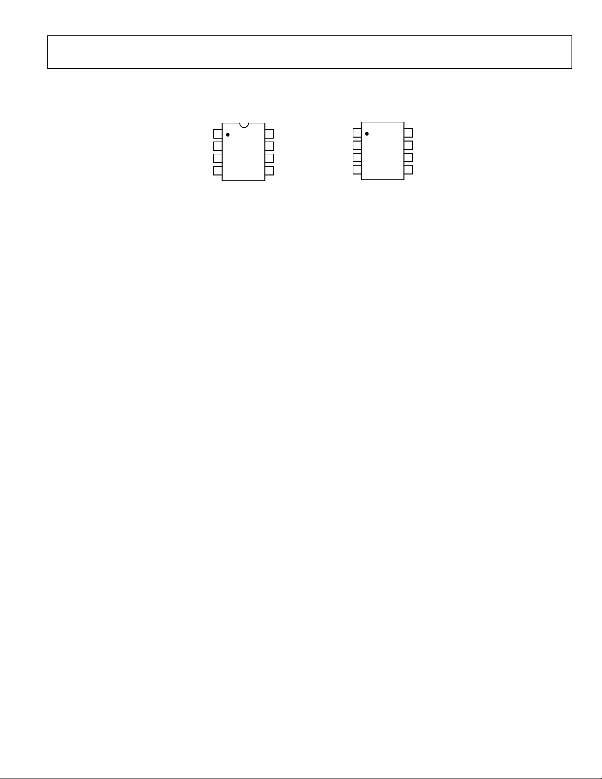
PIN CONFIGURATIONS
SHUTDOWN
BYPASS
IN+
IN–
1
2
TOP VIEW
(Not to Scale)
3
4
Figure 2. 8-Lead SOIC (SO-8)
IN+
IN–
1
2
TOP VIEW
(Not to Scale)
3
4
B
A
00358-002
SHUTDOWN
BYPASS
8
V
OUT
7
V–
V+
6
V
5
OUT
Figure 3. 8-Lead LFCSP (CP-8)
8
V
B
OUT
7
V–
6
V+
5
V
A
OUT
00358-003
Rev. C | Page 5 of 20
SSM2211
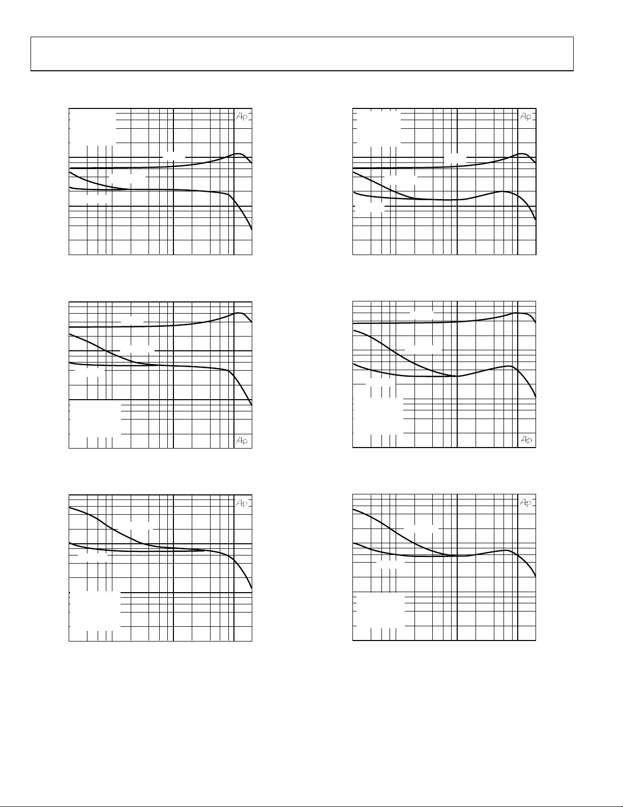
TYPICAL PERFORMANCE CHARACTERISTICS
10
TA = 25°C
= 5V
V
DD
A
= 2 (BTL)
VD
= 8Ω
R
L
P
= 500mW
L
1
CB = 0
10
1
TA = 25°C
= 5V
V
DD
A
= 2 (BTL)
VD
R
= 8Ω
L
= 1W
P
L
CB = 0
CB = 0.1µF
THD + N (%)
CB = 1µF
0.1
0.01
20 100 20k
FREQUENCY (Hz)
1k 10k
Figure 4. THD + N vs. Fre quency
10
CB = 0
1
CB = 1µF
THD + N (%)
0.1
TA = 25°C
V
= 5V
DD
= 10 (BTL)
A
VD
R
= 8Ω
L
P
= 500mW
L
0.01
20 100 20k
CB = 0.1µF
1k 10k
FREQUENCY (Hz)
Figure 5. THD + N vs. Fre quency
10
00358-004
00358-005
CB = 0.1µF
THD + N (%)
0.1
CB = 1µF
0.01
20 100 20k
FREQUENCY (Hz)
1k 10k
Figure 7. THD + N vs. Fre quency
10
CB = 0
1
THD + N (%)
CB = 1µF
0.1
TA = 25°C
= 5V
V
DD
AVD = 10 (BTL)
R
= 8Ω
L
= 1W
P
L
0.01
20 100 20k
CB = 0.1µF
1k 10k
FREQUENCY (Hz)
Figure 8. THD + N vs. Fre quency
10
00358-007
00358-008
CB = 0.1µF
1
CB = 1µF
THD + N (%)
0.1
TA = 25°C
V
= 5V
DD
= 20 (BTL)
A
VD
= 8Ω
R
L
P
= 500mW
L
0.01
20 100 20k
FREQUENCY (Hz)
1k 10k
Figure 6. THD + N vs. Fre quency
00358-006
Rev. C | Page 6 of 20
CB = 0.1µF
1
CB = 1µF
THD + N (%)
0.1
TA = 25°C
= 5V
V
DD
= 20 (BTL)
A
VD
R
= 8Ω
L
= 1W
P
L
0.01
20 100 20k
FREQUENCY (Hz)
1k 10k
Figure 9. THD + N vs. Fre quency
00358-009
 Loading...