Analog Devices SSM2135S, SSM2135P Datasheet

Dual Single-Supply
SSM2135
V+
OUT B
–IN B
+IN B
OUT A
–IN A
+IN A
V–/GND
SSM2135
OUT A
–IN A
+IN A
V–/GND
1
2
3
4
8
7
6
5
V+
OUT B
–IN B
+IN B
a
FEATURES
Excellent Sonic Characteristics
High Output Drive Capability
5.2 nV/√
0.001% THD+N (V
3.5 MHz Gain Bandwidth
Unity-Gain Stable
Low Cost
APPLICATIONS
Multimedia Audio Systems
Microphone Preamplifier
Headphone Driver
Differential Line Receiver
Balanced Line Driver
Audio ADC Input Buffer
Audio DAC l-V Converter and Filter
Pseudo-Ground Generator
GENERAL DESCRIPTION
The SSM2135 Dual Audio Operational Amplifier permits
excellent performance in portable or low power audio systems,
with an operating supply range of +4 V to +36 V or ±2 V to
±18 V. The unity gain stable device has very low voltage noise
of 4.7 nV/√
0.01% over normal signal levels and loads. Such characteristics
are enhanced by wide output swing and load drive capability. A
unique output stage* permits output swing approaching the rail
Hz Equivalent Input Noise @ 1 kHz
= 2.5 V p-p @ 1 kHz)
O
Hz, and total harmonic distortion plus noise below
Audio Operational Amplifier
SSM2135
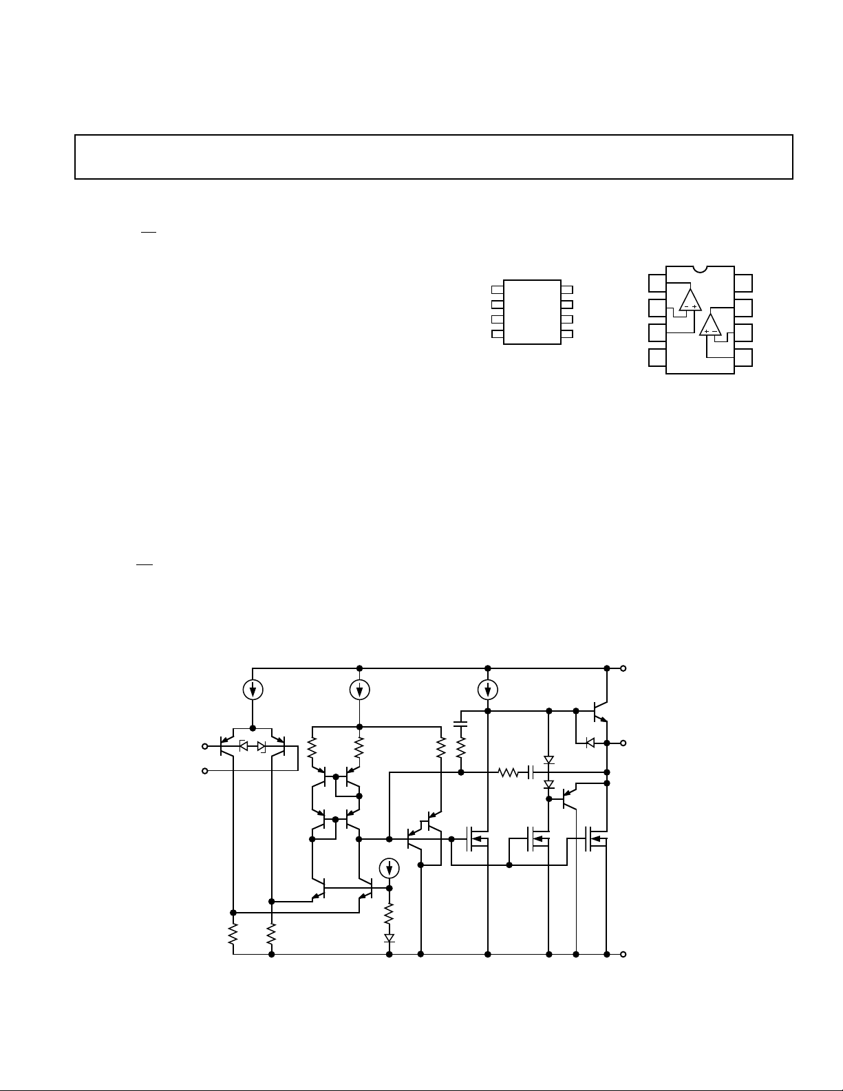
PIN CONNECTIONS
8-Lead Narrow-Body SOIC
(S Suffix) (P-Suffix)
under moderate load conditions. Under severe loading, the
SSM2135 still maintains a wide output swing with ultralow
distortion.
Particularly well suited for computer audio systems and
portable digital audio units, the SSM2135 can perform
preamplification, headphone and speaker driving, and balanced
line driving and receiving. Additionally, the device is ideal for
input signal conditioning in single-supply sigma-delta analogto-digital converter subsystems such as the AD1878/AD1879.
The SSM2135 is available in 8-lead plastic DIP and SOIC
packages, and is guaranteed for operation over the extended
industrial temperature range of –40°C to +85°C.
*Protected by U. S. Patent No. 5,146,181.
8-Lead Epoxy DIP
FUNCTIONAL BLOCK DIAGRAM
+IN
–IN
9V
9V
REV. D
Information furnished by Analog Devices is believed to be accurate and
reliable. However, no responsibility is assumed by Analog Devices for its
use, nor for any infringements of patents or other rights of third parties
which may result from its use. No license is granted by implication or
otherwise under any patent or patent rights of Analog Devices.
V+
OUT
V–/GND
One Technology Way, P.O. Box 9106, Norwood, MA 02062-9106, U.S.A.
Tel: 617/329-4700 Fax: 617/326-8703

(VS = +5 V, –408C < TA < +858C unless otherwise noted.
SSM2135–SPECIFICA TIONS
Typical specifications apply at TA = +258C.)
Parameter Symbol Conditions Min Typ Max Units
AUDIO PERFORMANCE
Voltage Noise Density e
Current Noise Density i
n
n
f = 1 kHz 5.2 nV/√Hz
f = 1 kHz 0.5 pA/√Hz
Signal-To-Noise Ratio SNR 20 Hz to 20 kHz, 0 dBu = 0.775 V rms 121 dBu
Headroom HR Clip Point = 1% THD+N, f = 1 kHz, R
Total Harmonic Distortion THD+N A
= +1, VO = 1 V p-p, f = 1 kHz, 80 kHz LPF
V
R
= 10 kΩ 0.003 %
L
= 10 kΩ 5.3 dBu
L
RL = 32 Ω 0.005 %
DYNAMIC PERFORMANCE
Slew Rate SR R
= 2 kΩ, TA = +25°C 0.6 0.9 V/µs
L
Gain Bandwidth Product GBW 3.5 MHz
Settling Time t
S
to 0.1%, 2 V Step 5.8 µs
INPUT CHARACTERISTICS
Input Voltage Range V
Input Offset Voltage V
Input Bias Current I
Input Offset Current I
Differential Input Impedance Z
B
OS
CM
OS
IN
V
= 2 V 0.2 2.0 mV
OUT
VCM = 0 V, V
VCM = 0 V, V
Common-Mode Rejection CMR 0 V ≤ V
Large Signal Voltage Gain A
VO
0.01 V ≤ V
= 2 V 300 750 nA
OUT
= 2 V 50 nA
OUT
≤ 4 V, f = dc 87 112 dB
CM
≤ 3.9 V, RL = 600 Ω 2V/µV
OUT
0 +4.0 V
4MΩ
OUTPUT CHARACTERISTICS
Output Voltage Swing High V
Output Voltage Swing Low V
Short Circuit Current Limit I
OH
OL
SC
RL = 100 kΩ 4.1 V
R
= 600 Ω 3.9 V
L
RL = 100 kΩ 3.5 mV
R
= 600 Ω 3.0 mV
L
±30 mA
POWER SUPPLY
Supply Voltage Range V
S
Single Supply +4 +36 V
Dual Supply ±2 ±18 V
Power Supply Rejection Ratio PSRR V
Supply Current I
SY
= +4 V to +6 V, f = dc 90 120 dB
S
V
= 2.0 V, No Load
OUT
V
= +5 V 2.8 6.0 mA
S
VS = ±18 V, V
= 0 V, No Load 3.7 7.6 mA
OUT
ABSOLUTE MAXIMUM RATINGS
Supply Voltage
Single Supply . . . . . . . . . . . . . . . . . . . . . . . . . . . . . . . +36 V
Dual Supply . . . . . . . . . . . . . . . . . . . . . . . . . . . . . . . .±18 V
Input Voltage . . . . . . . . . . . . . . . . . . . . . . . . . . . . . . . . . . .±V
Differential Input Voltage . . . . . . . . . . . . . . . . . . . . . . . . 10 V
Output Short Circuit Duration . . . . . . . . . . . . . . . . Indefinite
Storage Temperature Range . . . . . . . . . . . . –65°C to +150°C
Operating Temperature Range . . . . . . . . . . . –40°C to +85°C
Junction Temperature Range (T
) . . . . . . . . –65°C to +150°C
J
Lead Temperature (Soldering, 60 sec) . . . . . . . . . . . .+300°C
ESD RATINGS
883 (Human Body) Model . . . . . . . . . . . . . . . . . . . . . . . 1 kV
EIAJ Model . . . . . . . . . . . . . . . . . . . . . . . . . . . . . . . . . . 175 V
THERMAL CHARACTERISTICS
Thermal Resistance
8-Lead Plastic DIP θ
S
8-Lead SOIC θ
1
θJA is specified for worst case conditions, i.e., θJA is specified for device in
socket for P-DIP and device soldered in circuit board for SOIC package.
1
JA
θ
JC
JA
θ
JC
ORDERING GUIDE
Temperature Package Package
Model Range Description Option
SSM2135P –40°C to +85°C 8-Lead Plastic DIP N-8
SSM2135S –40°C to +85°C 8-Lead SOIC SO-8
–2–
103°C/W
43°C/W
158°C/W
43°C/W
REV. D

+5V
10
0.1
0.001
10 100 10k1k
1
0.01
LOAD RESISTANCE – Ω
THD – %
VS = +5V
A
V
=
+1, ƒ = 1kHz
V
IN
=
1Vp-p
R
L
= 10kΩ
WITH 80kHz FILTER
1
0.001
020 6040
0.01
10
0.1
30 50
VS = +5V
R
L
=
100kΩ
V
OUT
=
2.5Vp-p
ƒ = 1kHz
WITH 80kHz FILTER
GAIN – dB
THD+N – %
NONINVERTING
INVERTING
500µF
+
R
L
+2.5Vdc
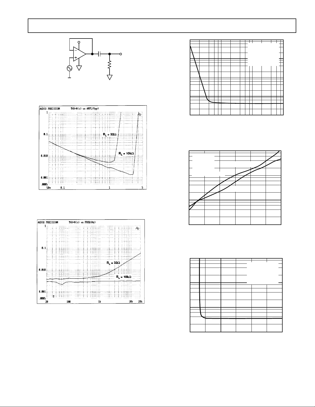
Figure 1. Test Circuit for Figures 2–4
SSM2135
Figure 4. THD+N vs. Load (See Test Circuit)
Figure 2. THD+N vs. Amplitude (See Test Circuit; AV = +1,
V
= +5 V, f = 1 kHz, with 80 kHz Low-Pass Filter)
S
Figure 3. THD+N vs. Frequency (See Test Circuit;
= +1, VIN = 1 V p-p, with 80 kHz Low-Pass Filter)
A
V
Figure 5. THD+N vs. Gain
1
0.1
THD+N – %
0.01
0.001
51525
10 3020
SUPPLY VOLTAGE – V
Figure 6. THD+N vs. Supply Voltage
VS = +5V
+1, ƒ = 1kHz
A
V
=
1Vp-p
V
IN
=
= 10kΩ
R
L
WITH 80kHz FILTER
REV. D
–3–

SSM2135
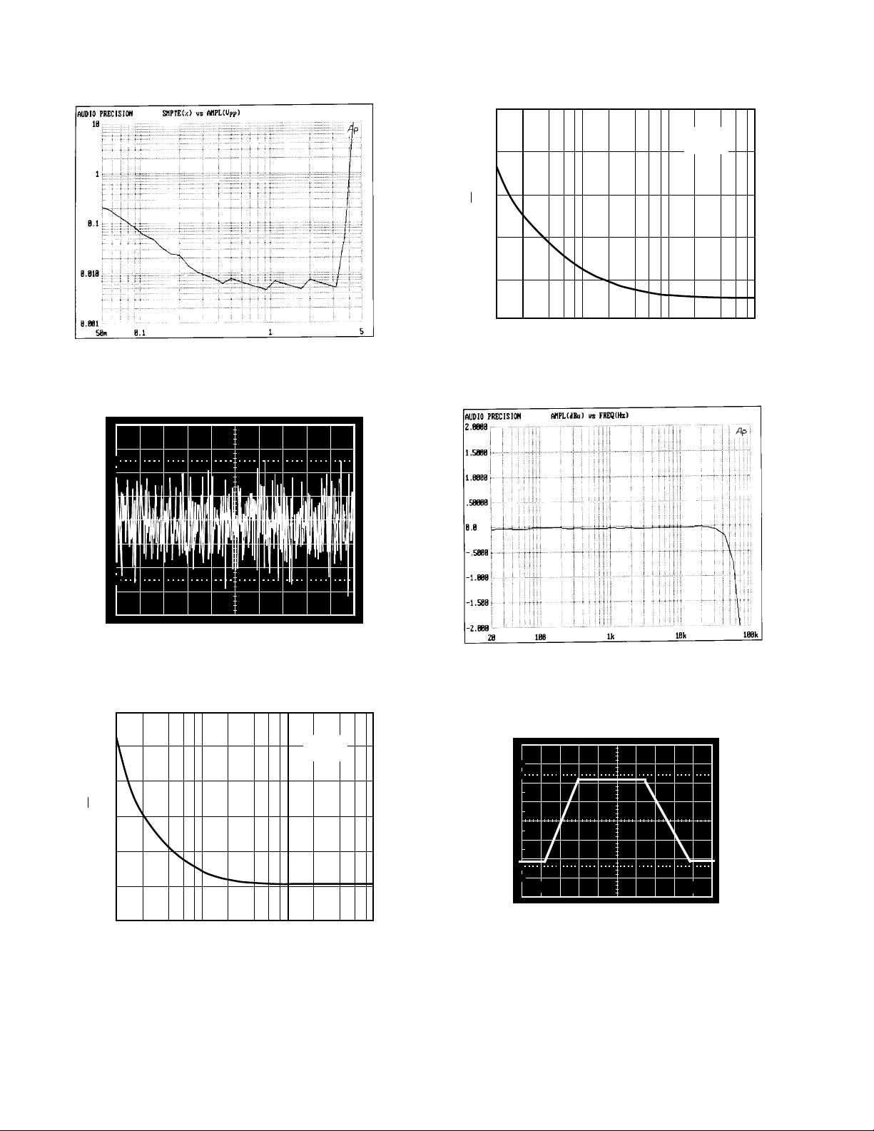
Figure 7. SMPTE Intermodulation Distortion (AV = +1,
= +5 V, f = 1 kHz, RL = 10 kΩ)
V
S
1s
100
90
5
VS = +5V
T
= +25°C
4
3
Hz
√
– pA/
n
i
2
1
0
110 1k100
FREQUENCY – Hz
A
Figure 10. Current Noise Density vs. Frequency
10
0%
Figure 8. Input Voltage Noise (20 nV/div)
30
25
20
Hz
√
15
– nV/
n
e
10
5
0
110 1k100
FREQUENCY – Hz
VS = +5V
TA = +25°C
Figure 9. Voltage Noise Density vs. Frequency
Figure 11. Frequency Response (AV = +1, VS = +5 V,
V
= 1 V p-p, RL = 10 kΩ)
IN
100
90
10
0%
500mV
1µS
Figure 12. Square Wave Response (VS = +5 V, AV = +1,
R
= ∞)
L
–4–
REV. D
 Loading...