Analog Devices OP279, OP179 Datasheet

Rail-to-Rail High Output
OUT A
–IN A
+IN A
–V
+V
OUT B
–IN B
+IN B
OP279
a
FEATURES
Rail-to-Rail Inputs and Outputs
High Output Current: ⴞ60 mA
Single Supply: +5 V to +12 V
Wide Bandwidth: 5 MHz
High Slew Rate: 3 V/s
Low Distortion: 0.01%
Unity-Gain Stable
No Phase Reversal
Short Circuit Protected
Drives Capacitive Loads: 10 nF
APPLICATIONS
Multimedia
Telecom
DAA Transformer Driver
LCD Driver
Low Voltage Servo Control
Modems
FET Drivers
Current Operational Amplifiers
OP179/OP279
PIN CONFIGURATIONS
5-Lead SOT-23-5
(RT-5)
OP179
1
OUT A
V+
2
3
+IN A
8-Lead SOIC and TSSOP
SO-8 (R) and RU-8
OUT A
1
2IN A
2
V2
OP279
3
4
+IN A
5
4
8
7
6
5
V–
2IN A
V+
OUT B
2IN B
+IN B
GENERAL DESCRIPTION
The OP179 and OP279 are rail-to-rail, high output current,
single-supply amplifiers. They are designed for low voltage
applications that require either current or capacitive load drive
capability. The OP179/OP279 can sink and source currents of
±60 mA (typical) and are stable with capacitive loads to 10 nF.
Applications that benefit from the high output current of the
OP179/OP279 include driving headphones, displays, transformers and power transistors. The powerful output is combined with a
unique input stage that maintains very low distortion with
wide common-mode range, even in single supply designs.
The OP179/OP279 can be used as a buffer to provide much
greater drive capability than can usually be provided by CMOS
outputs. CMOS ASICs and DAC often have outputs that can
swing to both the positive supply and ground, but cannot drive
more than a few milliamps.
Bandwidth is typically 5 MHz and the slew rate is 3 V/µs, mak-
ing these amplifiers well suited for single supply applications
that require audio bandwidths when used in high gain configurations. Operation is guaranteed from voltages as low as 4.5 V,
up to 12 V.
8-Lead Plastic DIP
(N-8)
Very good audio performance can be attained when using the
OP179/OP279 in +5 volt systems. THD is below 0.01% with a
600 Ω load, and noise is a respectable 21 nV/√Hz. Supply cur-
rent is less than 3.5 mA per amplifier.
The single OP179 is available in the 5-lead SOT-23-5 package.
It is specified over the industrial (–40°C to +85°C) temperature
range.
The OP279 is available in 8-lead plastic DIP, TSSOP and
SO-8 surface mount packages. They are specified over the
industrial (–40°C to +85°C) temperature range.
REV. F
Information furnished by Analog Devices is believed to be accurate and
reliable. However, no responsibility is assumed by Analog Devices for its
use, nor for any infringements of patents or other rights of third parties
which may result from its use. No license is granted by implication or
otherwise under any patent or patent rights of Analog Devices.
One Technology Way, P.O. Box 9106, Norwood, MA 02062-9106, U.S.A.
Tel: 781/329-4700 World Wide Web Site: http://www.analog.com
Fax: 781/326-8703 © Analog Devices, Inc., 1999

OP179/OP279–SPECIFICATIONS
ELECTRICAL SPECIFICATIONS
(@ VS = +5.0 V, V
= 2.5 V, –40ⴗC ≤ TA ≤ +85ⴗC unless otherwise noted)
CM
Parameter␣ Symbol Conditions Min Typ Max Units
INPUT CHARACTERISTICS␣
Offset Voltage
V
OP179 V
OP279 V
Input Bias Current I
Input Offset Current I
Input Voltage Range V
OS
OS
B
OS
CM
Common-Mode Rejection Ratio CMRR V
Large Signal Voltage Gain A
VO
= 2.5 V ±5mV
OUT
V
= 2.5 V ±4mV
OUT
V
= 2.5 V, T
OUT
= 2.5 V ±700 nA
V
OUT
V
= 2.5 V, T
OUT
V
= 2.5 V ±100 nA
OUT
= +25°C ±300 nA
A
= +25°C ±50 nA
A
05V
= 0 V to 5 V 56 66 dB
CM
R
= 1 kΩ, 0.3 V ≤ V
L
≤ 4.7 V 20 V/mV
OUT
Offset Voltage Drift ∆VOS/∆T4µV/°C
OUTPUT CHARACTERISTICS␣
Output Voltage High V
Output Voltage Low V
Short Circuit Limit I
Output Impedance Z
OH
OL
SC
OUT
IL = 10 mA Source +4.8 V
IL = 10 mA Sink, T
I
= 10 mA Sink 100 mV
L
T
= +25°C ±40 mA
A
f = 1 MHz, A
= +25°C75mV
A
= 1 22 Ω
V
POWER SUPPLY␣
Power Supply Rejection Ratio PSRR V
Supply Current/Amplifier I
Supply Voltage Range V
SY
S
= +4.5 V to +12 V 70 88 dB
S
V
= 2.5 V 3.5 mA
OUT
+4.5 +12 V
DYNAMIC PERFORMANCE␣
Slew Rate SR R
Gain Bandwidth Product GBP 5 MHz
= 1 kΩ, 1 nF 3 V/µs
L
Phase Margin φm 60 Degrees
Capacitive Load Drive No Oscillation 10 nF
AUDIO PERFORMANCE␣
Total Harmonic Distortion THD 0.01 %
Voltage Noise Density e
n
f = 1 kHz 22 nV/√Hz
ELECTRICAL SPECIFICATIONS
(@ V
= ⴞ5.0 V, –40ⴗC ≤ TA ≤ +85ⴗC unless otherwise noted)
S
Parameter␣ Symbol Conditions Min Typ Max Units
INPUT CHARACTERISTICS␣
Offset Voltage
OP179 V
OP279 V
Input Bias Current I
Input Offset Current I
Input Voltage Range V
Common-Mode Rejection Ratio CMRR V
Large Signal Voltage Gain A
OS
OS
B
OS
CM
VO
V
= 0 ±5mV
OUT
V
= 0 ±4mV
OUT
T
= +25°C ±300 nA
A
T
= +25°C ±50 nA
A
±700 nA
±100 nA
–5 +5 V
= –5 V to +5 V 56 66 dB
CM
R
= 1 kΩ, –4.7 V ≤ V
L
≤ 4.7 V 20 V/mV
OUT
Offset Voltage Drift ∆VOS/∆T3µV/°C
OUTPUT CHARACTERISTICS␣
Output Voltage High V
Output Voltage Low V
Short Circuit Limit I
Open-Loop Output Impedance Z
OH
OL
SC
OUT
IL = 10 mA Source +4.8 V
IL = 10 mA Sink –4.85 V
T
= +25°C ±50 mA
A
f = 1 MHz, A
= +1 22 Ω
V
POWER SUPPLY␣
Supply Current/Amplifier I
SY
V
= ±6 V, V
S
= 0 V 3.75 mA
OUT
DYNAMIC PERFORMANCE␣
Slew Rate SR R
Full-Power Bandwidth BW
p
= 1 kΩ, 1 nF 3 V/µs
L
1% Distortion kHz
Gain Bandwidth Product GBP 5 MHz
Phase Margin φm 69 Degrees
NOISE PERFORMANCE␣
Voltage Noise e
Voltage Noise Density e
Current Noise Density i
Specifications subject to change without notice.
p-p 0.1 Hz to 10 Hz 2 µV p-p
n
n
n
f = 1 kHz 22 nV/√Hz
1
pA/√Hz
–2–
REV. F

OP179/OP279
WARNING!
ESD SENSITIVE DEVICE
ABSOLUTE MAXIMUM RATINGS
Supply Voltage . . . . . . . . . . . . . . . . . . . . . . . . . . . . . . . . .+16 V
Input Voltage . . . . . . . . . . . . . . . . . . . . . . . . . . . . . . . . . .+16 V
Differential Input Voltage
1
. . . . . . . . . . . . . . . . . . . . . . . . . ±1 V
Output Short-Circuit Duration to GND . . . . . . . . . . Indefinite
Storage Temperature Range
P, S, RT, RU Package . . . . . . . . . . . . . . . . –65°C to +150°C
Operating Temperature Range
OP179G/OP279G . . . . . . . . . . . . . . . . . . . . –40°C to +85°C
Junction Temperature Range
P, S, RT, RU Package . . . . . . . . . . . . . . . . –65°C to +150°C
Lead Temperature Range (Soldering, 60 sec) . . . . . . . +300°C
Package Types
5-Lead SOT-23 (RT) 256 81 °C/W
8-Lead Plastic DIP (P) 103 43 °C/W
8-Lead SOIC (S) 158 43 °C/W
8-Lead TSSOP (RU) 240 43 °C/W
NOTES
1
The inputs are clamped with back-to-back diodes. If the differential input voltage
exceeds 1 volt, the input current should be limited to 5 mA.
2
θJA is specified for the worst case conditions, i.e., θ
for P-DIP, packages; θ
packages.
is specified for device soldered in circuit board for SOIC
JA
ORDERING GUIDE
Package Temperature Range␣ Package Description Package Option Brand Code
OP179GRT –40°C to +85°C 5-Lead SOT-23 RT-5 A2G
OP279GP –40°C to +85°C 8-Lead Plastic DIP N-8
OP279GS –40°C to +85°C 8-Lead SOIC SO-8
OP279GRU –40°C to +85°C 8-Lead TSSOP RU-8
2
JA
JC
is specified for device in socket
JA
Unit
CAUTION
ESD (electrostatic discharge) sensitive device. Electrostatic charges as high as 4000 V readily
accumulate on the human body and test equipment and can discharge without detection.
Although the OP179/OP279 features proprietary ESD protection circuitry, permanent damage
may occur on devices subjected to high energy electrostatic discharges. Therefore, proper ESD
precautions are recommended to avoid performance degradation or loss of functionality.
REV. F
–3–

OP179/OP279
400
–400
5
–200
–300
10
0
–100
100
200
300
432
+858C
+258C
COMMON-MODE VOLTAGE – Volts
INPUT BIAS CURRENT – nA
VS = +5V
–408C
COMMON-MODE VOLTAGE – Volts
7
0
5
3
1
1
2
0
6
4
5
432
BANDWIDTH – MHz
VS = +5V
TA = +258C
PHASE
GAIN
40
–40
100 1k 10M1M100k10k
60
80
100
–20
0
20
90
–90
135
180
225
–45
0
45
FREQUENCY – Hz
OPEN-LOOP GAIN – dB
PHASE – Degrees
120 270
VS 62.5V
TA –408C
RL = 2kV
Typical Performance Graphs
160
VS = +5V
T
= +258C
A
140
620 x OP AMPS,
PDIP
120
100
80
UNITS
60
40
20
0
–2.5
INPUT OFFSET – mV
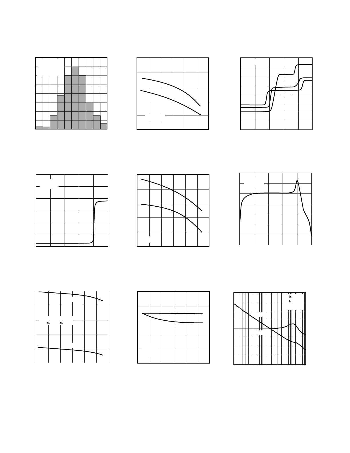
Figure 1. Input Offset Distribution
2.5
1.50.5–0.5–1.5
90
80
–I
SC
70
+I
60
VS = +5V
50
V
SHORT CIRCUIT CURRENT – mA
CM
40
–25
–50
SC
= +2.5V
TEMPERATURE – 8C
7550250
Figure 2. Short Circuit Current vs.
Temperature
100
Figure 3. Input Bias Current
vs. Common-Mode Voltage
3.0
VS = +5V
2.5
T
= +258C
A
2.0
1.5
1.0
OFFSET VOLTAGE – mV
0.5
0
1
0
COMMON-MODE VOLTAGE – Volts
Figure 4. Offset Voltage vs.
Common-Mode Voltage
1000
RL= 2kV
800
VS = 15V
600
0.3
V
4.7V
OUT
400
OPEN-LOOP GAIN – V/mV
200
0
–25
–50
Figure 7. Open-Loop Gain vs.
Temperature
RL= 1kV
TEMPERATURE – 8C
432
7550250
100
100
–I
90
80
70
60
SHORT CIRCUIT CURRENT – mA
VS = 65V
50
–25
5
–50
Figure 5. Short Circuit Current vs.
Temperature
5
4
3
2
SLEW RATE – V/ms
1
0
–50
VS = +5V
R
= 1kV
L
= +1nF
C
L
–25
Figure 8. Slew Rate vs.
Temperature
SC
+I
SC
TEMPERATURE – 8C
+EDGE
–EDGE
TEMPERATURE – 8C
–4–
100
7550250
Figure 6. Bandwidth vs.
Common-Mode Voltage
100
7550250
Figure 9. Open-Loop Gain and
Phase vs. Frequency
REV. F

OP179/OP279
PHASE
GAIN
120
40
–40
100 1k 10M1M100k10k
60
80
100
–20
0
20
270
90
–90
135
180
225
–45
0
45
FREQUENCY – Hz
OPEN-LOOP GAIN – dB
PHASE – Degrees
VS 62.5V
TA –408C
RL = 2kV
CL = 500pF
80
0
10k
20
10
0
40
30
50
60
70
8k6k4k2k
LOAD CAPACITANCE – pF
OVERSHOOT – %
TA = +258C
A
VCL
= +1
R
L
1kV
VS 62.5V
VIN = +100mV p-p
POSITIVE EDGE AND
NEGATIVE EDGE
6.5
6.0
5.5
5.0
SUPPLY CURRENT – mA
4.5
4.0
–50
VS = 66V
VS = 65V
VS = +5V
V
CM
–25
TEMPERATURE – 8C
= +2.5V
100
7550250
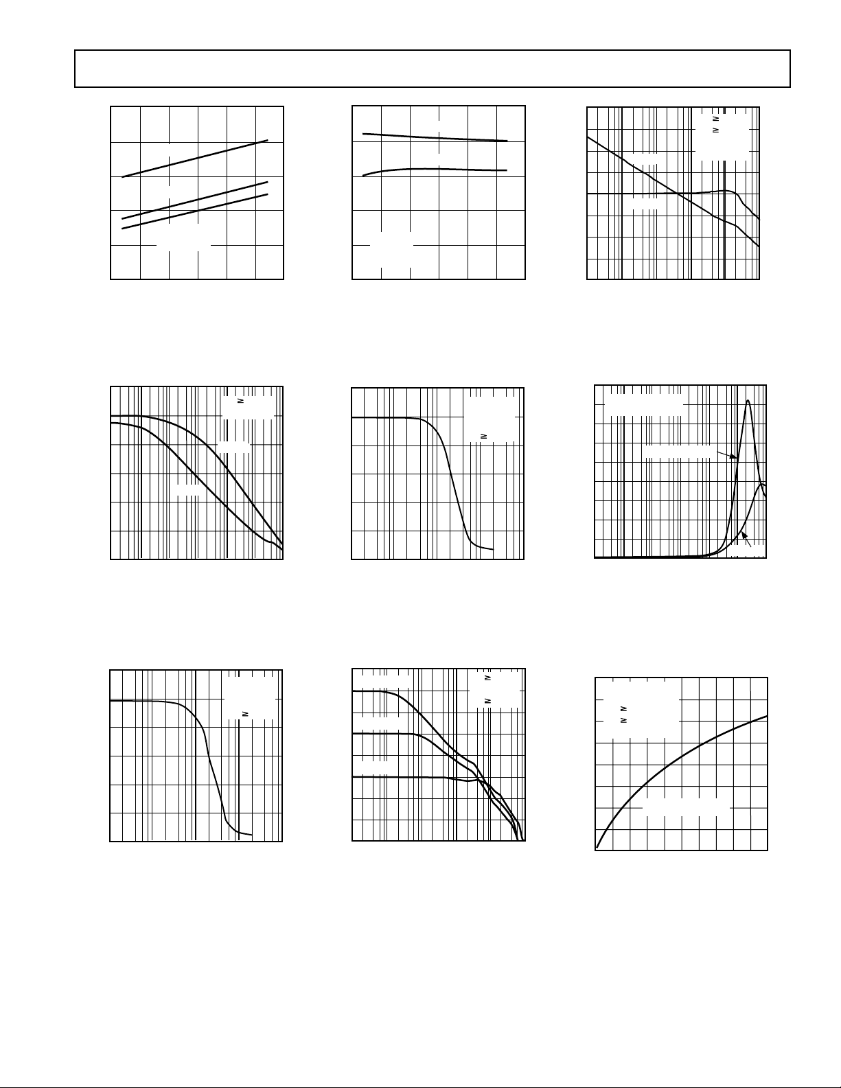
Figure 10. Supply Current vs.
Temperature
120
VS 62.5V
100
80
60
40
20
POWER SUPPLY REJECTION – dB
0
10 100 10M1M100k10k1k
+PSRR
FREQUENCY – Hz
TA = +258C
–PSRR
Figure 13. Power Supply Rejection vs.
Frequency
5
+EDGE
4
–EDGE
3
2
SLEW RATE – V/ms
1
0
–50
VS = 65V
RL = 1kV
C
= +1nF
L
–25
TEMPERATURE – 8C
100
7550250
Figure 11. Slew Rate vs. Temperature
6
TA = +258C
= 62.5V
V
5
4
3
2
1
MAXIMUM OUTPUT SWING – Volts
0
10k
FREQUENCY – Hz
S
A
VCL
R
L
1M100k1k
= +1
1kV
10M
Figure 14. Maximum Output
Swing vs. Frequency
Figure 12. Open-Loop Gain and
Phase vs. Frequency
180
TA = +258C
160
V
= 62.5V OR 65V
S
140
120
100
80
IMPEDANCE – V
60
40
20
0
10 100 10M1M100k10k1k
A
= 10 OR 100
VCL
FREQUENCY – Hz
Figure 15. Closed-Loop Output
Impedance vs. Frequency
A
= 1
VCL
Figure 16. Maximum Output Swing
vs. Frequency
REV. F
12
10
8
6
4
2
MAXIMUM OUTPUT SWING – Volts
0
10k 10M1M100k1k
FREQUENCY – Hz
TA = +258C
= 65V
V
S
= +1
A
VCL
1kV
R
L
50
A
= +100
VCL
40
30
A
= +10
VCL
20
10
A
= +1
VCL
0
–10
CLOSED-LOOP GAIN – dB
–20
–30
1k 10k 100M10M1M100k
FREQUENCY – Hz
VS 62.5V
TA = +258C
RL 1kV
Figure 17. Closed-Loop Gain vs.
Frequency
–5–
Figure 18. Small Signal Overshoot
vs. Load Capacitance
 Loading...