

Low Noise, Precision
–
www.BDTIC.com/ADI
FEATURES
Low noise: 80 nV p-p (0.1 Hz to 10 Hz), 3 nV/√Hz
Low drift: 0.2 μV/°C
High speed: 2.8 V/μs slew rate, 8 MHz gain bandwidth
Low V
Excellent CMRR: 126 dB at VCM of ±11 V
High open-loop gain: 1.8 million
Fits OP07, 5534A sockets
Available in die form
GENERAL DESCRIPTION
The OP27 precision operational amplifier combines the low
offset and drift of the OP07 with both high speed and low noise.
Of
the OP27 ideal for precision instrumentation applications.
Exceptionally low noise, e
noise corner frequency of 2.7 Hz, and high gain (1.8 million),
allow accurate high-gain amplification of low-level signals.
A gain-bandwidth product of 8 MHz and a 2.8 V/μs slew rate
provide excellent dynamic accuracy in high speed, dataacquisition systems.
A low input bias current of ±10 nA is achieved by use of a bias
current cancellation circuit. Over the military temperature
range, this circuit typically holds I
and 15 nA, respectively.
The output stage has good load driving capability. A guaranteed
swin
OP27 an excellent choice for professional audio applications.
: 10 μV
OS
fsets down to 25 μV and maximum drift of 0.6 μV/°C make
= 3.5 nV/√Hz, at 10 Hz, a low 1/f
n
and IOS to ±20 nA
B
g of ±10 V into 600 Ω and low output distortion make the
(Continued on Page 3)
Operational Amplifier
OP27
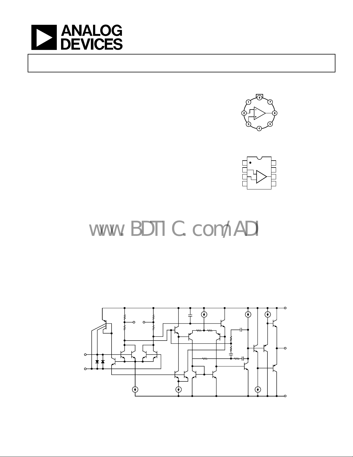
PIN CONFIGURATIONS
BAL
BAL 1
IN 2
+IN 3
OP27
4V– (CASE)
NC = NO CONNECT
Figure 1. 8-Lead TO-99 (J-Suffix)
OS
TRIM
–IN
+IN
1
OP27
2
3
4
NC = NO CONNECT
V
Figure 2. 8-Lead CERDIP – Glass Hermetic Seal (Z-Suffix),
8-Lead
PDIP (P-Suffix),
8-Lead SO (S-Suffix)
V+
OUT
NC
00317-001
8
V
TRIM
OS
7
V+
6
OUT
5
NCV–
00317-002
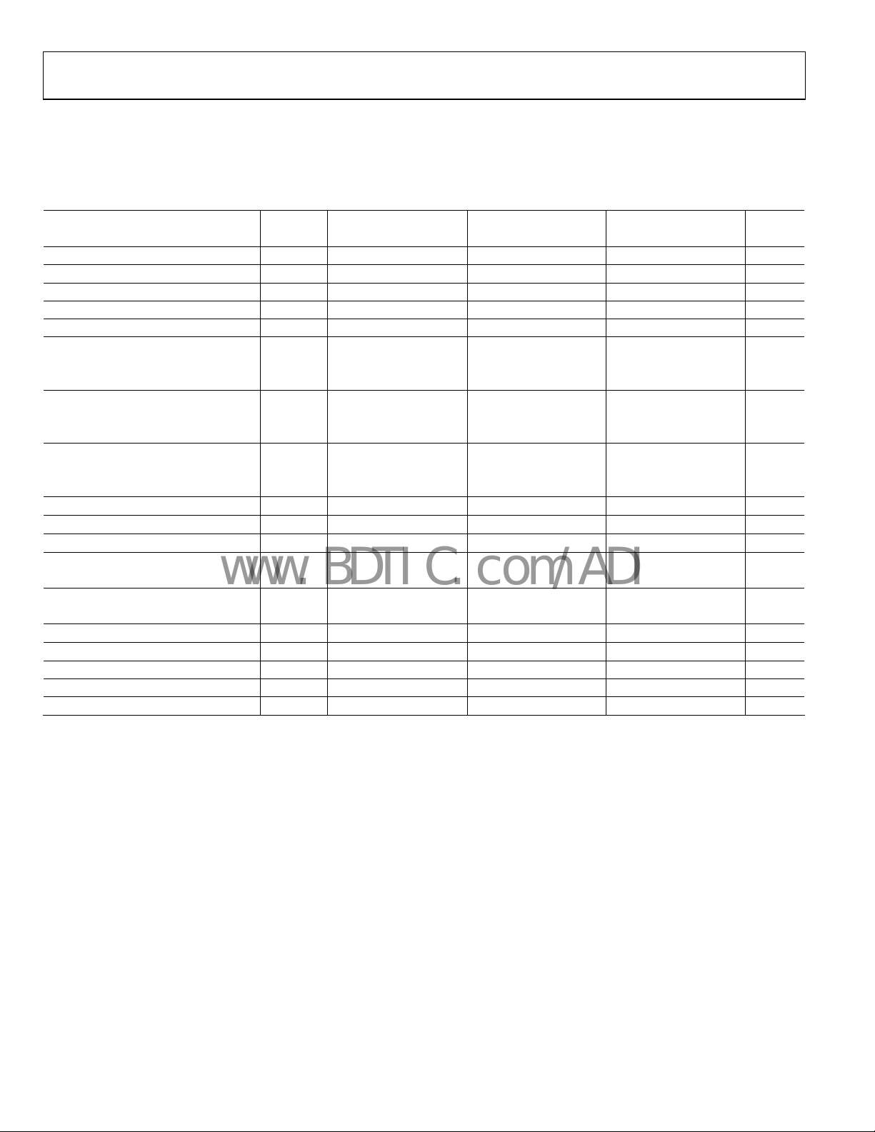
FUNCTIONAL BLOCK DIAGRAM
.
Q2B
R4
1
R2
Q2AQ1A Q1B
Q11 Q12
R3
Q6
NONINVERTING
INPUT (+)
INVERTING
INPUT (–)
1
R1 AND R2 ARE PERMANENTLY
ADJUSTED AT WAFER TEST FOR
MINIMUM OFFSET VOLTAGE
Rev. F
Information furnished by Analog Devices is believed to be accurate and reliable. However, no
responsibility is assumed by Anal og Devices for its use, nor for any infringements of patents or ot her
rights of third parties that may result from its use. Specifications subject to change without notice. No
license is granted by implication or otherwise under any patent or patent rights of Analog Devices.
Trademarks and registered trademarks are the property of their respective owners.
Q3
18
VOS ADJ.
1
R1
V+
C2
Q21
Q23
Q27 Q28
R23 R24
R5
Q24
Q22
C1
R9
R12
C3 C4
Q20 Q19
Q26
Q46
OUTPUT
Q45
V–
Figure 3.
One Technology Way, P.O. Box 9106, Norwood, MA 02062-9106, U.S.A.
Tel: 781.329.4700 www.analog.com
Fax: 781.461.3113 ©2006 Analog Devices, Inc. All rights reserved.
00317-003

OP27
www.BDTIC.com/ADI
TABLE OF CONTENTS
Features.............................................................................................. 1
Typical Performance Characteristics..............................................8
General Description......................................................................... 1
Pin Configurations........................................................................... 1
Functional Block Diagram ..............................................................1
Revision History ...............................................................................2
Specifications..................................................................................... 4
Electrical Characteristics............................................................. 4
Typical Electrical Characteristics ...............................................6
Absolute Maximum Ratings............................................................ 7
Thermal Resistance...................................................................... 7
ESD Caution.................................................................................. 7
REVISION HISTORY
5/06—Rev. E to Rev. F
Removed References to 745 ..............................................Universal
Updated 741 to AD741......................................................Universal
Changes to Ordering Guide.......................................................... 20
12/05—Rev. D to Rev. E
E
dits to Figure 2................................................................................ 1
9/05—Rev. C to Rev. D
pdated Format..................................................................Universal
U
Changes to Table 1............................................................................ 4
Removed Die Characteristics Figure ............................................ 5
Removed Wafer Test Limits Table .................................................. 5
Changes to Table 5............................................................................ 7
Changes to Comments on Noise Section ....................................15
Changes to Ordering Guide.......................................................... 24
Application Information................................................................ 14
Offset Voltage Adjustment........................................................ 14
Noise Measurements.................................................................. 14
Unity-Gain Buffer Applications ............................................... 14
Comments On Noise................................................................. 15
Audio Applications .................................................................... 16
References.................................................................................... 18
Outline Dimensions....................................................................... 19
Ordering Guide............................................................................... 20
9/01—Rev. 0 to Rev. A
dits to Ordering Information ........................................................1
E
Edits to Pin Connections..................................................................1
Edits to Absolute Maximum Ratings ..............................................2
Edits to Package Type .......................................................................2
Edits to Electrical Characteristics .............................................. 2, 3
Edits to Wafer Test Limits ................................................................4
Deleted Typical Electrical Characteristics......................................4
Edits to Burn-In Circuit Figure.......................................................7
Edits to Application Information ....................................................8
1/03—Rev. B to Rev. C
E
dits to Pin Connections................................................................. 1
Edits to General Description........................................................... 1
Edits to Die Characteristics............................................................. 5
Edits to Absolute Maximum Ratings ............................................. 7
Updated Outline Dimensions....................................................... 16
Edits to Figure 8.............................................................................. 14
Edits to Outline Dimensions......................................................... 16
Rev. F | Page 2 of 20

OP27
www.BDTIC.com/ADI
GENERAL DESCRIPTION
(Continued from Page 1)
PSRR and CMRR exceed 120 dB. These characteristics, coupled
th long-term drift of 0.2 μV/month, allow the circuit designer
wi
to achieve performance levels previously attained only by
discrete designs.
Low cost, high volume production of OP27 is achieved by
usin
g an on-chip Zener zap-trimming network. This reliable
and stable offset trimming scheme has proven its effectiveness
over many years of production history.
The OP27 provides excellent performance in low noise,
h accuracy amplification of low level signals. Applications
hig
include stable integrators, precision summing amplifiers,
precision voltage threshold detectors, comparators, and
professional audio circuits such as tape heads and microphone preamplifiers.
The OP27 is a direct replacement for OP06, OP07, and OP45
a
mplifiers; AD741 types can be directly replaced by removing
he nulling potentiometer of the AD741.
t
Rev. F | Page 3 of 20
OP27
www.BDTIC.com/ADI
SPECIFICATIONS
ELECTRICAL CHARACTERISTICS
VS = ±15 V, TA = 25°C, unless otherwise noted.
Table 1.
OP27A/E OP27/G
Parameter Symbol Conditions Min Typ Max Min Typ Max Unit
INPUT OFFSET VOLTAGE
LONG-TE RM VOS STABILITY2,
INPUT OFFSET CURRENT IOS 7 35 12 75 nA
INPUT BIAS CURRENT IB ±10 ±40 ±15 ±80 nA
INPUT NOISE VOLTAGE
INPUT NOISE en fO = 10 Hz 3.5 5.5 3.8 8.0 nV/√Hz
Voltage Density
f
INPUT NOISE in fO = 10 Hz 1.7 4.0 1.7 pA/√Hz
Current Density
INPUT RESISTANCE
Differential Mode
Common Mode R
INPUT VOLTAGE RANGE IVR ±11.0 ±12.3
COMMON-MODE REJECTION RATIO CMRR VCM = ±11 V 114 126
POWER SUPPLY REJECTION RATIO PSRR VS = ±4 V to ±18 V
LARGE SIGNAL VOLTAGE GAIN AVO RL ≥ 2 k Ω, VO = ±10 V 1000 1800
OUTPUT VOLTAGE SWING VO RL ≥ 2 k Ω ±12.0 ±13.8
SLEW RATE
6
GAIN BANDWIDTH PRODUCT
OPEN-LOOP OUTPUT RESISTANCE RO VO = 0, IO = 0 70 70 Ω
POWER CONSUMPTION Pd VO 90 140 100 170 mW
OFFSET ADJUSTMENT RANGE RP = 10 kΩ ±4.0
1
Input offset voltage measurements are performed approximately 0.5 seconds after application of power. A/E grades guaranteed fully warmed up.
2
Long-term input offset voltage stability refers to the average trend line of VOS vs. time over extended periods after the first 30 days of operation. Excluding the initial
hour of operation, changes in V
3
Sample tested.
4
See voltage noise test circuit (Figure 31).
5
Guaranteed by input bias current.
6
Guaranteed by design.
1
3
3, 4
3
3
5
6
during the first 30 days are typically 2.5 μV. Refer to the Typical Performance Characteristics section.
OS
VOS 10 25 30 100 μV
VOS/Time 0.2 1.0 0.4 2.0 μV/MO
e
0.1 Hz to 10 Hz 0.08 0.18 0.09 0.25 μV p-p
n p-p
f
RIN 1.3 6
INCM
SR RL ≥ 2 kΩ 1.7 2.8
GBW 5.0 8.0
= 30 Hz 3.1 4.5 3.3 5.6 nV/√Hz
O
= 1000 Hz 3.0 3.8 3.2 4.5 nV/√Hz
O
= 30 Hz
f
O
fO = 1000 Hz
≥ 600 Ω, VO = ±10 V 800 1500
R
L
≥ 600 Ω ±10.0 ±11.5
R
L
1.0 2.3
0.4 0.6
3
0.7 4
±11.0 ±12.3
100 120
1.0
pA/√Hz
0.4 0.6 pA/√Hz
MΩ
2
GΩ
V
dB
1 10 2 20 μV/V
700 1500
600 1500
±11.5 ±13.5
±10.0 ±11.5
1.7 2.8
5.0 8.0
±4.0
V/mV
V/mV
V
V
V/μs
MHz
mV
Rev. F | Page 4 of 20
OP27
www.BDTIC.com/ADI
VS = ±15 V, −55°C ≤ TA ≤ 125°C, unless otherwise noted.
Table 2.
OP27A
Parameter Symbol Conditions Min Typ Max Unit
INPUT OFFSET VOLTAGE
AVERAGE INPUT OFFSET DRIFT TCV
INPUT OFFSET CURRENT IOS 15 50 nA
INPUT BIAS CURRENT IB ±20 ±60 nA
INPUT VOLTAGE RANGE IVR ±10.3 ±11.5 V
COMMON-MODE REJECTION RATIO CMRR VCM = ±10 V 108 122
POWER SUPPLY REJECTION RATIO PSRR VS = ±4.5 V to ±18 V 2 16 μV/V
LARGE SIGNAL VOLTAGE GAIN AVO RL ≥ 2 kΩ, VO = ±10 V 600 1200
OUTPUT VOLTAGE SWING VO RL ≥ 2 kΩ ±11.5 ±13.5
1
Input offset voltage measurements are performed by automated test equipment approximately 0.5 seconds after application of power. A/E grades guaranteed fully
warmed up.
2
The TCVOS performance is within the specifications unnulled or when nulled with RP = 8 kΩ to 20 kΩ. TCVOS is 100% tested for A/E grades, sample tested for G grades.
3
Guaranteed by design.
VS = ±15 V, −25°C ≤ TA ≤ 85°C for OP27J, OP27Z, 0°C ≤ TA ≤ 70°C for OP27EP, and –40°C ≤ TA ≤ 85°C for OP27GP, OP27GS, unless
otherwise noted.
Table 3.
OP27E OP27G
Parameter Symbol Conditions Min Typ Max Min Typ Max Unit
INPUT ONSET VOLTAGE VOS
AVERAGE INPUT OFFSET DRIFT TCV
INPUT OFFSET CURRENT IOS
INPUT BIAS CURRENT IB
INPUT VOLTAGE RANGE IVR ±10.5 ±11.8
COMMON-MODE REJECTION RATIO CMRR VCM = ±10 V 110 124
POWER SUPPLY REJECTION RATIO PSRR VS = ±4.5 V to ±18 V 2 15 2 32 μV/V
LARGE SIGNAL VOLTAGE GAIN AVO RL ≥ 2 kΩ, VO = ±10 V 750 1500
OUTPUT VOLTAGE SWING VO RL ≥ 2 kΩ ±11.7 ±13.6
1
The TCVOS performance is within the specifications unnulled or when nulled with RP = 8 kΩ to 20 kΩ. TCVOS is 100% tested for A/E grades, sample tested for C/G grades.
2
Guaranteed by design.
1
TCV
VOS 30 60 μV
OS
OSn
1
2
TCV
2
OS
3
OSn
0.2 0.6 μV/°C
20 50
0.2 0.6
0.2 0.6
10 50
±14 ±60
±10.5 ±11.8
96 118
450 1000
±11.0 ±13.3
55 220 μV
0 4 1.8 μV/°C
0 4 1.8 μV/°C
20 135 nA
±25 ±150 nA
dB
V/mV
V
V
dB
V/mV
V
Rev. F | Page 5 of 20
OP27
www.BDTIC.com/ADI
TYPICAL ELECTRICAL CHARACTERISTICS
VS = ±15 V, TA = 25°C unless otherwise noted.
Table 4.
Parameter Symbol Conditions OP27N Typical Unit
AVERAGE INPUT OFFSET VOLTAGE DRIFT
TCV
AVERAGE INPUT OFFSET CURRENT DRIFT TCIOS 80 pA/°C
AVERAGE INPUT BIAS CURRENT DRIFT TCIB 100 pA/°C
INPUT NOISE VOLTAGE DENSITY en fO = 10 Hz 3.5 nV/√Hz
e
e
INPUT NOISE CURRENT DENSITY in fO = 10 Hz 1.7 pA/√Hz
i
i
INPUT NOISE VOLTAGE SLEW RATE e
GAIN BANDWIDTH PRODUCT GBW 8 MHz
1
Input offset voltage measurements are performed by automated test equipment approximately 0.5 seconds after application of power.
1
TCVOS or Nulled or unnulled 0.2 μV/°C
RP = 8 kΩ to 20 kΩ
OSn
fO = 30 Hz 3.1 nV/√Hz
n
fO = 1000 Hz 3.0 nV/√Hz
n
fO = 30 Hz 1.0 pA/√Hz
n
fO = 1000 Hz 0.4 pA/√Hz
n
0.1 Hz to 10 Hz 0.08 μV p-p
np-p
SR R
≥ 2 kΩ 2.8 V/μs
L
Rev. F | Page 6 of 20

OP27
www.BDTIC.com/ADI
ABSOLUTE MAXIMUM RATINGS
Table 5.
Parameter Rating
Supply Voltage ±22 V
Input Voltage
Output Short-Circuit Duration Indefinite
Differential Input Voltage
Differential Input Current
Storage Temperature Range −65°C to +150°C
Operating Temperature Range
OP27A (J, Z) −55°C to +125°C
OP27E, ( Z) −25°C to +85°C
OP27E, (P) 0°C to 70°C
OP27G (P, S, J, Z) −40°C to +85°C
Lead Temperature Range (Soldering, 60 sec) 300°C
Junction Temperature −65°C to +150°C
1
For supply voltages less than ±22 V, the absolute maximum input voltage is
equal to the supply voltage.
2
The inputs of the OP27 are protected by back-to-back diodes. Current
limiting resistors are not used in order to achieve low noise. If differential
input voltage exceeds ±0.7 V, the input current should be limited to 25 mA.
1
2
2
±22 V
±0.7 V
±25 mA
Stresses above those listed under Absolute Maximum Ratings
may cause permanent damage to the device. This is a stress
rating only; functional operation of the device at these or any
other conditions above those indicated in the operational
section of this specification is not implied. Exposure to absolute
maximum rating conditions for extended periods may affect
device reliability.
THERMAL RESISTANCE
θJA is specified for the worst-case conditions, that is, θ
specified for device in socket for TO, CERDIP, and PDIP
packages; θ
is specified for device soldered to printed circuit
JA
board for SO package.
Absolute maximum ratings apply to both DICE and packaged
arts, unless otherwise noted.
p
Table 6.
Package Type θJA θ
TO-99 (J) 150 18 °C/W
8-Lead Hermetic DlP (Z) 148 16 °C/W
8-Lead Plastic DIP (P) 103 43 °C/W
8-Lead SO (S) 158 43 °C/W
JC
is
JA
Unit
ESD CAUTION
ESD (electrostatic discharge) sensitive device. Electrostatic charges as high as 4000 V readily accumulate on
the human body and test equipment and can discharge without detection. Although this product features
proprietary ESD protection circuitry, permanent damage may occur on devices subjected to high energy
electrostatic discharges. Therefore, proper ESD precautions are recommended to avoid performance
degradation or loss of functionality.
Rev. F | Page 7 of 20

OP27
www.BDTIC.com/ADI
TYPICAL PERFORMANCE CHARACTERISTICS
100
90
10
TA = 25°C
V
= ±15V
S
80
70
60
GAIN (dB)
50
TEST TIME OF 10sec FURTHER
LIMITS LOW FREQUENCY
40
(<0.1Hz) GAIN
30
0.01 0.1 1 10 100
Figure 4. 0.1 Hz to 10 Hz p-p Noise Tes
10
9
8
7
6
5
4
3
I/F CORNER = 2.7Hz
2
VOLTAGE NOISE (nV/√Hz)
1
1 10 100 1k
FREQUENCY (Hz)
ter Frequency Response
FREQUENCY (Hz)
Figure 5. Voltage Noise Density vs. Frequency
TA = 25°C
= ±15V
V
S
00317-004
00317-005
1
0.1
RMS VOLTAGE NOISE (μV)
0.01
100 1k 10k 100k
BANDWIDTH (Hz)
00317-007
Figure 7. Input Wideband Voltage Noise vs. Bandwidth (0.1 Hz to Frequency
Indicated)
100
TA = 25°C
V
= ±15V
S
10
AT 10Hz
TOTAL NOISE (nV/√Hz)
AT 1kHz
RESISTOR NOISE ONLY
1
100 1k 10k
SOURCE RESISTANCE (Ω)
R1
R2
R
– 2R1
S
00317-008
Figure 8. Total Noise vs. Sourced Resistance
100
741
10
I/F CORNER = 2.7Hz
VOLTAGE NOISE (nV/√Hz)
INSTRUMENTATION
1
1 10 100 1k
I/F CORNER
OP27 I/F CORNER
RANGE TO DC
FREQUENCY (Hz)
LOW NOISE
AUDIO OP AMP
AUDIO RANGE
TO 20kHz
00317-006
Figure 6. A Comparison of Op Amp Voltage Noise Spectra
Rev. F | Page 8 of 20
5
4
AT 10Hz
3
AT 1kHz
VOLTAGE NOISE (nV/√Hz)
2
1
–50 0–25 100755025 125
TEMPERATURE (°C)
Figure 9. Voltage Noise Density vs. Temperature
VS = ±15V
00317-009

OP27
www.BDTIC.com/ADI
5
TA = 25°C
4
3
VOLTAGE NOISE (nV/√Hz)
2
1
04
10 20 30
TOTAL SUPPLY VOLTAGE, V+ – V–, (V)
AT 10Hz
AT 1kHz
0
00317-010
Figure 10. Voltage Noise Density vs. Supply Voltage
60
50
40
30
20
10
0
–10
–20
–30
OFFSET VOLTAGE (μV)
–40
TRIMMING WITH
–50
10kΩ POT DOES
NOT CHANGE
–60
TCV
OS
–70
–50 –25 0 25 50 75 100 125 150
–75 175
Figure 13. Offset Voltage Drift of Five
TEMPERATURE (°C)
Representative Units vs. Temperature
OP27C
OP27A
OP27A
OP27A
OP27C
00317-013
10.0
Hz)
√
1.0
CURRENT NOISE (pA/
I/F CORNER = 140Hz
0.1
10 10k
100 1k
FREQUENCY (Hz)
00317-011
Figure 11. Current Noise Density vs. Frequency
5.0
4.0
TA = +125°C
3.0
TA = –55°C
SUPPLY CURRENT (mA)
2.0
TA = +25°C
1.0
54
15 25 35
TOTAL SUPPLY VOLTAGE (V)
5
00317-012
Figure 12. Supply Current vs. Supply Voltage
6
4
2
0
–2
–4
–6
6
4
2
0
CHANGE IN OFFSET VOLTAGE (μV)
–2
–4
–6
07
123456
Figure 14. Long-Term Offset Voltage D
TA= 25°C
= 15V
V
S
10
5
CHANGE IN INPUT OFFSET VOLTAGE (μV)
1
0
Figure 15. Warm-Up Offset Voltage Drift
TIME (Months)
rift of Six Representative Units
OP27 C/G
OP27 F
OP27 A/E
1234
TIME AFTER POWER ON (Min)
5
00317-014
00317-015
Rev. F | Page 9 of 20

OP27
www.BDTIC.com/ADI
OPEN-LOOP GAIN (dB)
30
25
TA =
°
C
25
20
15
10
5
0
–20 100
= 70°C
T
A
THERMAL
SHOCK
RESPONSE
BAND
DEVICE IMMERSED
IN 70
°
C OIL BATH
0 20406080
TIME (Sec)
VS =±15V
Figure 16. Offset Voltage Change Due to Thermal Shock
00317-016
130
110
90
70
50
VOLTAGE GAIN (dB)
30
10
–10
10 1001 1k 10k 100k 1M 10M
FREQUENCY (Hz)
100M
00317-019
Figure 19. Open-Loop Gain vs. Frequency
50
40
30
20
INPUT BIAS CURRENT (nA)
10
0
–50 –25 0 25 50 75 100 125
TEMPERATURE (
OP27C
OP27A
Figure 17. Input Bias Current vs. Temperature
50
40
30
20
INPUT OFFSET CURRENT (nA)
10
0
–50 –25–75 0 25 50 75 100
TEMPERATURE (
OP27C
OP27A
Figure 18. Input Offset Current vs. Temperature
125
10
9
8
7
6
GAIN BANDWIDTH PRODUCT (MHz)
00317-020
VS=±15V
150
°
C)
00317-017
70
60
50
4
3
SLEW RATE (V/μS) PHASE MARGIN (Degrees)
2
–50 –25–75 0 25 50 75 100
TEMPERATURE (°C)
Figure 20. Slew Rate, Gain Bandwidt
ΦM
VS= ±15V
GBW
SLEW
h Product, Phase Margin vs.
Temperature
= ±15V
100M
80
100
120
140
160
180
200
220
PHASE SHIFT (Degrees)
00317-021
VS=±15V
125
°
C)
00317-018
25
20
GAIN
15
PHASE
10
5
GAIN (dB)
0
–5
–10
1M
MARGIN
= 70°
10M
FREQUENCY (Hz)
TA = 25°C
V
S
Figure 21. Gain, Phase Shift vs. Frequency
Rev. F | Page 10 of 20

OP27
–
www.BDTIC.com/ADI
2.5
TA= 25°C
2.0
RL= 2kΩ
1.5
RL= 1kΩ
1.0
OPEN-LOOP GAIN (V/μV)
0.5
% OVERSHOOT
100
VS= ±15V
V
= 100mV
IN
A
= +1
80
60
40
20
V
0
050
Figure 22. Open-Loop Voltage
28
24
20
16
12
8
MAXIMUM OUTPUT SWING
4
0
1k 10M
10 20 30 40
TOTAL SUPPLY VOLTAGE (V)
Gain vs. Supply Voltage
10k 100k 1M
FREQUENCY (Hz)
TA= 25°C
V
= ±15V
S
00317-022
00317-023
Figure 23. Maximum Output Swing vs. Frequency
18
16
14
12
10
8
6
4
MAXIMUM OUTPUT (V)
2
0
–2
100
POSITIVE
SWING
LOAD RESISTANCE (
NEGATIVE
SWING
1k
TA= 25°C
V
=±15V
S
Ω
)
10k
00317-024
Figure 24. Maximum Output Voltage vs. Load Resistance
0
0 2500
500 1000 1500 2000
Figure 25. Small-Signal Overshoot vs. Capacitive Load
20mV 500ns
50mV
0V
50mV
Figure 26. Small-Signal Transient Response
2V 2μs
+5V
0V
–5V
Figure 27. Large Signal Transient Response
CAPACITIVE LOAD (pF)
A
C
V
T
A
VCL
V
S
T
A
= +1
VCL
= 15pF
L
= ±15V
S
= 25°C
A
= +1
= ±15V
= 25°C
00317-025
00317-026
00317-027
Rev. F | Page 11 of 20

OP27
www.BDTIC.com/ADI
SHORT-CIRCUIT CURRENT (mA)
60
50
40
30
20
TA= 25°C
V
= 15V
S
ISC(+)
ISC(–)
10
0.1μF
100k
Ω
Ω
OP27
D.U.T.
VOLTAGE
GAIN
= 50,000
4.7μF
Ω
2k
22μF
4.3k
OP12
100k
Ω
SCOPE× 1
= 1M
Ω
R
Ω
IN
10
05
140
120
100
CMRR (dB)
80
60
100 1M
16
12
8
4
0
–4
–8
COMMON-MODE RANGE (V)
–12
–16
0
Figure 30. Common-Mode Input R
1234
TIME FROM OUTPUT SHORTED TO GROUND (Min)
Figure 28. Short-Circuit Current vs. Time
VS= ±15V
T
= 25°C
A
V
CM
1k 10k 100k
FREQUENCY (Hz)
Figure 29. CMRR vs. Frequency
TA = –55°C
TA = +25°C
TA = +125°C
TA = –55°C
TA = +25°C
TA = +125°C
±5 ±10 ±15
SUPPLY VOLTAGE (V)
ange vs. Supply Voltage
= ±10V
±20
00317-028
00317-029
00317-030
Figure 31. Voltage Noise Test Circuit (0.1 Hz to 10 Hz)
2.4
TA = 25°C
V
= ±15V2.2
S
2.0
1.8
1.6
1.4
1.2
1.0
0.8
OPEN-LOOP VOLTAGE GAIN (V/μV)
0.6
0.4
100 1k 10k 100k
Figure 32. Open-Loop Voltage Gain vs. Load Resistance
120
80
40
0
–40
VOLTAGE NOISE (nV)
–90
–120
2.2μF
0.1μF
24.3k
Ω
LOAD RESISTANCE (Ω)
1 SEC/DIV
0.1Hz TO 10Hz p-p NOISE
Figure 33. Low Frequency Noise
110k
Ω
00317-031
00317-032
00317-033
Rev. F | Page 12 of 20

OP27
www.BDTIC.com/ADI
160
140
120
100
80
60
40
20
POWER SUPPLY REJECTION RATIO (dB)
TA = 25°C
NEGATIVE
SWING
POSITIVE
SWING
0
1 100M
10 100 1k 10k 100k 1M 10M
FREQUENCY (Hz)
Figure 34. PSRR vs. Frequency
00317-034
Rev. F | Page 13 of 20

OP27
www.BDTIC.com/ADI
APPLICATION INFORMATION
OP27 series units can be inserted directly into OP07 sockets
with or without removal of external compensation or nulling
components. Additionally, the OP27 can be fitted to unnulled
AD741-type sockets; however, if conventional AD741 nulling
cuitry is in use, it should be modified or removed to ensure
cir
correct OP27 operation. OP27 offset voltage can be nulled to
0 (or another desired setting) using a potentiometer (see
35).
Figure
The OP27 provides stable operation with load capacitances of
p to 2000 pF and ±10 V swings; larger capacitances should be
u
decoupled with a 50 Ω resistor inside the feedback loop. The
OP27 is unity-gain stable.
Thermoelectric voltages generated by dissimilar metals at the
put terminal contacts can degrade the drift performance.
in
Best operation is obtained when both input contacts are
maintained at the same temperature.
R
10kΩ
P
1
2
3
OP27
V–
8
7
4
–-
+
Figure 35. Offset Nulling Circuit
V+
6
OUTPUT
00317-035
OFFSET VOLTAGE ADJUSTMENT
The input offset voltage of the OP27 is trimmed at wafer level.
However, if further adjustment of V
potentiometer can be used. TCV
Other potentiometer values from 1 kΩ to 1 MΩ can be used
with a slight degradation (0.1 μV/°C to 0.2 μV/°C) of TCV
Trimming to a value other than zero creates a drift of approximately (V
0.33 μV/°C if V
/300) μV/°C. For example, the change in TCVOS is
OS
is adjusted to 100 μV. The offset voltage
OS
adjustment range with a 10 kΩ potentiometer is ±4 mV. If smaller
adjustment range is required, the nulling sensitivity can be
reduced by using a smaller potentiometer in conjunction with
fixed resistors. For example,
a 280 μV ad
justment range.
1
Figure 36. Offset Voltage Adjustment
is necessary, a 10 kΩ trim
OS
is not degraded (see Figure 35).
OS
Figure 36 shows a network that has
84.7kΩ4.7kΩ 1kΩ POTT
V+
00317-036
.
OS
Rev. F | Page 14 of 20
NOISE MEASUREMENTS
To measure the 80 nV p-p noise specification of the OP27 in
the 0.1 Hz to 10 Hz range, the following precautions must be
observed:
• T
he device must be warmed up for at least five minutes.
As shown in the warm-up drift curve, the offset voltage
typically changes 4 μV due to increasing chip temperature
after power-up. In the 10-second measurement interval,
these temperature-induced effects can exceed tens-ofnanovolts.
or similar reasons, the device has to be well-shielded
• F
from air currents. Shielding minimizes thermocouple effects.
udden motion in the vicinity of the device can also
• S
feedthrough to increase the observed noise.
• The t
est time to measure 0.1 Hz to 10 Hz noise should not
exceed 10 seconds. As shown in the noise-tester frequency
response curve, the 0.1 Hz corner is defined by only one
zero. The test time of 10 seconds acts as an additional zero
to eliminate noise contributions from the frequency band
below 0.1 Hz.
• A n
oise voltage density test is recommended when
measuring noise on a large number of units. A 10 Hz noise
voltage density measurement correlates well with a 0.1 Hz to
10 Hz p-p noise reading, since both results are determined
by the white noise and the location of the 1/f corner
frequency.
UNITY-GAIN BUFFER APPLICATIONS
When Rf ≤ 100 Ω and the input is driven with a fast, large
signal pulse (>1 V), the output waveform looks as shown in the
pulsed operation diagram (see Figure 37).
During the fast feedthrough-like portion of the output, the
put protection diodes effectively short the output to the input,
in
and a current, limited only by the output short-circuit protection, is drawn by the signal generator. With R
output is capable of handling the current requirements (I
at 10 V); the amplifier stays in its active mode and a smooth
transition occurs.
When R
> 2 kΩ, a pole is created with Rf and the amplifier’s
f
input capacitance (8 pF) that creates additional phase shift and
reduces phase margin. A small capacitor (20 pF to 50 pF) in
parallel with R
eliminates this problem.
f
R
f
–
OP27
+
Figure 37. Pulsed Operation
≥ 500 Ω, the
f
≤ 20 mA
L
2.8V/μs
00317-037

OP27
www.BDTIC.com/ADI
COMMENTS ON NOISE
The OP27 is a very low noise, monolithic op amp. The outstanding input voltage noise characteristics of the OP27
are achieved mainly by operating the input stage at a high
quiescent current. The input bias and offset currents, which
would normally increase, are held to reasonable values by the
input bias current cancellation circuit. The OP27A/E has I
and I
of only ±40 nA and 35 nA at 25°C respectively. This
OS
is particularly important when the input has a high source
resistance. In addition, many audio amplifier designers prefer
to use direct coupling. The high I
, VOS, and TCVOS of previous
B
designs have made direct coupling difficult, if not impossible,
to use.
Voltage noise is inversely proportional to the square root of bias
urrent, but current noise is proportional to the square root of
c
bias current. The noise advantage of the OP27 disappears when
high source resistors are used.
mpare the observed total noise of the OP27 with the noise
co
p
erformance of other devices in different circuit applications.
⎡
NoiseTotal
⎢
⎢
=
⎢
⎢
⎣
Figure 38, Figure 39, Figure 40
2
)(
+
NoiseVoltage
RNoiseCurrent
2
)(
NoiseResistor
2/1
⎤
⎥
2
)(
+×
⎥
S
⎥
⎥
⎦
Figure 38 shows noise vs. source resistance at 1000 Hz. The
ame plot applies to wideband noise. To use this plot, multiply
s
the vertical scale by the square root of the bandwidth.
100
50
OP08/108
Hz)
√
TOTAL NOISE (nV/
Figure 38. Noise vs. Source Resistance (Includ
OP07
10
5
5534
OP27/37
REGISTER
1
50 10k
NOISE ONLY
100 50k
500 1k 5k
RS—SOURCE RESISTANCE (Ω)
1 RS UNMATCHED
e.g.R
=RS1 = 10kΩ,RS2 = 0
S
2 R
MATCHED
S
e.g.R
= 10kΩ,RS1 =RS2 = 5k
S
R
R
ing Resistor Noise) at 1000 Hz
S1
S2
At RS < 1 kΩ, the low voltage noise of the OP27 is maintained.
< 1 kΩ, total noise increases but is dominated by the
With R
S
resistor noise rather than current or voltage noise. lt is only
beyond R
of 20 kΩ that current noise starts to dominate. The
S
argument can be made that current noise is not important for
applications with low-to-moderate source resistances. The
crossover between the OP27 and OP07 noise occurs in the 15 kΩ
to 40 kΩ region.
B
1
2
Ω
00317-038
Figure 39 shows the 0.1 Hz to 10 Hz p-p noise. Here the picture
vorable; resistor noise is negligible and current noise
is less fa
becomes important because it is inversely proportional to the
square root of frequency. The crossover with the
n the 3 kΩ to 5 kΩ range depending on whether balanced or
i
unbalanced source resistors are used (at 3 kΩ the I
error also can be 3× the V
1k
OP08/108
500
5534
OP07
100
OP27/37
p-p NOISE (nV)
50
REGISTER
10
50 10k
Figure 39. Peak-to-Peak Noise (0.1 Hz to 10 Hz) as Source Resistance
NOISE ONLY
100 50k
spec).
OS
1
2
1 RS UNMATCHED
e.g.R
=RS1 = 10kΩ,RS2 = 0
S
2 R
MATCHED
S
e.g.R
= 10kΩ,RS1 =RS2 = 5k
S
500 1k 5k
RS—SOURCE RESISTANCE (Ω)
udes Resistor Noise)
(Incl
R
S1
R
S2
OP07 occurs
and IOS
B
Ω
00317-039
For low frequency applications, the OP07 is better than the
OP27/OP37 when RS > 3 kΩ. The only exception is when gain
ror is important.
er
Figure 40 illustrates the 10 Hz noise. As expected, the results are
ween the previous two figures.
bet
100
50
OP08/108
Hz)
√
OP07
10
5534
5
TOTAL NOISE (nV/
OP27/37
REGISTER
1
50 10k
NOISE ONLY
100 50k
500 1k 5k
RS—SOURCE RESISTANCE (Ω)
1 RS UNMATCHED
=RS1 = 10kΩ,RS2 = 0
e.g.R
S
MATCHED
2 R
S
= 10kΩ,RS1 =RS2 = 5k
e.g.R
S
Figure 40. 10 Hz Noise vs. Source Resistance (Includes Resistor Noise)
Audio Applications
1
2
R
S1
R
S2
Ω
00317-040
Rev. F | Page 15 of 20

OP27
C
www.BDTIC.com/ADI
For reference, typical source resistances of some signal sources
are listed in Table 7 .
Table 7.
Source
Device
Impedanc
Strain Gauge <500 Ω
Magnetic
<1500 Ω
Tape Head
e
Comments
Typically used in low frequency
plications.
ap
Low is very important to reduce
self-magnetization problems
when direct coupling is used.
OP27 IB can be neglected.
Magnetic
Phonograph
Cartridges
<1500 Ω
Similar need for low IB in direct
coupled applications. OP27 does
not introduce any selfmagnetization problems.
Linear
Variable
Differential
<1500 Ω
Used in rugged servo-feedback
applications. Bandwidth of
interest is 400 Hz to 5 kHz.
Transform er
Table 8. Open-Loop Gain
Frequency OP07 OP27 OP37
@ 3 Hz 100 dB 124 dB 125 dB
@ 10 Hz 100 dB 120 dB 125 dB
@ 30 Hz 90 dB 110 dB 124 dB
AUDIO APPLICATIONS
Figure 41 is an example of a phono pre-amplifier circuit using the
OP27 for A1; R1-R2-C1-C2 form a very accurate RIAA network
with standard component values. The popular method to
accomplish RIAA phono equalization is to employ frequency
dependent feedback around a high quality gain block. Properly
chosen, an RC network can provide the three necessary time
constants of 3180 μs, 318 μs, and 75 μs.
For initial equalization accuracy and stability, precision metal
ilm resistors and film capacitors of polystyrene or polypro-
f
pylene are recommended because they have low voltage
coefficients, dissipation factors, and dielectric absorption.
(high-k ceramic capacitors should be avoided here, though
low-k ceramics, such as NPO types that have excellent
dissipation factors and somewhat lower dielectric absorption,
can be considered for small values.)
MOVING MAGNET
ARTRIDGE I NPUT
R
A
47.5kΩ
3
C
150pF
A1
A
OP27
2
Figure 41. Phono Preamplifier Circuit
6
C3
0.47µF
R1
97.6kΩ
R2
7.87kΩ
R3
100Ω
G = 1kHz GAIN
= 0.101 ( 1 + )
= 98.677 (39.9dB) AS SHOWN
C4 (2)
220µF
++
LF ROLLOFF
C1
0.03µF
C2
0.01µF
OUT IN
R4
75kΩ
R1
R3
R5
100kΩ
OUTPUT
The OP27 brings a 3.2 nV/√Hz voltage noise and 0.45 pA/√Hz
current noise to this circuit. To minimize noise from other
sources, R3 is set to a value of 100 Ω, generating a voltage noise
of 1.3 nV/√Hz. The noise increases the 3.2 nV/√Hz of the
amplifier by only 0.7 dB. With a 1 kΩ source, the circuit noise
measures 63 dB below a 1 mV reference level, unweighted, in a
20 kHz noise bandwidth.
Gain (G) of the circuit at 1 kHz can be calculated by the
ression:
exp
R1
G 1101.0
⎛
⎜
⎝
⎞
+=
⎟
R3
⎠
For the values shown, the gain is just under 100 (or 40 dB).
Lo
wer gains can be accommodated by increasing R3, but gains
higher than 40 dB show more equalization errors because of the
8 MHz gain bandwidth of the OP27.
This circuit is capable of very low distortion over its entire
ra
nge, generally below 0.01% at levels up to 7 V rms. At 3 V
output levels, it produces less than 0.03% total harmonic
distortion at frequencies up to 20 kHz.
Capacitor C3 and Resistor R4 form a simple −6 dB per octave
umble filter, with a corner at 22 Hz. As an option, the switch
r
selected Shunt Capacitor C4, a nonpolarized electrolytic,
bypasses the low frequency roll-off. Placing the rumble filter’s
high-pass action after the preamplifier has the desirable result
of discriminating against the RIAA-amplified low frequency
noise components and pickup produced low frequency
disturbances.
00317-041
Rev. F | Page 16 of 20
A preamplifier for NAB tape playback is similar to an RIAA
phono preamplifier, though more gain is typically demanded,
along with equalization requiring a heavy low frequency boost.
The circuit in Figure 41 can be readily modified for tape use, as
Figure 42.
shown b
y

OP27
www.BDTIC.com/ADI
Noise performance of this circuit is limited more by the Input
Resist
ors R1 and R2 than by the op amp, as R1 and R2 each
generate a 4 nV/√Hz noise, while the op amp generates a
3.2 nV/√Hz noise. The rms sum of these predominant noise
sources is about 6 nV/√Hz, equivalent to 0.9 μV in a 20 kHz
noise bandwidth, or nearly 61 dB below a 1 mV input signal.
Measurements confirm this predicted performance.
R1
1kΩ
R3
316kΩ
C1
5mF
R6
100Ω
TAP E
HEAD
+
OP27
C
R
A
A
10Ω
–
R2
5kΩ
R1
33kΩ
0.01µF
0.47µF
T1 = 3180µs
T2 = 50µs
Figure 42. Tape Head Preamplifier
15kΩ
00317-042
While the tape equalization requirement has a flat high
frequency gain above 3 kHz (T2 = 50 μs), the amplifier need
not be stabilized for unity gain. The decompensated OP37
rovides a greater bandwidth and slew rate. For many applica-
p
tions, the idealized time constants shown can require trimming
of R1 and R2 to optimize frequency response for nonideal tape
head performance and other factors (see the
secti
on).
References
The network values of the configuration yield a 50 dB gain at
Hz, and the dc gain is greater than 70 dB. Thus, the worst-
1 k
case output offset is just over 500 mV. A single 0.47 μF output
capacitor can block this level without affecting the dynamic
range.
The tape head can be coupled directly to the amplifier input,
ause the worst-case bias current of 80 nA with a 400 mH,
bec
100 μ inch head (such as the PRB2H7K) is not troublesome.
Amplifier bias-current transients that can magnetize a head
resent one potential tape head problem. The OP27 and OP37
p
re free of bias current transients upon power-up or power-
a
down. It is always advantageous to control the speed of power
supply rise and fall to eliminate transients.
In addition, the dc resistance of the head should be carefully
co
ntrolled and preferably below 1 kΩ. For this configuration,
the bias current induced offset voltage can be greater than the
100 pV maximum offset if the head resistance is not sufficiently
controlled.
A simple, but effective, fixed gain transformerless microphone
pre
amp (Figure 43) amplifies differential signals from low
im
pedance microphones by 50 dB and has an input impedance
of 2 kΩ. Because of the high working gain of the circuit, an
OP37 helps to preserve bandwidth, which is 110 kHz. As the
OP37 is a decompensated device (minimum stable gain of 5), a
ummy resistor, R
d
, may be necessary if the microphone is to be
p
unplugged. Otherwise, the 100% feedback from the open input
can cause the amplifier to oscillate.
Common-mode input noise rejection will depend upon the
m
atch of the bridge-resistor ratios. Either close tolerance (0.1%)
types should be used, or R4 should be trimmed for best CMRR.
All resistors should be metal film types for best stability and low
noise.
LOW IMPEDANCE
MICROP HONE INP UT
(Z = 50Ω TO 200Ω)
R4
R3
=
R2
R1
R2
1kΩ
R
P
30kΩ
–
OP27/
OP37
+
R4
316kΩ
R7
10kΩ
OUTPUT
Figure 43. Fixed Gain Transformerless Microphone Preamplifier
For applications demanding appreciably lower noise, a high
quality microphone transformer coupled preamplifier (Figure
44) incorporates the internally compensated OP27. T1 is a JE115K-E 150 Ω/15 kΩ tra
nsformer that provides an optimum
source resistance for the OP27 device. The circuit has an overall
gain of 40 dB, the product of the transformer’s voltage setup and
the op amp’s voltage gain.
C2
1800pF
150Ω
SOURCE
R1
121Ω
1
T1
R3
100Ω
R2
1100Ω
2
A1
OP27
3
6
1
T1 – JENSEN JE – 115K – E
JENSEN TRANSFORMERS
OUTPUT
00317-044
Figure 44. High Quality Microphone Transformer Coupled Preamplifier
Gain can be trimmed to other levels, if desired, by adjusting R2
or R1. Because of the low offset voltage of the OP27, the output
offset of this circuit is very low, 1.7 mV or less, for a 40 dB gain.
The typical output blocking capacitor can be eliminated in such
cases, but it is desirable for higher gains to eliminate switching
transients.
+18V
8
2
3
Figure 45. Burn-In Circuit
OP27
–18V
7
6
4
00317-045
00317-043
Rev. F | Page 17 of 20

OP27
www.BDTIC.com/ADI
Capacitor C2 and Resistor R2 form a 2 μs time constant in this
circuit, as recommended for optimum transient response by the
transformer manufacturer. With C2 in use, A1 must have unitygain stability. For situations where the 2 μs time constant is not
necessary, C2 can be deleted, allowing the faster OP37 to be
ployed.
em
A 150 Ω resistor and R1 and R2 gain resistors connected to a
oiseless amplifier generate 220 nV of noise in a 20 kHz
n
bandwidth, or 73 dB below a 1 mV reference level. Any practical
amplifier can only approach this noise level; it can never exceed
it. With the OP27 and T1 specified, the additional noise
degradation is close to 3.6 dB (or −69.5 referenced to 1 mV).
REFERENCES
1. Lipshitz, S. R, “On RIAA Equalization Networks,” JAES,
Vol. 27, June 1979, p. 458–481.
Jung, W. G., IC Op Amp Cookbook, 2nd. Ed., H. W. Sams
2.
and Company, 1980.
Jung, W. G., Audio IC Op Amp Applications, 2nd. Ed., H. W.
3.
Sams and Company, 1978.
4.
Jung, W. G., and Marsh, R. M., “Picking Capacitors,” Audio,
February and March, 1980.
Otala, M., “Feedback-Generated Phase Nonlinearity in
5.
Audio Amplifiers,” London AES Convention, March 1980,
preprint 1976.
6.
Stout, D. F., and Kaufman, M., Handbook of Operational
Amplifier Circuit Design, New York, McGraw-Hill, 1976.
Rev. F | Page 18 of 20
OP27
www.BDTIC.com/ADI
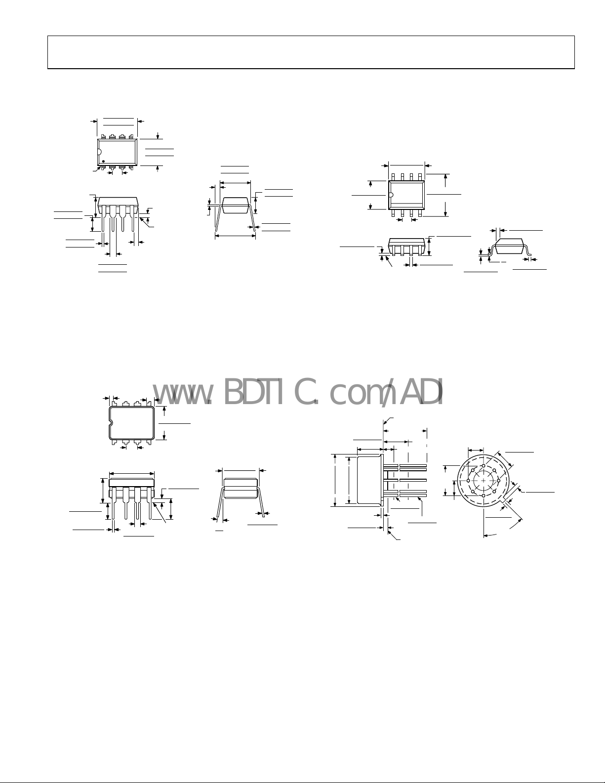
OUTLINE DIMENSIONS
0.400 (10.16)
0.365 (9.27)
0.355 (9.02)
8
5
0.280 (7.11)
4
0.250 (6.35)
0.240 (6.10)
0.015
(0.38)
MIN
SEATING
PLANE
0.005 (0.13)
MIN
(N-8)
P
-Suffix
0.060 (1.52)
0.015 (0.38)
GAUGE
PLANE
MAX
0.325 (8.26)
0.310 (7.87)
0.300 (7.62)
0.430 (10.92)
MAX
0.195 (4.95)
0.130 (3.30)
0.115 (2.92)
0.014 (0.36)
0.010 (0.25)
0.008 (0.20)
5.00 (0.1968)
4.80 (0.1890)
4.00 (0.1574)
3.80 (0.1497)
0.25 (0.0098)
0.10 (0.0040)
COPLANARITY
0.10
CONTROLLING DIMENSIONS ARE IN MILLIMETERS; INCH DIMENSIONS
(IN PARENTHESES) ARE ROUNDED-OFF MILLIMETER EQUIVALENTS FOR
REFERENCE ONLY AND ARE NOT APPROPRIATE FOR USE IN DESIGN.
85
1.27 (0.0500)
SEATING
PLANE
COMPLIANT TO JEDEC STANDARDS MS-012-AA
BSC
6.20 (0.2440)
5.80 (0.2284)
41
1.75 (0.0688)
1.35 (0.0532)
0.51 (0.0201)
0.31 (0.0122)
0.25 (0.0098)
0.17 (0.0067)
0.50 (0.0196)
0.25 (0.0099)
8°
1.27 (0.0500)
0°
0.40 (0.0157)
Figure 48. 8-Lead Standard Small Outline Package [SOIC]
Nar
row Body
(R-8)
S-Suffix
Dimensions shown in millimeters and (inches)
× 45°
1
PIN 1
0.100 (2.54)
0.210
(5.33)
MAX
0.150 (3.81)
0.130 (3.30)
0.115 (2.92)
0.022 (0.56)
0.018 (0.46)
0.014 (0.36)
CONTROLLING DIMENSIONS ARE IN INCHES; MILLIMETER DIMENSIONS
(IN PARENTHESES) ARE ROUNDED-OFF INCH EQUIVALENTS FOR
REFERENCE ONLY AND ARE NOT APPROPRIATE FOR USE IN DESIGN.
CORNER LEADS MAY BE CONFIGURED AS WHOLE OR HALF LEADS.
BSC
0.070 (1.78)
0.060 (1.52)
0.045 (1.14)
COMPLIANT TO JEDEC STANDARDS MS-001-BA
Figure 46. 8-Lead Plastic Dual-in-Line Package [PDIP]
Dimensions shown in inches and (millimeters)
0.005 (0.13)
0.200 (5.08)
MAX
0.200 (5.08)
0.125 (3.18)
0.023 (0.58)
0.014 (0.36)
CONTROLLING DIMENSIONS ARE IN INCHES; MILLIMETER DIMENSIONS
(IN PARENTHESES) ARE ROUNDED-OFF INCH EQUIVALENTS FOR
REFERENCE ONLY AND ARE NOT APPROPRIATE FOR USE IN DESIGN.
0.055 (1.40)
MIN
14
0.100 (2.54) BSC
0.405 (10.29) MAX
MAX
58
0.070 (1.78)
0.030 (0.76)
0.310 (7.87)
0.220 (5.59)
0.060 (1.52)
0.015 (0.38)
0.150 (3.81)
MIN
SEATING
PLANE
0.320 (8.13)
0.290 (7.37)
15°
0°
0.015 (0.38)
0.008 (0.20)
Figure 47. 8-Lead Ceramic DIP – Glass Hermetic Seal [CERDIP]
(Q-8)
Z-Suffi
x
Dimensions shown in inches and (millimeters)
REFERENCE PL ANE
0.5000 (12.70)
0.1850 (4.70)
0.1650 (4.19)
0.3700 (9.40)
0.3350 (8.51)
0.3350 (8.51)
0.3050 (7.75)
0.0400 (1.02) MAX
0.0400 (1.02)
0.0100 (0.25)
CONTROL LING DIM ENSIONS ARE IN INCHES; MILLI METER DIM ENSIONS
(IN PARENT HESES) ARE ROUNDED-OFF INCH EQUIVALENTS FOR
REFERENCE ON LY AND ARE NOT APPROPRI ATE FOR USE IN DE SIGN.
MIN
0.2500 (6.35) MIN
0.0500 (1.27) M AX
0.0190 (0.48)
0.0160 (0.41)
0.0210 (0.53)
0.0160 (0.41)
BASE & SEATING PLANE
COMPLI ANT TO JEDEC STANDARDS MO -002-AK
0.2000
(5.08)
BSC
0.1000
(2.54)
BSC
0.1000 (2.54)
BSC
5
4
3
2
1
0.0340 (0.86)
0.0280 (0.71)
45° BSC
Figure 49. 8-Lead Meta
l Can [TO-99]
0.1600 (4.06)
0.1400 (3.56)
6
7
8
0.0450 (1.14)
0.0270 (0.69)
022306-A
(H-08)
J-Suffix
Dimensions shown in inches and (millimeters)
Rev. F | Page 19 of 20

OP27
www.BDTIC.com/ADI
ORDERING GUIDE
Model Temperature Range Package Description Package Option
OP27AJ/883C –55° to +125°C 8-Lead Metal Can (TO-99) J-Suffix (H-08)
OP27GJ –40° to +85°C 8-Lead Metal Can (TO-99) J-Suffix (H-08)
OP27AZ –55° to +125°C 8-Lead CERDIP Z-Suffix (Q-8)
OP27AZ/883C –55° to +125°C 8-Lead CERDIP Z-Suffix (Q-8)
OP27EZ –25° to +85°C 8-Lead CERDIP Z-Suffix (Q-8)
OP27GZ –40° to +85°C 8-Lead CERDIP Z-Suffix (Q-8)
OP27EP 0° to +70°C 8-Lead PDIP P-Suffix (N-8)
OP27EPZ
OP27GP –40° to +85°C 8-Lead PDIP P-Suffix (N-8)
OP27GPZ
OP27GS –40° to +85°C 8-Lead SOIC S-Suffix (R-8)
OP27GS-REEL –40° to +85°C 8-Lead SOIC S-Suffix (R-8)
OP27GS-REEL7 –40° to +85°C 8-Lead SOIC S-Suffix (R-8)
OP27GSZ
OP27GSZ-REEL
OP27GSZ-REEL7
OP27NBC Die
1
Z = Pb-free part.
1
1
1
1
1
0° to +70°C 8-Lead PDIP P-Suffix (N-8)
–40° to +85°C 8-Lead PDIP P-Suffix (N-8)
–40° to +85°C 8-Lead SOIC S-Suffix (R-8)
–40° to +85°C 8-Lead SOIC S-Suffix (R-8)
–40° to +85°C 8-Lead SOIC S-Suffix (R-8)
©2006 Analog Devices, Inc. All rights reserved. Trademarks and
registered trademarks are the property of their respective owners.
C00317-0-5/06(F)
Rev. F | Page 20 of 20
 Loading...