+5 V, Serial Input
7
8
1
2
3
4
5
6
REF 12-BIT DAC
DAC REGISTER
V
DD
V
OUT
GND
SERIAL REGISTER
12
12
CLR
LD
CS
CLK
SDI
a
FEATURES
Space Saving SO-8 or Mini-DIP Packages
Complete, Voltage Output with Internal Reference
1 mV/Bit with 4.095 V Full Scale
Single +5 Volt Operation
No External Components
3-Wire Serial Data Interface, 20 MHz Data Loading Rate
Low Power: 2.5 mW
APPLICATIONS
Portable Instrumentation
Digitally Controlled Calibration
Servo Controls
Process Control Equipment
PC Peripherals
GENERAL DESCRIPTION
The DAC8512 is a complete serial input, 12-bit, voltage output
digital-to-analog converter designed to operate from a single
+5 V supply. It contains the DAC, input shift register and
latches, reference and a rail-to-rail output amplifier. Built using
a CBCMOS process, these monolithic DACs offer the user low
cost, and ease of use in +5 V only systems.
Coding for the DAC8512 is natural binary with the MSB loaded
first. The output op amp can swing to either rail and is set to a
range of 0 V to +4.095 V—for a one-millivolt-per-bit resolution.
It is capable of sinking and sourcing 5 mA. An on-chip reference
is laser trimmed to provide an accurate full-scale output voltage
of 4.095 V.
Complete 12-Bit DAC
DAC8512
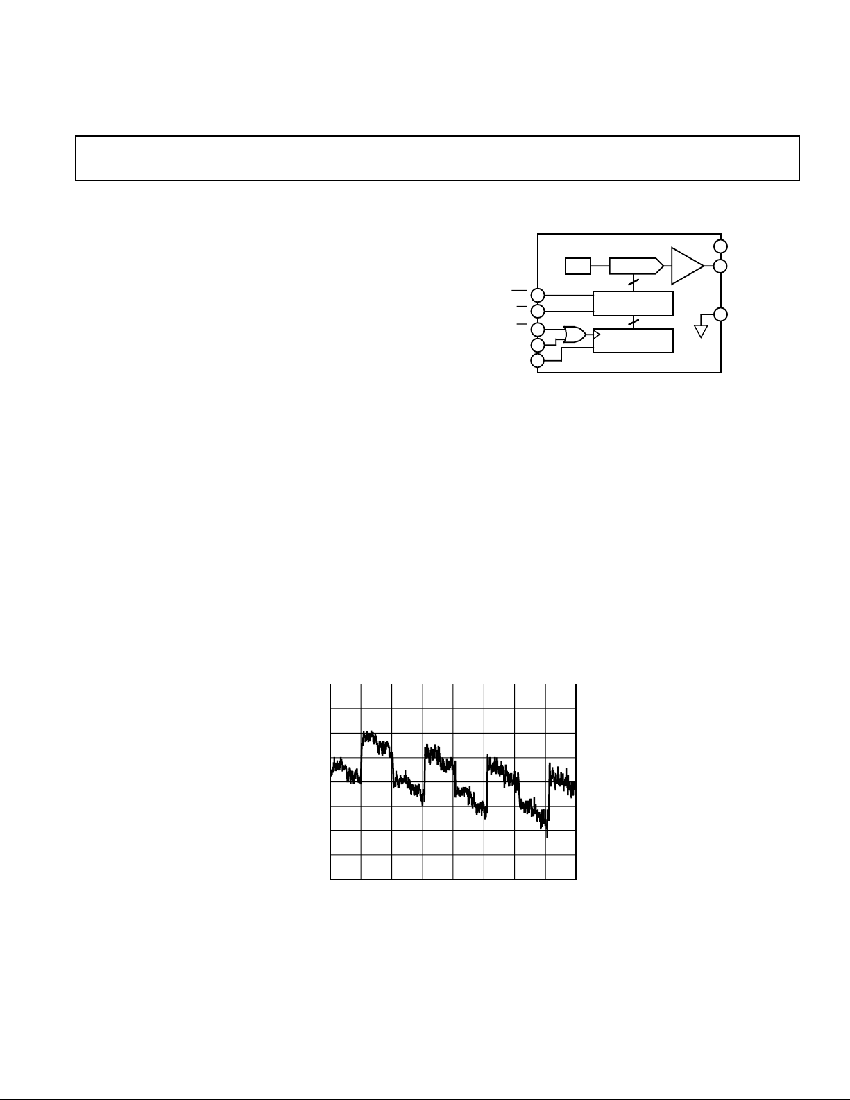
FUNCTIONAL BLOCK DIAGRAM
Serial interface is high speed, three-wire, DSP compatible with
data in (SDI), clock (CLK) and load strobe (LD). There is also
a chip-select pin for connecting multiple DACs.
A CLR input sets the output to zero scale at power on or upon
user demand.
The DAC8512 is specified over the extended industrial (–40°C
to +85°C) temperature range. DAC8512s are available in plastic DIPs and SO-8 surface mount packages.
1.0
0.75
0.5
0.25
0
–0.25
LINEARITY ERROR – LSB
–0.5
–0.75
–1.0
0
DIGITAL INPUT CODE – Decimal
307220481024
4096
Linearity Error vs. Digital Input Code
REV. A
Information furnished by Analog Devices is believed to be accurate and
reliable. However, no responsibility is assumed by Analog Devices for its
use, nor for any infringements of patents or other rights of third parties
which may result from its use. No license is granted by implication or
otherwise under any patent or patent rights of Analog Devices.
One Technology Way, P.O. Box 9106, Norwood, MA 02062-9106, U.S.A.
Tel: 617/329-4700 World Wide Web Site: http://www.analog.com
Fax: 617/326-8703 © Analog Devices, Inc., 1996

DAC8512–SPECIFICATIONS
(@ V
ELECTRICAL CHARACTERISTICS
Parameter Symbol Condition Min Typ Max Units
STATIC PERFORMANCE
Resolution N Note 2 12 Bits
Relative Accuracy INL E Grade –1 ±1/4 +1 LSB
Differential Nonlinearity DNL No Missing Codes –1 ±3/4 +1 LSB
Zero-Scale Error V
Full-Scale Voltage V
Full-Scale Tempco TCV
ANALOG OUTPUT
Output Current I
Load Regulation at Full Scale L
Capacitive Load C
LOGIC INPUTS
Logic Input Low Voltage V
Logic Input High Voltage V
Input Leakage Current I
Input Capacitance C
INTERFACE TIMING SPECIFICATIONS
Clock Width High t
Clock Width Low t
Load Pulse Width t
Data Setup t
Data Hold t
Clear Pulse Width t
Load Setup t
Load Hold t
Select t
Deselect t
AC CHARACTERISTICS
4
Voltage Output Settling Time t
DAC Glitch 15 nV s
Digital Feedthrough 15 nV s
ZSE
FS
FS
OUT
REG
L
IL
IH
IL
IL
1, 4
CH
CL
LDW
DS
DH
CLRW
LD1
LD2
CSS
CSH
S
= +5.0 V 6 5%, –408C ≤ TA ≤ +858C, unless otherwise noted)
DD
F Grade –2 ±3/4 +2 LSB
Data = 000
Data = FFF
H
3
H
E Grade 4.087 4.095 4.103 V
+1/2 +3 LSB
F Grade 4.079 4.095 4.111 V
Notes 3, 4 16 ppm/°C
Data = 800
R
= 402 Ω to ∞, Data = 800
L
No Oscillation
H
4
H
±5 ±7mA
1 3 LSB
500 pF
0.8 V
2.4 V
10 µA
10 pF
30 10 ns
30 10 ns
20 ns
15 10 ns
15 5 ns
30 20 ns
15 ns
10 ns
30 ns
20 ns
To ±1 LSB of Final Value
5
16 µs
SUPPLY CHARACTERISTICS
Positive Supply Current I
Power Dissipation P
DD
DISS
VIH = 2.4 V, VIL = 0.8 V, No Load 1.5 2.5 mA
V
= 5 V, VIL = 0 V, No Load 0.5 1 mA
DD
VIH = 2.4 V, VIL = 0.8 V, No Load 7.5 12.5 mW
V
= 5 V, VIL = 0 V, No Load 2.5 5 mW
DD
Power Supply Sensitivity PSS ∆VDD = ±5% 0.002 0.004 %/%
NOTES
1
All input control signals are specified with tr = tf = 5 ns (10% to 90% of +5 V) and timed from a voltage level of 1.6 V.
2
1 LSB = 1 mV for 0 V to +4.095 V output range.
3
Includes internal voltage reference error.
4
These parameters are guaranteed by design and not subject to production testing.
5
The settling time specification does not apply for negative going transitions within the last 6 LSBs of ground. Some devices exhibit double the typical settling time in
this 6 LSB region.
Specifications subject to change without notice.
–2–
REV. A

DAC8512
WAFER TEST LIMITS
(@ VDD = +5.0 V 6 5%, TA = +258C, applies to part number DAC8512GBC only, unless otherwise noted)
Parameter Symbol Condition Min Typ Max Units
STATIC PERFORMANCE
Relative Accuracy INL –2 ± 3/4 +2 LSB
Differential Nonlinearity DNL No Missing Codes –1 ±0.7 +1 LSB
Zero-Scale Error V
Full-Scale Voltage V
ZSE
FS
Data = 000
Data = FFF
H
H
4.085 4.095 4.105 V
+1/2 +3 LSB
LOGIC INPUTS
Logic Input Low Voltage V
Logic Input High Voltage V
Input Leakage Current I
IL
IH
IL
2.4 V
0.8 V
10 µA
SUPPLY CHARACTERISTICS
Positive Supply Current I
Power Dissipation P
DD
DISS
VIH = 2.4 V, VIL= 0.8 V, No Load 1.5 2.5 mA
V
= 5 V, VIL = 0 V, No Load 0.5 1 mA
DD
VIH = 2.4 V, VIL = 0.8 V, No Load 7.5 12.5 mW
V
= 5 V, VIL = 0 V, No Load 2.5 5 mW
DD
Power Supply Sensitivity PSS ∆VDD = ±5% 0.002 0.004 %/%
NOTE
Electrical tests are performed at wafer probe to the limits shown. Due to variations in assembly methods and normal yield loss, yield after packaging is not guaranteed
for standard product dice. Consult factory to negotiate specifications based on dice lot qualifications through sample lot assembly and testing.
ABSOLUTE MAXIMUM RATINGS*
VDD to GND . . . . . . . . . . . . . . . . . . . . . . . . . . . –0.3 V, +10 V
Logic Inputs to GND . . . . . . . . . . . . . . . –0.3 V, V
V
to GND . . . . . . . . . . . . . . . . . . . . . –0.3 V, VDD + 0.3 V
OUT
I
Short Circuit to GND . . . . . . . . . . . . . . . . . . . . . . 50 mA
OUT
Package Power Dissipation . . . . . . . . . . . . . .(T
Thermal Resistance θ
JA
+ 0.3 V
DD
max – T
J
)/θ
A
8-Pin Plastic DIP Package (P) . . . . . . . . . . . . . . . . 103°C/W
8-Lead SOIC Package (S) . . . . . . . . . . . . . . . . . . . 158°C/W
Maximum Junction Temperature (T
max) . . . . . . . . . +150°C
J
Operating Temperature Range . . . . . . . . . . . . .–40°C to +85°C
Storage Temperature Range . . . . . . . . . . . . .–65°C to +150°C
Lead Temperature (Soldering, 10 secs) . . . . . . . . . . . . +300°C
*Stresses above those listed under “Absolute Maximum Ratings” may cause
permanent damage to the device. This is a stress rating only and functional
JA
operation of the device at these or any other conditions above those indicated in the
operational sections of this specification is not implied. Exposure to absolute
maximum rating conditions for extended periods may affect device reliability .
CAUTION
ESD (electrostatic discharge) sensitive device. Electrostatic charges as high as 4000 V readily
accumulate on the human body and test equipment and can discharge without detection.
Although the DAC8512 features proprietary ESD protection circuitry, permanent damage may
occur on devices subjected to high energy electrostatic discharges. Therefore, proper ESD
precautions are recommended to avoid performance degradation or loss of functionality.
ORDERING GUIDE
INL Temperature Package Package
Model (LSB) Range Description Option
DAC8512EP ±1 –40°C to +85°C 8-Pin P-DIP N-8
DAC8512FP ±2 –40°C to +85°C 8-Pin P-DIP N-8
DAC8512FS ±2 –40°C to +85° C 8-Lead SOIC SO-8
DAC8512GBC ±2 +25°C Dice
WARNING!
ESD SENSITIVE DEVICE
REV. A
–3–

DAC8512
SDI
CLK
CS
LD
SDI
CLK
LD
CLR
FS
V
OUT
ZS
D11 D10 D9 D8 D7 D6 D5 D3D4 D1D2 D0
t
css
t
ld1
t
t
ds
t
cl
dh
t
ch
t
ldw
t
s
±1 LSB
ERROR BAND
t
csh
t
ld2
t
clrw
t
S
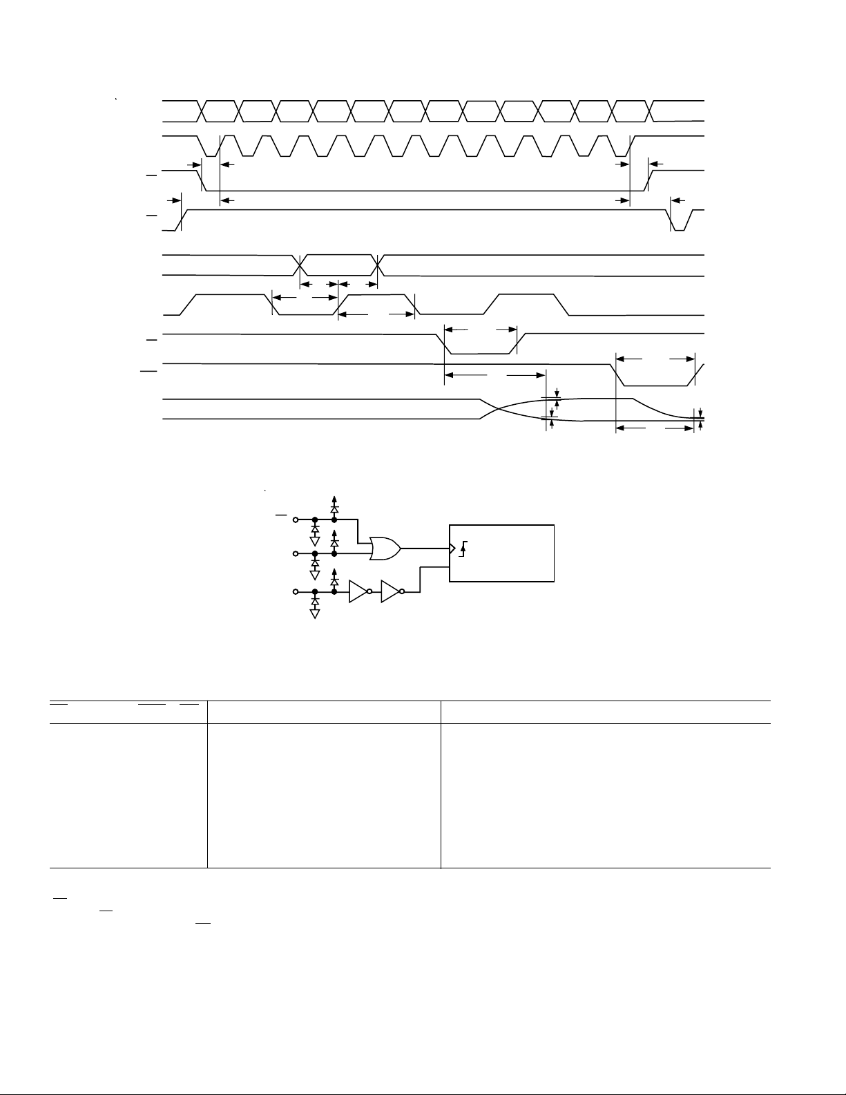
Figure 1. Timing Diagram
CS
ESD PROTECTION DIODES TO VDD AND GND
CLK
DATA
SDI
SHIFT
REGISTER
Figure 2. Equivalent Clock Input Logic
Table I. Control-Logic Truth Table
CS2CLK2CLR LD Serial Shift Register Function DAC Register Function
H X H H No Effect Latched
L L H H No Effect Latched
L H H H No Effect Latched
L ↑+ H H Shift-Register-Data Advanced One Bit Latched
↑+ L H H Shift-Register-Data Advanced One Bit Latched
HX H↓– No Effect Updated with Current Shift Register Contents
H X H L No Effect Transparent
H X L X No Effect Loaded with All Zeros
HX ↑+ H No Effect Latched All Zeros
NOTES
l
↑+ positive logic transition; ↓– negative logic transition; X = Don’t Care.
2
CS and CLK are interchangeable.
3
Returning CS HIGH avoids an additional “false clock” of serial data input.
4
Do not clock in serial data while LD is LOW.
–4–
REV. A

DAC8512
R1
R2
V
OUT
RAIL-TO-RAIL
OUTPUT
AMPLIFIER
R
BANDGAP
REFERENCE
2R
R
2R
2R
2R
SPDT
N-CH FET
SWITCHES
2R
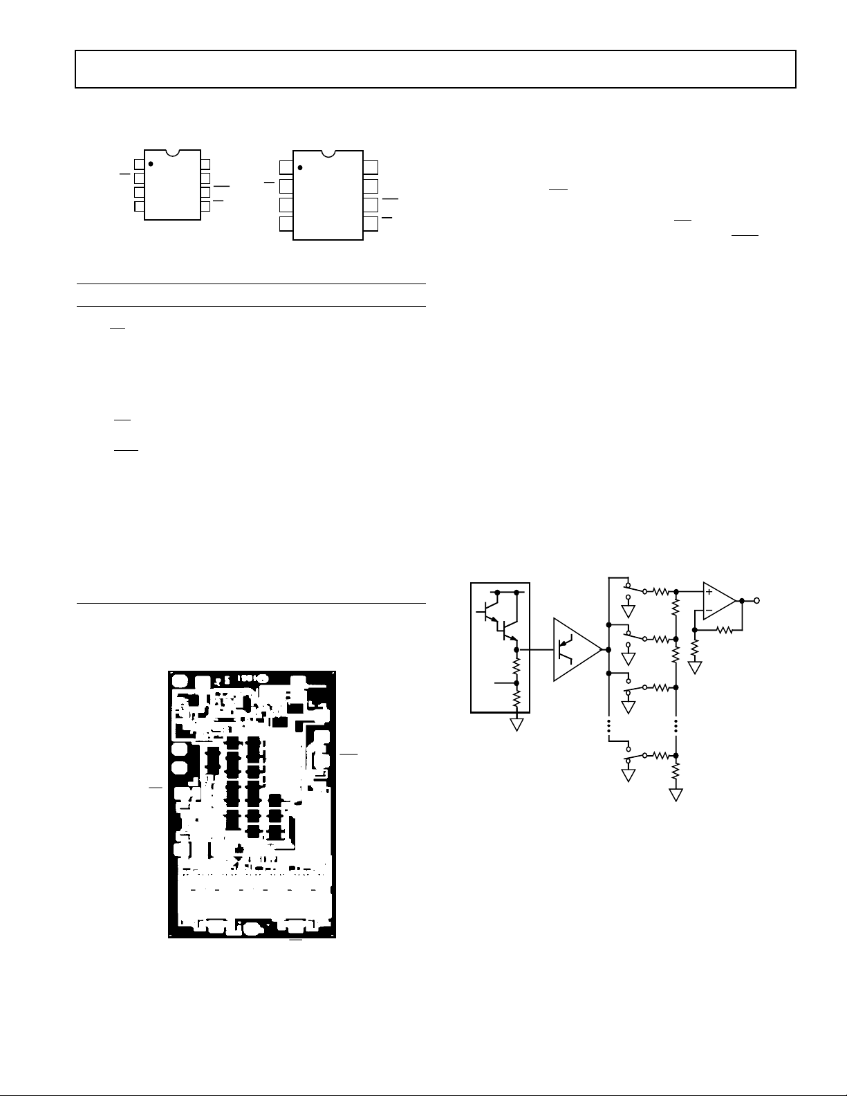
AV = 4.095/2.5
= 1.638V/V
VOLTAGE SWITCHED 12-BIT
R-2R D/A CONVERTER
BUFFER
2.5V
PIN CONFIGURATIONS
SO-8 P-DIP-8 & Cerdip-8
V
CS
CLK
SDI
DD
1
DAC8512
2
TOP VIEW
3
(Not to Scale)
4
V
OUT
8
GND
7
CLR
6
LD
5
V
CS
CLK
SDI
DD
1
2
3
(Not to Scale)
4
DAC8512
TOP VIEW
8
V
OUT
GND
7
CLR
6
LD
5
PIN DESCRIPTIONS
Pin Name Description
1VDDPositive Supply. Nominal value +5 V, ± 5%.
CS Chip Select. Active low input.
2
3 CLK Clock input for the internal serial input shift register.
4 SDI Serial Data Input. Data on this pin is clocked into the
internal serial register on positive clock edges of the
CLK pin. The Most Significant Bit (MSB) is loaded
first.
LD Active low input which writes the serial register data
5
into the DAC register. Asynchronous input.
CLR Active low digital input that clears the DAC register to
6
zero, setting the DAC to minimum scale. Asynchronous
input.
7 GND Analog ground for the DAC. This also serves as the
digital logic ground reference voltage.
8V
Voltage output from the DAC. Fixed output voltage
OUT
range of 0 V to 4.095 V with 1 mV/LSB. An internal
temperature stabilized reference maintains a fixed
full-scale voltage independent of time, temperature and
power supply variations.
OPERATION
The DAC8512 is a complete ready to use 12-bit digital-to-analog
converter. It contains a voltage-switched, 12-bit, laser-trimmed
DAC, a curvature-corrected bandgap reference, a rail-to-rail
output op amp, a DAC register, and a serial data input register.
The serial data interface consists of a CLK, serial data in (SDI),
and a load strobe (
LD). This basic 3-wire interface offers maximum flexibility for interface to the widest variety of serial data
input loading requirements. In addition a
for multiple packaging loading and a power on reset
CS select is provided
CLR pin to
simplify start or periodic resets.
D/A CONVERTER SECTION
The DAC is a 12-bit voltage mode device with an output that
swings from GND potential to the 2.5 volt internal bandgap
voltage. It uses a laser trimmed R-2R ladder which is switched
by N channel MOSFETs. The output voltage of the DAC has a
constant resistance independent of digital input code. The DAC
output is internally connected to the rail-to-rail output op amp.
AMPLIFIER SECTION
The DAC’s output is buffered by a low power consumption precision amplifier. This amplifier contains a differential PNP pair
input stage which provides low offset voltage and low noise, as
well as the ability to amplify the zero-scale DAC output voltages. The rail-to-rail amplifier is configured in a gain of 1.6384
(= 4.095 V/2.5 V) in order to set the 4.095 volt full-scale output
(1 mV/LSB). See Figure 3 for an equivalent circuit schematic of
the analog section.
DICE CHARACTERISTICS
2
CS
3
CLK
SUBSTRATE IS COMMON WITH VDD.
NUMBER OF TRANSISTORS: 642
DIE SIZE: 0.055 inch × 0.106 inch; 5830 sq mils
V
DD
1
4
SDI LD
V
OUT
8
GND
7
GND
7
6
CLR
Figure 3. Equivalent DAC8512 Schematic of Analog
Portion
The op amp has a 16 µs typical settling time to 0.01%. There
are slight differences in settling time for negative slowing signals
5
vs. positive. See the oscilloscope photos in the typical performances section of this data sheet.
REV. A
–5–

DAC8512
OUTPUT SECTION
The rail-to-rail output stage of this amplifier has been designed
to provide precision performance while operating near either
power supply.
V
DD
P-CH
V
N-CH
OUT
AGND
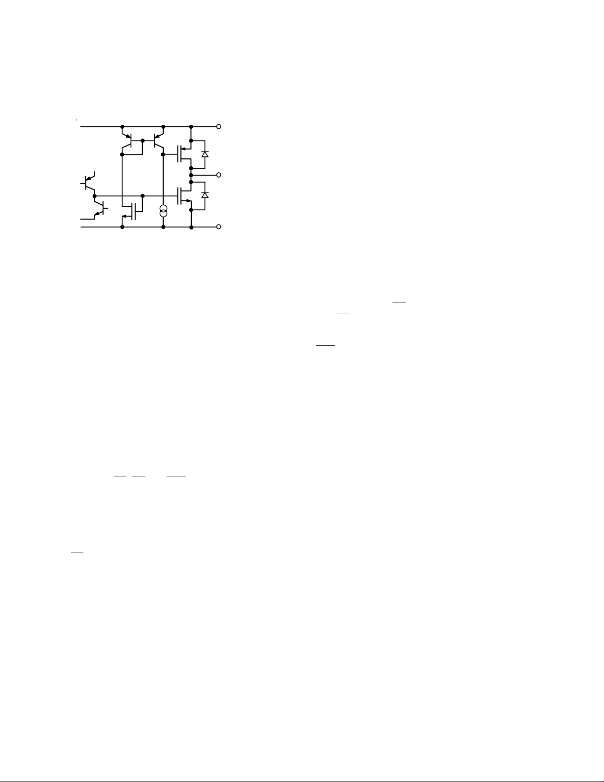
Figure 4. Equivalent Analog Output Circuit
Figure 4 shows an equivalent output schematic of the rail-to-rail
amplifier with its N channel pull down FETs that will pull an
output load directly to GND. The output sourcing current is
provided by a P channel pull up device that can supply GND
terminated loads, especially at the low supply tolerance values of
4.75 volts. Figures 5 and 6 provide information on output swing
performance near ground and full-scale as a function of load. In
addition to resistive load driving capability the amplifier has also
been carefully designed and characterized for up to 500 pF capacitive load driving capability.
POWER SUPPLY
The very low power consumption of the DAC8512 is a direct
result of a circuit design optimizing use of the CBCMOS process. By using the low power characteristics of the CMOS for
the logic, and the low noise, tight matching of the complementary bipolar transistors good analog accuracy is achieved.
For power consumption sensitive applications it is important to
note that the internal power consumption of the DAC8512 is
strongly dependent on the actual logic input voltage levels
present on the SDI,
CS, LD, and CLR pins. Since these inputs
are standard CMOS logic structures they contribute static
power dissipation dependent on the actual driving logic V
V
voltage levels. The graph in Figure 9 shows the effect on to-
OL
OH
and
tal DAC8512 supply current as a function of the actual value of
input logic voltage. Consequently use of CMOS logic vs. TTL
minimizes power dissipation in the static state. A V
the SDI,
CS and CLR pins provides the lowest standby power
= 0 V on
IL
dissipation of 2.5 mW (500 µA × 5 V).
As with any analog system, it is recommended that the DAC8512
power supply be bypassed on the same PC card that contains the
chip. Figure 10 shows the power supply rejection versus frequency performance. This should be taken into account when using
higher frequency switched mode power supplies with ripple frequencies of 100 kHz and higher.
One advantage of the rail-to-rail output amplifier used in the
DAC8512 is the wide range of usable supply voltage. The part
is fully specified and tested over temperature for operation from
+4.75 V to +5.25 V. If reduced linearity and source current capability near full scale can be tolerated, operation of the DAC8512
is possible down to +4.3 volts. The minimum operating supply
voltage versus load current plot, in Figure 11, provides information for operation below V
TIMING AND CONTROL
= +4.75 V.
DD
The DAC8512 has a separate serial input register from the
12-bit DAC register that allows preloading of a new data value
into the serial register without disturbing the present DAC output voltage. After the new value is fully loaded in the serial input register it can be asynchronously transferred to the DAC
register by strobing the
sensitive
LD strobe that should be returned high before any
LD pin. The DAC register uses a level
new data is loaded into the serial input register. At any time the
contents of the DAC register can be reset to zero by strobing
the
CLR pin which causes the DAC output voltage to go to
zero volts. All of the timing requirements are detailed in Figure
1 along with the Table I Control-Logic Truth Table.
–6–
REV. A
