

Quad 8-Bit Voltage Out CMOS DAC
a
FEATURES
No Adjustments Required, Total Error 61 LSB Max
Over Temperature
Four Voltage-Output DACs on a Single Chip
Internal 10 V Bandgap Reference
Operates from Single 115 V Supply
Fast 50 ns Data Load Time, All Temperatures
Pin-for-Pin Replacement for PM-7226 and AD7226,
Eliminates External Reference
APPLICATIONS
Process Controls
Multichannel Microprocessor Controlled:
System Calibration
Op Amp Offset and Gain Adjust
Level and Threshold Setting
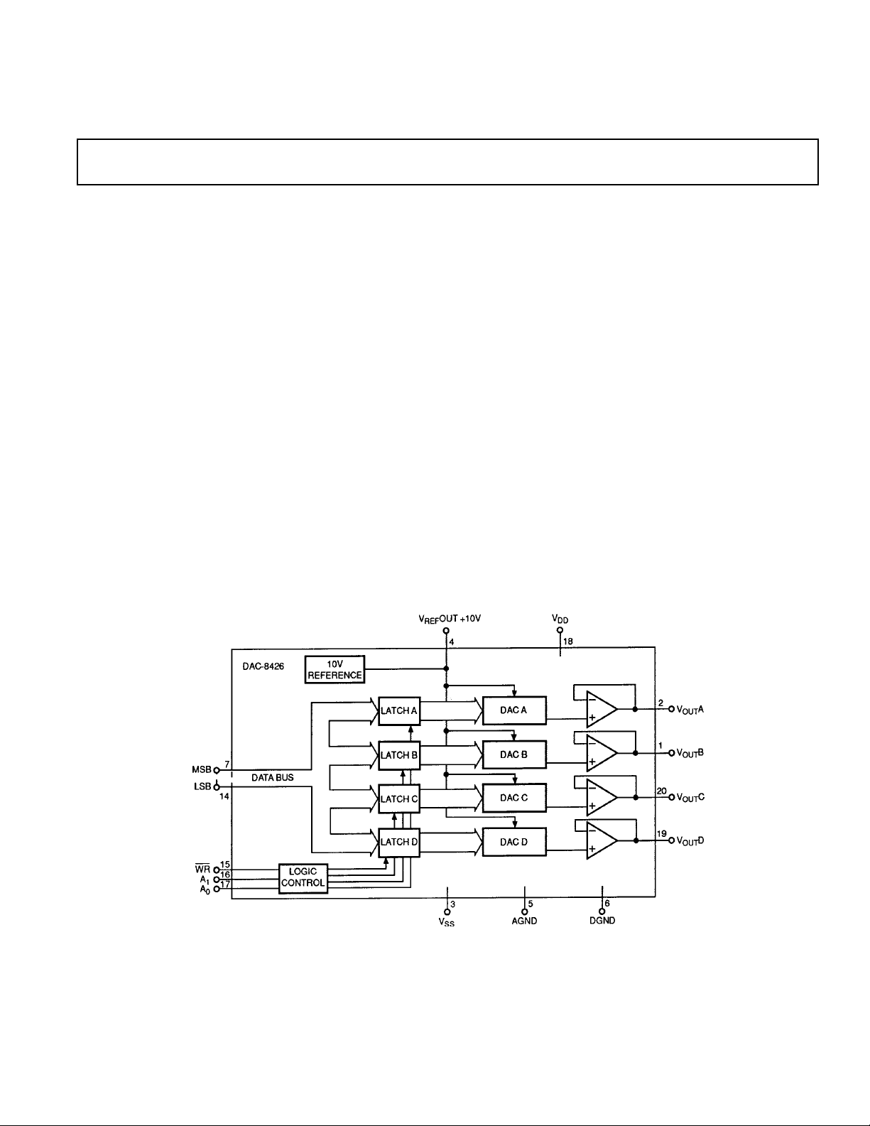
GENERAL DESCRIPTION
The DAC8426 is a complete quad voltage output D/A converter
with internal reference. This product fits directly into any existing 7226 socket where the user currently has a 10 V external
reference. The external reference is no longer necessary. The
internal reference of the DAC8426 is laser-trimmed to ±0.4%
Complete with Internal 10 V Reference
DAC8426
offering a 25 ppm/°C temperature coefficient and 5 mA of external load driving capability.
The DAC8426 contains four 8-bit voltage-output CMOS D/A
converters on a single chip. A 10 V output bandgap reference
sets the output full-scale voltage. The circuit also includes four
input latches and interface control logic.
One of the four latches, selected by the address inputs, is loaded
from the 8-bit data bus input when the write strobe is active
low. All digital inputs are TTL/CMOS (5 V) compatible. The
on-board amplifiers can drive up to 10 mA from either a single
or dual supply. The on-board reference that is always connected
to the internal DACs has 5 mA available to drive external devices.
Its compact size, low power, and economical cost-per-channel,
make the DAC8426 attractive for applications requiring multiple D/A converters without sacrificing circuit-board space. System reliability is also increased due to reduced parts count.
PMI’s advanced oxide-based, silicon-gate, CMOS process allows the DAC8426’s analog and digital circuitry to be manufactured on the same chip. This, coupled with PMI’s highly stable
thin-film R-2R resistor ladder, aids in matching and temperature tracking between DACs.
FUNCTIONAL BLOCK DIAGRAM
REV. C
Information furnished by Analog Devices is believed to be accurate and
reliable. However, no responsibility is assumed by Analog Devices for its
use, nor for any infringements of patents or other rights of third parties
which may result from its use. No license is granted by implication or
otherwise under any patent or patent rights of Analog Devices.
One Technology Way, P.O. Box 9106, Norwood, MA 02062-9106, U.S.A.
Tel: 617/329-4700 Fax: 617/326-8703

DAC8426–SPECIFICA TIONS
(VDD = +15 V 6 10%, AGND = DGND = 0 V, VSS = 0 V, TA = –558C to +1258C
applies for DAC8426AR/BR, TA = –408C to +858C applies for DAC8426ER/EP/FR/FP/FS, unless otherwise noted.)
Parameter Symbol Conditions Min Typ Max Units
STATIC PERFORMANCE
Resolution N 8 Bits
Total Unadjusted Error
Relative Accuracy INL A, E ±1/2 LSB
Differential Nonlinearity
Full-Scale Temperature Coefficient TCG
Zero Scale Error V
Zero Scale Error
Temperature Coefficient TCV
REFERENCE OUTPUT
Output Voltage V
Temperature Coefficient TCV
Load Regulation LD
Line Regulation LN
Output Noise
3
Output Current I
DIGITAL INPUTS
Logic Input “0” V
Logic Input “1” V
Input Current I
Input Capacitance
POWER SUPPLIES
Positive Supply Current
Negative Supply Current
Power Dissipation
Power Supply Sensitivity P
1
TUE Includes Reference A, E ±1 LSB
B, F ±2 LSB
2
DNL ±1 LSB
FS
ZSE
ZS
OUT No Load A, E 9.96 10.04 V
REF
Includes Reference 25 ppm/°C
Dual Supply VSS = –5 V 10 µV/°C
B, F ±1 LSB
20 mV
B, F 9.92 10.08 V
OUT 20 ppm/°C
REF
REG
REG
∆IL = 5 mA 0.02 0.1 %/mA
∆VDD ±10% 0.008 0.04 %/V
en rms f = 0.1 Hz to 10 Hz 3 10 µV p-p
OUT ∆V
REF
INL
INH
3
4
4
5
C
I
I
P
IN
IN
DD
SS
DISS
SS
OUT < 40 mV 5 7 mA
REF
0.8 V
2.4 V
VIN = 0 V or V
DD
0.1 10 µA
48pF
614mA
Dual Supply VSS = –5 V 4 10 mA
90 210 mW
∆VDD = ±5% 0.0002 0.01 %/%
ELECTRICAL CHARACTERISTICS
VDD = +15 V 6 10%, AGND = DGND = 0 V, VSS = 0 V, TA = –558C to +1258C applies for
DAC8426AR/BR, TA = –408C to +858C applies for DAC8426ER/EP/FR/FP/FS, unless otherwise noted.
Parameter Symbol Conditions Min Typ6Max Units
DAC OUTPUT
Output Current (Source)
Output Current (Sink)
Minimum Load Resistance R
DYNAMIC PERFORMANCE
V
Slew Rate SR 4 V/µs
OUT
V
Settling Time t
OUT
(Positive or Negative)
Digital Crosstalk Q 10 nVs
SWITCHING CHARACTERISTICS
Address To Write Setup Time t
Address To Write Hold Time t
Data Valid To Write Setup Time t
Data Valid To Write Hold Time t
Write Pulse Width t
NOTES
1
Includes Full-Scale Error, Relative Accuracy, and Zero Code Error. Note ± 1 LSB = ±0.39% error.
2
All devices guaranteed monotonic over the full operating temperature range.
3
Guaranteed and not subject to production test.
4
Digital inputs VIN = V
5
P
calculated by IDD × VDD.
DISS
6
Typicals represent measured characteristics at TA = +25°C.
Specifications subject to change without notice.
INL
or V
3
3
3
; V
OUT
and V
INH
I
OUT
I
OUT
S
3
AS
AH
DS
DH
WR
OUT unloaded.
REF
SOURCE Digital In = All Ones 10 mA
SINK Digital In = All Zeroes VSS = –5 V 350 450 µA
L(MIN)
Digital In = All Ones 2 kΩ
To ±1/2 LSB, RL = 2 kΩ 3 µs
0ns
0ns
70 ns
10 ns
50 ns
–2–
REV. C
DAC8426
ABSOLUTE MAXIMUM RATINGS
VDD to AGND or DGND . . . . . . . . . . . . . . . . .–0.3 V, +17 V
V
to AGND or DGND . . . . . . . . . . . . . . . . . . . . .–7 V, V
SS
DD
VDD to VSS . . . . . . . . . . . . . . . . . . . . . . . . . . . .–0.3 V, +24 V
AGND to DGND . . . . . . . . . . . . . . . . . . . . . . . .–0.3 V, +5 V
Digital Input Voltage to DGND . . . . . . . . . . . . . –0.3 V, V
V
OUT to AGND1 . . . . . . . . . . . . . . . . . . . . . –0.3 V, V
REF
V
to AGND1 . . . . . . . . . . . . . . . . . . . . . . . . . . . . VSS, V
OUT
DD
DD
DD
Operating Temperature
Military AR/BR . . . . . . . . . . . . . . . . . . . . –55°C to +125°C
Extended Industrial ER/EP/FR/FP/FS . . . . –40°C to +85°C
Maximum Junction Temperature . . . . . . . . . . . . . . . . +150°C
Storage Temperature . . . . . . . . . . . . . . . . . . –65°C to +150°C
Lead Temperature (Soldering, 60 sec) . . . . . . . . . . . . +300°C
THERMAL RESISTANCE
Package Type u
2
JA
u
JC
Units
20-Pin Cerdip (R) 70 7 °C/W
20-Pin Plastic DIP (P) 61 24 °C/W
20-Pin SOL(S) 80 22 °C/W
NOTES
1
Outputs may be shorted to any terminal provided the package power dissipation
is not exceeded. Typical output short-circuit current to AGND is 50 mA.
2
θJA is specified for worst case mounting conditions, i.e., θJA is specified for de-
vice in socket for cerdip and P-DIP packages; θJA is specified for device soldered to printed circuit board for SOL package.
ORDERING GUIDE
CAUTION
1. Do not apply voltages higher than VDD or less than VSS potential on any terminal.
2. The digital control inputs are zener-protected; however,
permanent damage may occur on unprotected units from
high-energy electrostatic fields. Keep units in conductive
foam at all times until ready to use.
3. Do not insert this device into powered sockets. Remove
power before insertion or removal.
4. Stresses above those listed under “Absolute Maximum Ratings” may cause permanent damage to device.
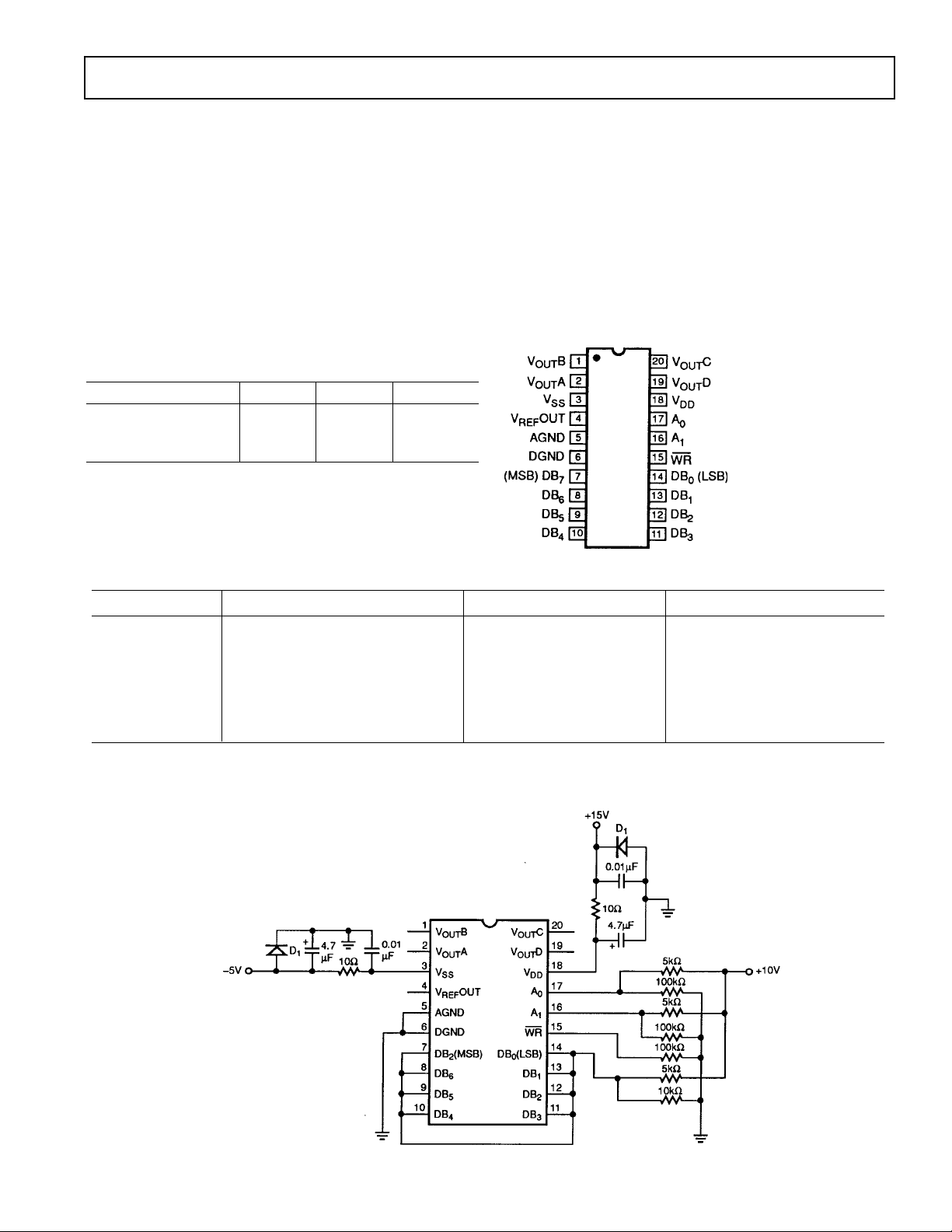
PIN CONNECTIONS
20-Pin Cerdip
(R Suffix)
20-Pin Epoxy DIP
(P Suffix)
20-Pin SOL
(S Suffix)
1
Model Total Unadjusted Error Temperature Range Package Description
DAC8426AR
2
±1 LSB –55°C to +125°C 20-Pin Cerdip (Q-20)
DAC8426ER ±1 LSB –40°C to +85°C 20-Pin Cerdip (Q-20)
DAC8426EP ±1 LSB –40°C to +85°C 20-Pin Plastic DIP (N-20)
DAC8426BR
2
±2 LSB –55°C to +125°C 20-Pin Cerdip (Q-20)
DAC8426FR ±2 LSB –40°C to +85°C 20-Pin Cerdip (Q-20)
DAC8426FP ±2 LSB –40°C to +85°C 20-Pin Plastic DIP (N-20)
DAC8426FS
NOTES
1
Burn-in is available on commercial and industrial temperature range parts in cerdip, plastic DIP, and TO-can packages.
2
For devices processed in total compliance to MIL-STD-883, add /883 after part number. Consult factory for 883 data sheet.
3
For availability and burn-in information on SO and PLCC packages, contact your local sales office.
3
±2 LSB –40°C to +85°C 20-Lead SOL (R-20)
REV. C
Burn-In Circuit
–3–
DAC8426
WARNING!
ESD SENSITIVE DEVICE
DICE CHARACTERISTICS
1. V
OUT B
2. V
OUT A
3. V
SS
4. V
OUT 14. DB0 (LSB)
REF
11. DB
12. DB
13. DB
3
2
1
5. AGND 15. WR
6. DGND 16. A
7. DB7 (MSB) 17. A
8. DB
6
9. DB
5
10. DB
4
18. V
19. V
20. V
1
0
DD
OUT D
OUT C
DIE SIZE 0.129 × 0.152 inch, 19,608 sq. mils
×
3.86 mm, 12.65 sq. mm)
(3.28
WAFER TEST LIMITS
at VDD = +15 V 6 5%; VSS = AGND = DGND = 0 V; unless otherwise specified. TA = +258C. All specifications
apply for DACs A, B, C, and D.
DAC8426GBC
Parameter Symbol Conditions Limits Units
Total Unadjusted Error TUE ±2 LSB max
Relative Accuracy INL ±1 LSB max
Differential Nonlinearity DNL ± 1 LSB max
Full-Scale Error G
Zero Code Error V
DAC Output Current I
Reference Output Voltage V
Load Regulation LD
Line Regulation LN
Reference Output Current I
Logic Inputs High V
Logic Inputs Low V
Logic Input Current I
Positive Supply Current I
Negative Supply Current I
NOTE
Electrical tests are performed at wafer probe to the limits shown. Due to variations in assembly methods and normal yield loss, yield after packaging is not guaranteed
for standard product dice. Consult factory to negotiate specifications based on dice lot qualifications through sample lot assembly and testing.
FSE
ZSE
SOURCE Digital In = All Ones 10 mA min
OUT
OUT No Load 10.04 V max
REF
REG
REG
OUT ∆V
REF
INH
INL
IN
DD
SS
∆IL = 5 mA 0.1 %/mA max
∆VDD = ±10 V 0.04 %/V max
OUT < 40 mV 5 mA min
REF
V
= 0 V or V
IN
VIN = V
VIN = V
INL
INL
or V
or V
DD
INH
INH’ VSS
= –5 V 10 mA max
±1 LSB max
±20 mV max
2.4 V min
0.8 V max
±1 µA max
14 mA max
CAUTION
ESD (electrostatic discharge) sensitive device. Electrostatic charges as high as 4000 V readily
accumulate on the human body and test equipment and can discharge without detection.
Although the DAC8426 features proprietary ESD protection circuitry, permanent damage may
occur on devices subjected to high energy electrostatic discharges. Therefore, proper ESD
precautions are recommended to avoid performance degradation or loss of functionality.
–4–
REV. C

Typical Performance Characteristics–
DAC8426
Channel-to-Channel Matching (DACs
A, B, C, D, Superimposed)
Long Term Drift Accelerated by
Burn-In
Relative Accuracy vs. Code
= –55°C, +25°C, +125°C
at T
A
(All Superimposed)
V
Noise Density vs. Frequency
OUT
Zero Code Error vs. Temperature
Broadband Noise (DC to 200 kHz)
PSRR
=
V
DD
PSRR
VDD =
(+)
=
–20
LOG
+15
V 61 VP, VSS = 0 V
(–)
=
–20
LOG
+15
V, VSS =
V
OUT
D
V
OUT
D
–4 V 61
(0)
V
DD
(0)
V
SS
V
P
,
,
Power Supply Current vs.
Temperature
REV. C
PSRR vs. Frequency
–5–

DAC8426–
V
OUT Error from 10.000 V
REF
vs. Temperature
Typical Performance Characteristics
Output Impedance (V
vs. Frequency
REF
OUT)
V
OUT Load Regulation
REF
vs. Temperature
V
OUT Line Regulation vs. Temperature
REF
V
OUT Start Up
REF
–6–
REV. C

DAC8426
PARAMETER DEFINITIONS
TOTAL UNADJUSTED ERROR (TUE)
This specification includes the Full-Scale-Error, Relative Accuracy Zero-Code-Error and the internal reference voltage. The
ideal Full-Scale output voltage is 10 V minus 1 LSB which
equals 9.961 volts. Each LSB equals 10 V × (1/256) = 0.039 volts.
DIGITAL CROSSTALK
Digital crosstalk is the signal coupled to the output of a DAC
due to a changing digital input from adjacent DACs being updated. It is specified in nano-Volt-seconds (nVs).
CIRCUIT DESCRIPTION
The DAC8426 is a complete quad 8-bit D/A converter. It contains an internal bandgap reference, four voltage switched R-2R
ladder DACs, four DAC latches, four output buffer amplifiers,
and an address decoder. All four DACs share the internal ten
volt reference and analog ground(AGND). Figure 1 provides an
equivalent DAC plus buffer schematic.
Table I. DAC Control Logic Truth Table
Logic Control DAC8426
WR A
1
A
0
Operation
H X X No Operation
Device Not Selected
L L L DAC A Transparent
g L L DAC A Latched
L L H DAC B Transparent
g L H DAC B Latched
L H L DAC C Transparent
g H L DAC C Latched
L H H DAC D Transparent
g H H DAC D Latched
L = Low State, H = High State, X = Don’t Care
Figure 1. Simplified Circuit Configuration for One DAC.
(Switches Are Shown for All “1s” on the Digital Inputs.)
The eleven digital inputs are compatible with both TTL and 5 V
(or higher) CMOS logic. Table I shows the DAC control logic
truth table for
WR, A1, and A0 operation. When WR is active
low the input latch of the selected DAC is transparent, and the
DAC’s output responds to the data present on the eight digital
data inputs (DBx). The data (DBx) is latched into the addressed DAC’s latch on the positive edge of the
WR control signal. The important timing requirements are shown in the Write
Cycle Timing Diagram, Figure 2.
INTERNAL 10 VOLT REFERENCE
The internal 10 V bandgap reference of the DAC8426 is trimmed to the output voltage and temperature drift specifications.
This internal reference is connected to the reference inputs of
the four internal 8-bit D/A converters. The output terminal of
the internal 10 V reference is available on pin 4. The 10 V output of the reference is produced with respect to the AGND pin.
This reference output can be used to supply as much as 5 mA of
additional current to external devices. Care has been taken in
Figure 2. Write Cycle Timing Diagram
the design of the internal DAC switching to minimize transients
on the reference voltage terminal (V
OUT). Other devices
REF
connected to this reference terminal should have well behaved
input loading characteristics. D/A converters such as the PMI
PM7226A have been designed to minimize reference input transient currents and can be directly connected to the DAC8426
10 V reference. Devices exhibiting large current transients due
to internal switching should be buffered with an op amp to
maintain good overall system noise performance. A 10 µF refer-
ence output bypass capacitor is required.
BUFFER AMPLIFIER SECTION
The four internal unity-gain voltage buffers provide low output
impedance capable of sourcing 5 mA or sinking 350 µA. Typical
output slew rates of ±4 V/µs are achieved with 10 V full-scale out-
put changes and R
= 2 kΩ. Figure 3 photographs show large sig-
L
nal and settling time response. Capacitive loads to 3300 pF
maximum, and resistive loads to 2 kΩ minimum can be applied.
REV. C
–7–

DAC8426
a) Large Signal
b) Settling Time Response (Negative Transition)
c) Settling Time Response (Positive Transition)
Figure 3. Dynamic Response
The outputs can withstand an indefinite short-circuit to AGND
to typically 50 mA. The output may also be shorted to any voltage between V
and VSS; however, care must be taken to not
DD
exceed the device maximum power dissipation.
The amplifier’s emitter follower output stage consists of an in-
trinsic NPN bipolar transistor with a 400 µA NMOS pull-down
current-source load connected to V
. This circuit configuration
SS
shown in Figure 4 enables the output amplifier to develop output voltages very close to AGND. Only the negative supply of the
Test Conditions, All Photos:
V
= +15 V
DD
OUT = 10 mF
C
REF
= 2 kV
R
L
Digital Input Sequence 0, 255, 0
four output buffer amplifiers are connected to V
the DAC8426 from dual supplies (V
= +15 V and VSS = –5 V)
DD
. Operating
SS
improves negative going output settling time near zero volts.
When operating single supply (V
= +15 V and VSS = 0 V) the
DD
output sink current decreases as the output approaches zero
voltage. Within 200 mV of AGND (single-supply operation) the
internal sinking capability appears resistive at a value of approximately 1200 Ω. The buffer amplifier output current and voltage
characteristics are plotted in Figure 5.
–8–
REV. C

DAC8426
APPLICATIONS SETUP
UNIPOLAR OUTPUT OPERATION
The output voltage appearing at any output V
internal 10 V reference multiplied by the decimal value of the
latched digital input divided by 2
V
(D) = D/256 × 10 V
OUT
where D = 0
to 255
10
10
8
(= 256). In equation form:
is equal to the
OUT
Figure 4. Amplifier Output Stage
Note that the maximum possible output is 1 LSB less than the
internal 10 V reference, that is, 255/256 × 10 V = 9.961 V.
Table II lists output voltages for a given digital input. The total
unadjusted error (TUE) specification of the product grade used
determines the output tolerances of the values listed in Table II.
For example, a ±2 LSB grade DAC8426FP loaded with decimal
128
(half-scale) would have a guaranteed output voltage oc-
10
curring in the range of 5 V ±2 LSB, which is 5 V ±(2 × 10 V/256)
= 5 V ±0.078 V. Therefore V
is guaranteed to occur in the
OUT
following range:
4.922 V ≤ V
(128) ≤ 5.078 V
OUT
One additional characteristic guaranteed is a DNL of ±1 LSB
on all grades. The DAC8426 is therefore guaranteed to be monotonic. In the situation where a continuously positive 1 LSB
digital increment is applied, the output voltage will always increase in value, never decrease. This is very important is servo
applications and other closed-loop feedback systems. Finally, in
the typical characteristic curves, long term output voltage drift
(stability) is provided.
BIPOLAR OUTPUT OPERATION
An external op amp plus two resistors can easily convert any
DAC output to bipolar output voltage swings. Figure 6 shows all
four DACs output operating in bipolar mode. This is the general
expression describing the bipolar output transfer equation:
V
(D) = [(1 +R2/R1) × D/256 × 10 V] –R2/R1 × 10 V,
OUT
where D = 0
If R1 = R2, then V
Table III lists various output voltages with R
to 255
10
10
becomes:
OUT
(D) = (D/128–1) × 10 V
V
OUT
= R2 versus digital
1
input code. This coding is considered offset binary. Note that
the LSB step size is now 20 V/256 = 0.078 V, twice as large as
the unipolar output case previously discussed. In order to minimize
gain and offset errors, choose R
and R2 to match and track
1
within 0.1% over the selected operating temperature range
of interest.
Table II. Unipolar Output Voltage as a Function of
Digital Input Code
Digital Input Analog Output
Code Voltage (= D/256 × 10 V)
255 9.961 V Full-Scale (FS)
254 9.922 V FS-1 LSB
129 5.039 V
128 5.000 V Half-Scale
127 4.961 V
1 0.039 V 1 LSB
0 0.000 V Zero-Scale
Figure 5. DAC Output Current Sink
For the top grade DAC8426EP ±1 LSB total unadjusted error
(TUE), the guaranteed range is 4.961 V ≤ V
(12810) ≤ 5.039 V.
OUT
These tolerances provide the worst case analysis including temperature changes.
REV. C
–9–
OFFSETTING AGND
Since the DAC ladder and bandgap reference are terminated at
AGND, it is possible to offset AGND positive with respect to
DGND. The 10 V output span remains if a positive offset is applied to AGND. The offset voltage source connected to AGND
must be capable of sinking 14 mA. AGND cannot be taken
negative with respect to DGND; this would forward bias an internal diode. Allowance must be made at V
of headroom above V
OUT. This connection setup is useful
REF
to maintain 3.5 V
DD
in single supply applications where virtual ground needs to be
slightly positive with respect to ground. In this application connect V
to DGND to take advantage of the extra buffer output
SS
current sinking capability when the DAC output is programmed
to all zeros code, see Figure 7.

DAC8426
Table III. Bipolar Output Voltage as a Function of Digital
Input Code
Digital Input Analog Output
Code Voltage (= D/256 × 10 V)
255 9.922 V Full-Scale (FS)
254 9.844 V FS-1 LSB
129 0.078 V
128 0.000 V Zero-Scale
127 –0.078 V
1 –9.922 V
0 –10.000 V Neg Full-Scale
Figure 6. Bipolar Operation
CONNECTION AND LAYOUT GUIDELINES
Layout and design techniques used in the interface between digital and analog circuitry require special attention to detail. The
following considerations should be evaluated prior to PCB layout.
1. Return signal paths through the ground system should be
carefully considered. High-speed digital logic current pulses
traveling on return ground traces generate glitches that can be
radiated to the analog circuits if the ground path layout produces loop antennas. Ground planes can minimize this situation. Separate digital and analog grounding areas to minimize
crosstalk. Ideally a single common-point ground should be on
the same PCB board as the DAC8426. The analog ground returns should take advantage of the appropriate placement of
power supply bypass capacitors.
2. For optimum performance, bypass V
and VSS (if using
DD
negative supply voltage) with 0.1 µF ceramic disk capacitors
to shunt high-frequency spikes. Also use in parallel 6.8 µF to
10 µF capacitors to provide a charge reservoir for lower frequency load change requirements. The reference output
(V
OUT) should be bypassed with a 10 µF tantalum ca-
REF
pacitor to optimize reference output stability during data input changes. This helps to minimize digital crosstalk.
Figure 7. AGND Biasing Scheme Providing Offset Output
Range
3. Power Supply Sequencing—No special requirements exist
with the DAC8426. However, users should be aware that often the 5 V logic supply may be powered up momentarily
prior to the +15 V analog supply. In this situation, the
DAC8426 ESD input protection diodes will forward bias if
the applied input logic is at logic “1”. No damage will result
to the input since the DAC8426 is designed to withstand momentary currents of up to 130 mA. This situation will likely
exist for any DAC or ADC operating from a separate analog
supply.
4. ESD input protection—Attention has been given in the design of the DAC8426 to ESD sensitivity. Using the human
body model test technique (MIL-STD 3015.4) the DAC8426
generally will withstand 1500 V ESD transients on all pins.
Handling and testing prior to PCB insertion generally exposes
ICs to the toughest environment they will experience. Once
the IC is soldered in the PCB, it is still important to consider
any traces that connect to PCB edge connectors. These traces
should be protected with appropriate devices especially if the
boards will experience field replacement or adjustment. Handling the exposed edge connectors by field maintenance
people in a low humidity environment can produce 20 kV
ESD transients which will be detrimental to almost any integrated IC connected to the edge connector.
–10–
REV. C

MICROPROCESSOR INTERFACING
The DAC8426 easily interfaces to most 8- and 16-bit wide databus systems. Serial and 4-bit busses can also be accommodated
with additional latches and control circuitry. Interfacing can be
accomplished with databus transfers running with 50 ns write
pulse widths.
Examples of various microprocessor interface circuits are provided in Figures 8 through 12. These figures have omitted circuitry not essential to the bus interface. The design process
should include review of the DAC8426 timing diagram with the
µP system timing diagram.
DAC8426
Figure 10. DAC8426 to 6809 Interface (Simplified circuit,
only lines of interest are shown.)
Figure 8. DAC8426 to 8085A Interface (Simplified circuit,
only lines of interest are shown.)
Figure 9. DAC8426 to Z-80 Interface (Simplified circuit,
only lines of interest are shown.)
Figure 11. DAC8426 to 6502 Interface (Simplified circuit,
only lines of interest are shown.)
Figure 12. DAC8426 to 68000 Interface (Simplified circuit,
only lines of interest are shown.)
REV. C
–11–

DAC8426
OUTLINE DIMENSIONS
Dimensions shown in inches and (mm).
20-Pin Cerdip
(Q-20)
0.200 (5.08)
0.200 (5.08)
0.125 (3.18)
0.210 (5.33)
MAX
0.160 (4.06)
0.115 (2.93)
0.005 (0.13) MIN
20
1
PIN 1
1.060 (26.92) MAX
MAX
0.023 (0.58)
0.014 (0.36)
0.100
(2.54)
BSC
0.098 (2.49) MAX
11
10
0.070 (1.78)
0.030 (0.76)
0.310 (7.87)
0.220 (5.59)
0.060 (1.52)
0.015 (0.38)
0.150
(3.81)
MIN
SEATING
PLANE
20-Pin Plastic DIP
(N-20)
1.060 (26.90)
0.925 (23.50)
20
110
PIN 1
0.022 (0.558)
0.014 (0.356)
0.100
(2.54)
BSC
11
0.070 (1.77)
0.045 (1.15)
0.280 (7.11)
0.240 (6.10)
0.060 (1.52)
0.015 (0.38)
0.130
(3.30)
MIN
SEATING
PLANE
0.320 (8.13)
0.290 (7.37)
15°
0°
0.325 (8.25)
0.300 (7.62)
0.015 (0.381)
0.008 (0.204)
000000000
0.015 (0.38)
0.008 (0.20)
0.195 (4.95)
0.115 (2.93)
0.5118 (13.00)
0.4961 (12.60)
20 11
PIN 1
0.0118 (0.30)
0.0040 (0.10)
0.0500
(1.27)
BSC
20-Lead SOL
0.1043 (2.65)
0.0926 (2.35)
0.0192 (0.49)
0.0138 (0.35)
(R-20)
101
SEATING
PLANE
–12–
0.2992 (7.60)
0.2914 (7.40)
0.4193 (10.65)
0.0125 (0.32)
0.0091 (0.23)
0.3937 (10.00)
0.0291 (0.74)
0.0098 (0.25)
0.0500 (1.27)
8°
0°
0.0157 (0.40)
x 45°
PRINTED IN U.S.A.
REV. C
 Loading...