

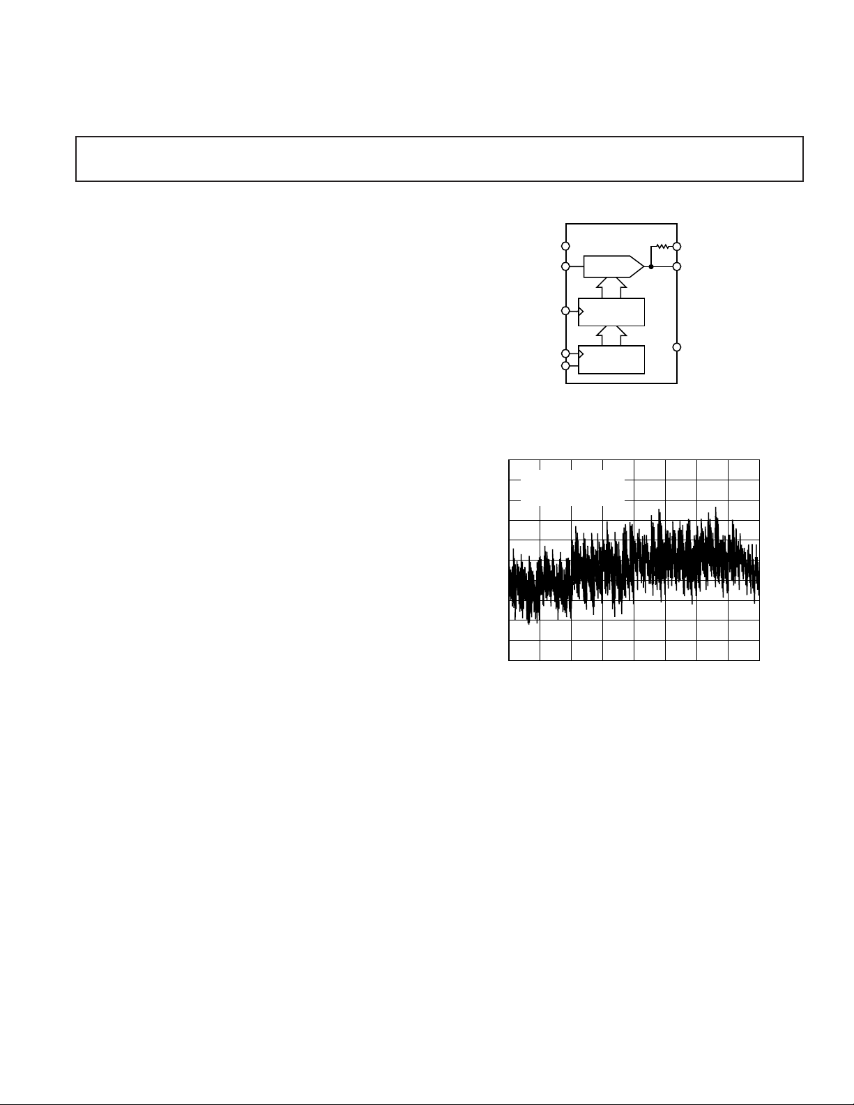
12-Bit Serial Input
CODE
INL – LSB
0.1
0
–0.1
0 1024 2048 3072 4096
–0.5
0.5
0.4
0.3
0.2
–0.2
–0.3
–0.4
512 1536 2560 3584
TA = +25ⴗC, +85ⴗC, –40ⴗC
V
DD
= +5V
V
REF
= –10V
a
FEATURES
Compact SO-8 and TSSOP Packages
True 12-Bit Accuracy
5 V Operation @ <10 A
Fast 3-Wire Serial Input
Fast 1 s Settling Time
2.4 MHz 4-Quadrant Multiply BW
Pin-for-Pin Upgrade for DAC8043
Standard and Rotated Pinout
APPLICATIONS
Ideal for PLC Applications in Industrial Control
Programmable Amplifiers and Attenuators
Digitally Controlled Calibration and Filters
Motion Control Systems
GENERAL DESCRIPTION
The DAC8043A is an improved high accuracy 12-bit multiplying digital-to-analog converter in space-saving 8-lead packages.
Featuring serial input, double buffering and excellent analog
performance, the DAC8043A is ideal for applications where PC
board space is at a premium. Improved linearity and gain error
performance permit reduced parts count through the elimination of trimming components. Separate input clock and load
DAC control lines allow full user control of data loading and
analog output.
The circuit consists of a 12-bit serial-in/parallel-out shift register, a 12-bit DAC register, a 12-bit CMOS DAC and control
logic. Serial data is clocked into the input register on the rising
edge of the CLOCK pulse. When the new data word has been
clocked in, it is loaded into the DAC register with the LD input
pin. Data in the DAC register is converted to an output current
by the D/A converter.
Consuming only 10 µA from a single 5 V power supply, the
DAC8043A is the ideal low power, small size, high performance
solution to many application problems.
The DAC8043A is specified over the extended industrial
(–40°C to +85°C) temperature range. DAC8043A is available
in plastic DIP, and the low profile 1.75 mm height SO-8 surface
mount packages. The DAC8043AFRU is available for ultracompact applications in a thin 1.1 mm TSSOP-8 package.
Multiplying D/A Converter
DAC8043A
FUNCTIONAL BLOCK DIAGRAM
V
DD
V
REF
LD
CLK
SRI
Figure 1. Integral Nonlinearity Error vs. Code
DAC8043A
DAC
12
DAC REG
12
12-BIT SHIFT
REGISTER
R
FB
I
OUT
GND
REV. A
Information furnished by Analog Devices is believed to be accurate and
reliable. However, no responsibility is assumed by Analog Devices for its
use, nor for any infringements of patents or other rights of third parties
which may result from its use. No license is granted by implication or
otherwise under any patent or patent rights of Analog Devices.
One Technology Way, P.O. Box 9106, Norwood, MA 02062-9106, U.S.A.
Tel: 781/329-4700 World Wide Web Site: http://www.analog.com
Fax: 781/326-8703 © Analog Devices, Inc., 2000

DAC8043A–SPECIFICATIONS
(@ V
ELECTRICAL CHARACTERISTICS
= 5 V, V
DD
Parameter Symbol Condition E Grade F Grade Unit
STATIC PERFORMANCE
Resolution N 12 12 Bits
Relative Accuracy INL ±0.5 ±1.0 LSB max
Differential Nonlinearity DNL All Grades Monotonic to 12 Bits ±0.5 ±1.0 LSB max
Gain Error
Gain Tempco
Output Leakage Current I
Zero-Scale Error
1
2
3
G
FSE
TCG
LKG
I
ZSE
TA = 25°C, Data = FFF
= –40°C, +85°C, Data = FFF
T
A
I
FS
Pin Measured ±5 ±5 ppm/°C max
OUT
Data = 000H, I
= –40°C, +85°C, Data = 000H, I
T
A
Data = 000
H
TA = –40°C, +85°C, Data = 000
REFERENCE INPUT
Input Resistance R
Input Capacitance
ANALOG OUTPUT
Output Capacitance
2
2
C
C
REF
REF
OUT
Absolute Tempco < 50 ppm/°C 7/15 7/15 kΩ min/max
Data = 000
Data = FFF
H
H
DIGITAL INPUTS
Digital Input Low V
Digital Input High V
Input Leakage Current I
Input Capacitance
INTERFACE TIMING
2
2, 4
Data Setup t
Data Hold t
Clock Width High t
Clock Width Low t
Load Pulsewidth t
LSB CLK to LD DAC t
AC CHARACTERISTICS
1, 2
Output Current Settling Time t
DAC Glitch Q Data = 000
Feedthrough (V
OUT/VREF
Total Harmonic Distortion THD V
Output Noise Density
)FT V
5
Multiplying Bandwidth BW –3 dB, V
C
e
IL
IH
IL
IL
DS
DH
CH
CL
LD
ASB
S
n
V
= 0 V to 5 V 0.001/±1 0.001/±1 µA typ/max
LOGIC
V
= 0 V 10 10 pF max
LOGIC
To ±0.01% of Full Scale, Ext Op Amp OP42 1 1 µs max
H
= 20 V p-p, Data = 000H, f = 10 kHz 1 1 mV p-p
REF
= 6 V rms, Data = FFFH, f = 1 kHz –85 –85 dB typ
REF
10 Hz to 100 kHz Between RFB and I
OUT/VREF
SUPPLY CHARACTERISTICS
Power Supply Range V
Positive Supply Current I
Power Dissipation P
DD RANGE
DD
DISS
V
LOGIC
V
LOGIC
= 0 V or V
= 0 V or V
Power Supply Sensitivity PSS ∆VDD = ±5% 0.002 0.002 %/% max
NOTES
1
Using internal feedback resistor RFB, see Figure 19 test circuit with V
2
These parameters are guaranteed by design and not subject to production testing.
3
Calculated from worst case R
4
All input control signals are specified with tR = tF = 2 ns (10% to 90% of 5 V) and timed from a voltage level of 1.6 V.
5
Calculation from en = √4KTRB where: K = Boltzmann Constant (J/°K), R = Resistance ( Ω), T = Resistor Temperature (°K), B = 1 Hz Bandwidth.
Specifications subject to change without notice.
REF
: I
ZSE
(LSB) = (R
REF
× I
× 4096)/V
LKG
REF
REF
= 10 V, –40ⴗC < TA < +85ⴗC, unless otherwise noted.)
REF
H
H
Pin Measured ±5 ±5 nA max
OUT
Pin Measured ±25 ±25 nA max
OUT
±1.0 ±2.0 LSB max
±2.0 ±2.0 LSB max
0.03 0.03 LSB max
H
0.15 0.15 LSB max
5 5 pF typ
25 25 pF typ
30 30 pF typ
0.8 0.8 V max
2.4 2.4 V min
10 10 ns min
5 5 ns min
25 25 ns min
25 25 ns min
25 25 ns min
0 0 ns min
to FFFH to 000H, V
, V
= 100 mV rms, Data = FFFH2.4 2.4 MHz typ
REF
= 0 V 20 20 nVs max
REF
OUT
17 17 nV/√Hz max
4.5/5.5 4.5/5.5 V min/max
DD
DD
= 10 V.
.
10 10 µA max
50 50 µW max
–2–
REV. A
DAC8043A
1
4
5
8
SO-8
DAC8043A
ES/FS
1
4
5
8
TSSOP-8
DAC8043A
FRU
TOP VIEW
(Not to Scale)
8
7
6
5
1
2
3
4
I
OUT
GND
LD
R
FB
V
REF
V
DD
CLK
SRI
PDIP-8
DAC8043A
EP/FP
TOP VIEW
(Not to Scale)
8
7
6
5
1
2
3
4
I
OUT
GND
LD
R
FB
V
REF
V
DD
CLKSRI
SO-8
DAC8043A1ES
DAC8043A1FS
WARNING!
ESD SENSITIVE DEVICE
ABSOLUTE MAXIMUM RATINGS*
VDD to GND . . . . . . . . . . . . . . . . . . . . . . . . . . . –0.3 V, +8 V
V
to GND . . . . . . . . . . . . . . . . . . . . . . . . . . . . . . . . ± 18 V
REF
to GND . . . . . . . . . . . . . . . . . . . . . . . . . . . . . . . . ±18 V
R
FB
Logic Inputs to GND . . . . . . . . . . . . . . –0.3 V, V
VI
to GND . . . . . . . . . . . . . . . . . . . –0.3 V, VDD + 0.3 V
OUT
Short Circuit to GND . . . . . . . . . . . . . . . . . . . . . 50 mA
I
OUT
Package Power Dissipation . . . . . . . . . . . . . (T
Thermal Resistance θ
JA
+ 0.3 V
DD
max – TA)/θ
J
JA
8-Lead Plastic DIP Package (N-8) . . . . . . . . . . . . 103°C/W
8-Lead SOIC Package (SO-8) . . . . . . . . . . . . . . . 158°C/W
TSSOP-8 Package (RU-8) . . . . . . . . . . . . . . . . . . 240°C/W
Maximum Junction Temperature (T
max) . . . . . . . . . 150°C
J
Operating Temperature Range . . . . . . . . . . – 40°C to +85°C
Storage Temperature Range . . . . . . . . . . . . –65°C to +150°C
Lead Temperature (Soldering, 10 sec) . . . . . . . . . . . . 300°C
*Stresses above those listed under Absolute Maximum Ratings may cause perma-
nent damage to the device. This is a stress rating only; functional operation of the
device at these or any other conditions above those indicated in the operational
sections of this specification is not implied. Exposure to absolute maximum rating
conditions for extended periods may affect device reliability.
ORDERING GUIDE
INL Package Package
Model (LSB) Temp Description Option
DAC8043AEP ±0.5 –40/+85°C 8-Lead P-DIP N-8
DAC8043AES ± 0.5 –40/+85°C 8-Lead SOIC SO-8
DAC8043A1ES ±0.5 –40/+85°C 8-Lead SOIC SO-8
DAC8043AFP ±1.0 –40/+85°C 8-Lead P-DIP N-8
DAC8043AFS ± 1.0 –40/+85°C 8-Lead SOIC SO-8
DAC8043A1FS ±1.0 –40/+85°C 8-Lead SOIC* SO-8
DAC8043AFRU ± 1.0 –40/+85°C TSSOP-8 RU-8
NOTES
The DAC8043A contains 346 transistors. The die size measures 70.3 mil ×
57.1 mil, 4014 sq mil.
*
The DAC8043A1ES and DAC8043A1FS have a rotated pinout.
TSSOP-8 Package Branding:
Line 1: yww (data code: year, work week).
Line 2: 8043A.
PIN FUNCTION DESCRIPTIONS
#(*) Name Function
1(7) V
DAC Reference Input Pin. Establishes DAC full-
REF
scale voltage. Constant input resistance versus
code.
2 (8) R
Internal Matching Feedback Resistor. Connect
FB
to external op amp output.
3 (1) I
DAC Current Output, full-scale output 1 LSB
OUT
less than reference input voltage –V
REF
.
4 (2) GND Analog and Digital Ground.
5 (3) LD Load Strobe, Level-Sensitive Digital Input.
Transfers shift-register data to DAC register
while active low. See truth table for operation.
6 (4) SRI 12-Bit Serial Register Input, data loads directly
into the shift register MSB first. Extra leading
bits are ignored.
7 (5) CLK Clock Input, positive-edge clocks data into shift
register.
8 (6) V
Positive Power Supply Input. Specified range of
DD
operation 5 V ± 10%.
*Note Pin numbers in parenthesis represent the rotated pinout of the
DAC8043A1ES and DAC8043A1FS models.
DAC8043AE/F PIN CONFIGURATIONS
DAC8043A1E AND DAC8043A1F PIN CONFIGURATION
(Rotated Pinout)
CAUTION
ESD (electrostatic discharge) sensitive device. Electrostatic charges as high as 4000 V readily
accumulate on the human body and test equipment and can discharge without detection.
Although the DAC8043A features proprietary ESD protection circuitry, permanent damage may
occur on devices subjected to high-energy electrostatic discharges. Therefore, proper ESD
precautions are recommended to avoid performance degradation or loss of functionality.
REV. A
–3–

DAC8043A
SRI
CLK
LD
D10 D9 D8 D6 D5 D4 D3 D2 D1 D0D7
D11
t
LD1
DATA LOADED MSB(D11) FIRST DAC REGISTER LOAD
t
ASB
t
CL
Dxx
tDS t
DH
t
CH
t
LD
t
S
ⴞ1 LSB
ERROR BAND
SRI
CLK
LD
FS
V
OUT
ZS
Figure 2. Timing Diagram
Table I. Control-Logic Truth Table
CLK LD Serial Shift Register Function DAC Register Function
u H Shift-Register-Data Advanced One Bit Latched
H or L L No Effect Updated with Current Shift Register Contents
L u No Effect Latched All 12 Bits
NOTES
u positive logic transition.
The DAC Register LD input is level-sensitive. Any time LD is logic-low data in the serial register will directly control the
switches in the R-2R DAC ladder.
Typical Performance Characteristics
35
SS = 200 UNITS
T
30
25
20
15
FREQUENCY
10
5
0
–1.0 1.0
–0.5 0.0 0.5
TOTAL UNADJUSTED ERROR – LSB
Figure 3. Total Unadjusted Error Histogram
V
V
= 25ⴗC
A
= 5V
DD
REF
= 10V
–4–
50
SS = 200 UNITS
T
= –40ⴗC TO +85ⴗC
A
V
= 5V
DD
40
V
= 10V
REF
30
20
FREQUENCY
10
0
0
12
FULL SCALE TEMPCO – ppm/ⴗC
Figure 4. Full-Scale Output Tempco Histogram
REV. A

0.5
FREQUENCY – Hz
PSRR – dB
20
10k
⌬ VDD = 5V ⴞ10%
100k 1M 10M
40
60
80
100
1k
OPAMP OFFSET VOS – V
INL – LSB
–1000 0 1000 2000–2000
2
0
4
VDD = 5V
V
REF
= 10V
T
A
= 25ⴗC
–4
–2
DAC8043A
0.4
– mA
DD
0.3
0.2
SUPPLY CURRENT I
0.1
0
0.5 1.5 2.5 3.5 4.5
0
12 345
LOGIC INPUT VOLTAGE – Volts
TA = 25ⴗC
V
= 5V
DD
Figure 5. Supply Current vs. Logic Input Voltage
10
VDD = 5V
V
= 0V OR V
0.1
– A
DD
I
0.01
0.001
LOGIC
–35 –15 5 25 45165 85 105 125
–55
DD
TEMPERATURE – ⴗC
Figure 6. Supply Current vs. Temperature
Figure 8. Power Supply Rejection vs. Frequency
0.5
0.4
VDD = 5V
V
= 10V
REF
DNL – LSB
–0.1
–0.2
–0.3
–0.4
–0.5
0.3
0.2
0.1
0
0
SUPERIMPOSED: T
512 1536 2560 3584
= –40ⴗC, +25ⴗC, +85ⴗC
A
1024 2048 3072 4096
CODE – Decimal
Figure 9. Linearity Error vs. Digital Code
3500
VDD = 5V
3000
2500
2000
– A
DD
I
1500
1000
500
0
Figure 7. Supply Current vs. Clock Frequency
REV. A
= 10V
V
REF
= 25ⴗC
T
A
CODE = 800H
CODE = FFFH
10k
100k 1M 10M
FREQUENCY – Hz
CODE = F55H
100M1k
Figure 10. Linearity Error vs. External Op Amp V
OS
–5–

DAC8043A
–95
10
0.0018
1k 10k 100k
THD – %
100
0.0032
0.0056
0.010
0.018
0.032
–90
–85
–80
–75
–70
V
REF
= 4V p-p
OUTPUT OP AMP: OP42
THD – dB
FREQUENCY – Hz
VDD = 5V
V
= 10V
REF
f
V
OUT
(10mV/DIV)
LD
(5V/DIV)
20mV
TIME – 200ns/DIV
= 2.5MHz
CLK
CODE: 7FF
TO 800
H
H
Figure 11. Midscale Transition Performance
5V
CLK
(5V/DIV)
VDD = 5V
= 10V
V
REF
= 25ⴗC
T
A
0.5
0.25
INL – LSB
–0.25
–0.5
0
0
5
|V
| – Volts
REF
VDD = 5V
T
= 25ⴗC
A
10
Figure 14. Linearity Error vs. Reference Voltage
1.2
SAMPLE SIZE = 50
1.0
0.8
0.6
CODE = FFF
H
ALL BITS ON
V
OUT
(5V/DIV)
5V
TIME – 1s/DIV
Figure 12. Large Signal Settling Time
(MSB) B
11
B
10
B
9
B
8
B
7
B
6
B
5
B
4
B
3
B
2
B
DATA BITS "ON"
Figure 13. Reference Multiplying Bandwidth vs. Fre-
1
(LSB) B
0
(ALL OTHER DATA BITS "OFF")
100
1k 10k 100k 1M 10M
ALL BITS OFF
FREQUENCY – Hz
0
12
24
36
48
60
72
84
96
108
quency and Code
ATTENUATION – dB
0.4
NOMINAL CHANGE IN VOLTAGE – mV
0.2
CODE = 000
0
100 200 300 400 500 600
0
HOURS OF OPERATION AT 150ⴗC
H
Figure 15. Long-Term Drift Accelerated by Burn-In
Figure 16. THD vs. Frequency
–6–
REV. A

DAC8043A
PARAMETER DEFINITIONS
INTEGRAL NONLINEARITY (INL)
This is the single most important DAC specification. ADI measures INL as the maximum deviation of the analog output (from
the ideal) from a straight line drawn between the end points. It
is expressed as a percent of full-scale range or in terms of LSBs.
Refer to Analog Devices Data Reference Manual for additional
digital-to-analog converter definitions.
INTERFACE LOGIC INFORMATION
The DAC8043A has been designed for ease of operation. The
timing diagram, Figure 2, illustrates the input register loading
sequence. Note that the most significant bit (MSB) is loaded
first. Once the 12-bit input register is full, the data is transferred
to the DAC register by taking LD momentarily low.
DIGITAL SECTION
The DAC8043A’s digital inputs, SRI, LD, and CLK, are TTL
compatible. The input voltage levels affect the amount of current drawn from the supply; peak supply current occurs as the
digital input (VIN) passes through the transition region. See the
Supply Current vs. Logic Input Voltage graph located in the
typical performance characteristics curves. Maintaining the
digital input voltage levels as close as possible to the supplies,
VDD and GND, minimizes supply current consumption. The
DAC8043A’s digital inputs have been designed with ESD resistance incorporated through careful layout and the inclusion of
input protection circuitry. Figure 17 shows the input protection
diodes and series resistor; this input structure is duplicated on
each digital input. High voltage static charges applied to the
inputs are shunted to the supply and ground rails through forward biased diodes. These protection diodes were designed to
clamp the inputs to well below dangerous levels during static
discharge conditions.
V
DD
LD, CLK, SRI
5k⍀
code. This constant current results in a constant input resistance at V
equal to R. The V
REF
input may be driven by any
REF
reference voltage or current, ac or dc that is within the limits
stated in the Absolute Maximum Ratings.
V
REF
(SWITCHES SHOWN FOR DIGITAL INPUTS "HIGH")
*THESE SWITCHES PERMANENTLY "ON"
10k⍀
20k⍀S220k⍀
S1
BIT 1 (MSB) BIT 2 BIT 3 BIT 12 (LSB)
10k⍀
DIGITAL INPUTS
20k⍀
S3
10k⍀
20k⍀
S12
20k⍀
*
*
10k⍀
GND
I
OUT
R
FEEDBACK
Figure 18. Simplified DAC Circuit
The twelve output current steering NMOS FET switches are in
series with each R-2R resistor.
To further ensure accuracy across the full temperature range,
permanently “ON” MOS switches were included in series with
the feedback resistor and the R-2R ladder’s terminating resistor.
Figure 18 shows the location of the series switches. During any
testing of the resistor ladder or R
inspection), V
must be present to turn “ON” these series
DD
FEEDBACK
(such as incoming
switches.
DYNAMIC PERFORMANCE
OUTPUT IMPEDANCE
The DAC8043A’s output resistance, as in the case of the output
capacitance, varies with the digital input code. This resistance,
looking back into the I
terminal, may be between 10 kΩ (the
OUT
feedback resistor alone when all digital inputs are LOW) and
7.5 kΩ (the feedback resistor in parallel with approximate 30 kΩ
of the R-2R ladder network resistance when any single bit logic
is HIGH). Static accuracy and dynamic performance will be
affected by these variations.
GND
Figure 17. Digital Input Protection
GENERAL CIRCUIT INFORMATION
The DAC8043A is a 12-bit multiplying D/A converter with a
very low temperature coefficient. It contains an R-2R resistor
ladder network, data input and control logic, and two data
registers.
The digital circuitry forms an interface in which serial data can
be loaded under microprocessor control into a 12-bit shift register and then transferred, in parallel, to the 12-bit DAC register.
The analog portion of the DAC8043A contains an inverted
R-2R ladder network consisting of silicon-chrome, highly-stable
(50 ppm/°C) thin-film resistors, and twelve pairs of NMOS
current-steering switches, see Figure 18. These switches steer
binarily weighted currents into either I
or GND; this yields a
OUT
constant current in each ladder leg, regardless of digital input
REV. A
–7–
APPLICATIONS INFORMATION
In most applications, linearity depends upon the potential of the
I
and GND pins being at the same voltage potential. The
OUT
DAC is connected to an external precision op amp inverting
input. The external amplifiers noninverting input should be tied
directly to ground without the usual bias current compensating
resistor. (See Figures 19 and 20.) The selected amplifier should
have a low input bias current and low drift over temperature.
The amplifiers input offset voltage should be nulled to less than
200 microvolts (less than 10% of 1 LSB). All grounded pins
should tie to a single common ground point to avoid ground loops.
The V
power supply should have a low noise level with
DD
adequate bypassing. It is best to operate the DAC8043A from
the analog power supply and grounds.

DAC8043A
UNIPOLAR 2-QUADRANT MULTIPLYING
The most straightforward application of the DAC8043A is in
the 2-quadrant multiplying configuration shown in Figure 19. If
the reference input signal is replaced with a fixed dc voltage
reference, the DAC output will provide a proportional dc voltage
output according to the transfer equation:
V
= –D/4096 × V
OUT
REF
where D is the decimal data loaded into the DAC register and
V
is the externally applied reference voltage source.
REF
V
DD
R
R
FB
FB
GND
10pF
I
OUT
OP77
V
OUT
2R
ⴞ10V
V
REF
V
AC
P
R
2R
DIGITAL INPUTS OMITTED FOR CLARITY
Figure 19. Unipolar (2-Quadrant) Operation
BIPOLAR 4-QUADRANT MULTIPLYING
Figure 20 shows a suggested circuit to achieve 4-quadrant multiplying operation. The summing amplifier multiplies V
OUT1
by
2, and offsets the output with the reference voltage so that a
midscale digital input code of 2048 places V
at zero volts.
OUT2
The negative full-scale voltage will be V
when the DAC is
REF
loaded with all zeros. The positive full-scale output will be
– 1 LSB) when the DAC is loaded with all ones. Thus
–(V
REF
the digital coding is offset binary. The voltage output transfer
equation for various input data and reference (or signal) values
follows:
V
= (D/2048 – 1) × –V
OUT2
REF
where D is the decimal data loaded into the DAC register and
V
is the externally applied reference voltage source.
REF
Precision resistors will be necessary to avoid ratio errors. Otherwise trimming will be required to achieve full accuracy specifications available from the DAC8043A device. See the various
Analog Devices Digital Potentiometer products for automated
trimming solutions (e.g., the AD5204 for low voltage applications or the AD7376 for high voltage applications).
V
V
REF
V
AC
ⴞ10V
P
DIGITAL INPUTS OMITTED FOR CLARITY
DD
R
R
2R
FB
2R
R
FB
GND
I
OUT
10pF
OP213
(0V TO –V
20k⍀ 20k⍀
10k⍀
V
OUT1
OP213
)
REF
V
OUT2
Figure 20. Bipolar (4-Quadrant) Operation
C00272–0–10/00 (rev. A)
0.210 (5.33)
MAX
0.160 (4.06)
0.115 (2.93)
0.022 (0.558)
0.014 (0.356)
8-Lead Plastic DIP (N-8)
0.430 (10.92)
0.348 (8.84)
8
14
PIN 1
0.100
(2.54)
BSC
5
0.280 (7.11)
0.240 (6.10)
0.060 (1.52)
0.015 (0.38)
0.070 (1.77)
0.045 (1.15)
0.130
(3.30)
MIN
SEATING
PLANE
0.325 (8.25)
0.300 (7.62)
0.015 (0.381)
0.008 (0.204)
PIN 1
0.006 (0.15)
0.002 (0.05)
SEATING
PLANE
OUTLINE DIMENSIONS
Dimensions shown in inches and (mm).
0.1574 (4.00)
0.1497 (3.80)
0.195 (4.95)
0.115 (2.93)
0.0098 (0.25)
0.0040 (0.10)
8-Lead TSSOP (RU-8)
0.122 (3.10)
0.114 (2.90)
8
5
0.177 (4.50)
0.169 (4.30)
1
0.0256 (0.65)
BSC
0.0118 (0.30)
0.0075 (0.19)
4
0.256 (6.50)
0.246 (6.25)
0.0433
(1.10)
MAX
0.0079 (0.20)
0.0035 (0.090)
8ⴗ
0ⴗ
PIN 1
SEATING
PLANE
0.028 (0.70)
0.020 (0.50)
8-Lead SOIC (SO-8)
0.1968 (5.00)
0.1890 (4.80)
8
5
0.2440 (6.20)
41
0.2284 (5.80)
0.0688 (1.75)
0.0532 (1.35)
0.0500
(1.27)
BSC
0.0192 (0.49)
0.0138 (0.35)
0.0098 (0.25)
0.0075 (0.19)
0.0196 (0.50)
0.0099 (0.25)
8°
0°
0.0500 (1.27)
0.0160 (0.41)
x 45°
PRINTED IN U.S.A.
–8–
REV. A
 Loading...