Analog Devices AD7841 a Datasheet

Octal 14-Bit, Parallel Input,
a
FEATURES
Eight 14-Bit DACs in One Package
Voltage Outputs
Offset Adjust for Each DAC Pair
Reference Range of 5 V
Maximum Output Voltage Range of 10 V
15 V 10% Operation
Clear Function to User-Defined Voltage
44-Lead MQFP Package
APPLICATIONS
Automatic Test Equipment
Process Control
General Purpose Instrumentation
V
CCVSSVDD
GENERAL DESCRIPTION
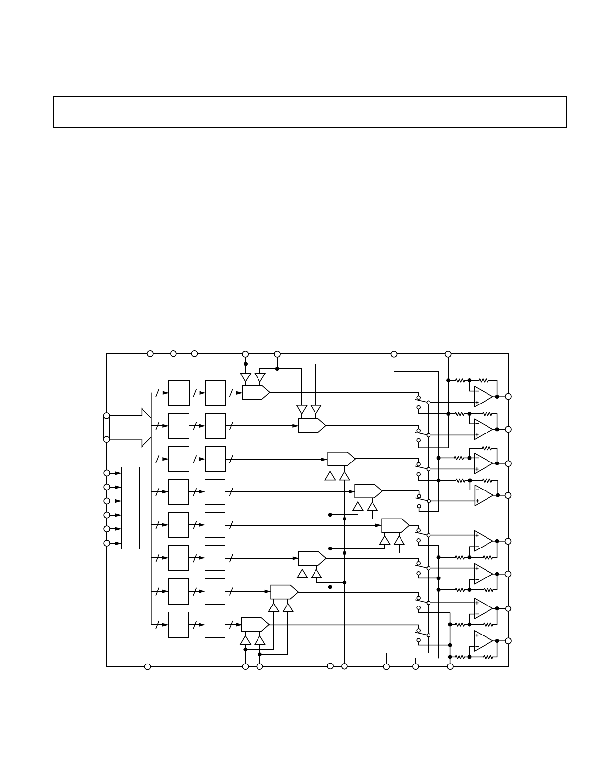
The AD7841 contains eight 14-bit DACs on one monolithic
chip. It has output voltages with a full-scale range of ±10 V
from reference voltages of ±5 V.
The AD7841 accepts 14-bit parallel loaded data from the external bus into one of the input registers under the control of the
WR, CS, and DAC channel address pins, A0–A2.
The DAC outputs are updated on reception of new data into
the DAC registers. All the outputs may be updated simultaneously by taking the LDAC input low.
Each DAC output is buffered with a gain-of-two amplifier into
which an external DAC offset voltage can be inserted via the
DUTGNDx pins.
The AD7841 is available in a 44-lead MQFP package.
FUNCTIONAL BLOCK DIAGRAM
V
REF
(+)ABV
REF
(–)
AB
DUTGND
CD
Voltage-Output DAC
AD7841
DUTGND
AB
DB13
DB0
WR
CS
A0
LDAC
AD7841
14 14 14
INPUT
REG
A
14 14 14
INPUT
REG
B
14 14 14
INPUT
REG
C
14 14 14
INPUT
REG
D
A1
A2
14 14 14
DECODE
ADDRESS
INPUT
REG
E
14 14 14
INPUT
REG
F
14 14 14
INPUT
REG
G
14
INPUT
REG
H
DAC
REG
A
DAC
REG
B
DAC
REG
C
DAC
REG
D
DAC
REG
E
DAC
REG
F
DAC
REG
G
14 14
DAC
REG
H
DAC A
DAC B
DAC C
DAC D
DAC E
DAC F
DAC G
DAC H
RR
RR
R
R
R
R
R
R
R
R
R
R
R
R
A
V
OUT
B
V
OUT
C
V
OUT
D
V
OUT
E
V
OUT
F
V
OUT
G
V
OUT
H
V
OUT
V
GND
V
REF
GH
(–)
(+)
REF
GH
REV. A
Information furnished by Analog Devices is believed to be accurate and
reliable. However, no responsibility is assumed by Analog Devices for its
use, nor for any infringements of patents or other rights of third parties
which may result from its use. No license is granted by implication or
otherwise under any patent or patent rights of Analog Devices.
V
REF
CDEF
(–)
(+)
V
REF
CDEF
CLR
DUTGND
EF
DUTGND
GH
One Technology Way, P.O. Box 9106, Norwood, MA 02062-9106, U.S.A.
Tel: 781/329-4700 World Wide Web Site: http://www.analog.com
Fax: 781/326-8703 © Analog Devices, Inc., 2000

(VCC = 5 V 5%; VDD = 15 V 10%; VSS = –15 V 10%; GND = DUTGND =
AD7841–SPECIFICATIONS
0 V; RL = 5 k and CL = 50 pF to GND, T
Parameter A B Unit Test Conditions/Comments
ACCURACY
Resolution 14 14 Bits
Relative Accuracy ±4 ±2 LSB max
Differential Nonlinearity –0.9/2 ±1 LSB max Guaranteed Monotonic Over Temperature for All
Zero-Scale Error ±8 ±8 LSB max V
Full-Scale Error ±8 ±8 LSB max V
Gain Error ±2 ±2 LSB typ V
Gain Temperature Coefficient
DC Crosstalk
REFERENCE INPUTS
2
2
2
0.5 0.5 ppm FSR/°C typ
10 10 ppm FSR/°C max
120 120 µV max See Terminology. Typically 75 µV
DC Input Impedance 100 100 MΩ typ
Input Current ±1 ±1 µA max Per Input. Typically ± 0.03 µA
(+) Range 0/5 0/5 V min/max
V
REF
V
(–) Range –5/0 –5/0 V min/max
REF
(+) – V
[V
REF
DUTGND INPUTS
(–)] 2/10 2/10 V min/max For Specified Performance. Can Go as Low as 0 V,
REF
2
DC Input Impedance 60 60 kΩ typ
Max Input Current ±0.3 ±0.3 mA typ Per Input
Input Range
OUTPUT CHARACTERISTICS
3
–2/+2 –2/+2 V min/max
2
Output Voltage Swing VSS + 2.5 V to VSS + 2.5 V to V typ V
– 2.5 V VDD – 2.5 V – V
V
DD
Short Circuit Current 15 15 mA max
Resistive Load 5 5 kΩ min To 0 V
Capacitive Load 50 50 pF max To 0 V
DC Output Impedance 0.5 0.5 Ω max
DIGITAL INPUTS
V
, Input High Voltage 2.4 2.4 V min
INH
, Input Low Voltage 0.8 0.8 V max
V
INL
I
, Input Current Total for All Pins
INH
2
@ 25°C ±1 ±1 µA max
to T
T
MIN
MAX
±10 ±10 µA max
CIN, Input Capacitance 10 10 pF max
POWER REQUIREMENTS
V
CC
V
DD
V
SS
Power Supply Sensitivity
∆Full Scale/∆V
∆Full Scale/∆V
I
CC
I
DD
I
SS
NOTES
1
Temperature range for A and B Versions: –40°C to +85°C.
2
Guaranteed by characterization. Not production tested.
3
See DUTGND Voltage Range section.
4
The AD7841 is functional with power supplies of ± 12 V ± 10% with reduced output range. Output amplifier requires 2.5 V of head room at the bottom and top ends
of the transfer for function. At 12 V supplies it is recommended to restrict the reference range to ±4 V.
Specifications subject to change without notice.
DD
SS
4
4.75/+5.25 4.75/+5.25 V min/max For Specified Performance
15 V ± 10% 15 V ± 10% V min/max For Specified Performance
2
–15 V ± 10% –15 V ± 10% V min/max For Specified Performance
90 90 dB typ
90 90 dB typ
0.5 0.5 mA max V
10 10 mA max Outputs Unloaded. Typically 8 mA
10 10 mA max Outputs Unloaded. Typically 8 mA
1
= T
to T
A
MIN
, unless otherwise noted)
MAX
Grades
(+) = +5 V, V
REF
(–) = –5 V. Typically within
REF
±2 LSB
(+) = +5 V, V
REF
(–) = –5 V. Typically within
REF
±2 LSB
(+) = +5 V, V
REF
(–) = –5 V
REF
but Performance Not Guaranteed
= 2 × (V
OUT
DUTGND
= VCC, V
INH
(–) + [V
REF
= GND. Dynamic Current
INL
REF
(+) – V
(–)] × D)
REF
–2–
REV. A

AD7841
(These characteristics are included for Design Guidance and are not subject
AC PERFORMANCE CHARACTERISTICS
A & B
Parameter Versions Unit Test Conditions/Comments
DYNAMIC PERFORMANCE
Output Voltage Settling Time 31 µs typ Full-Scale Change to ±1/2 LSB. DAC Latch Contents Alternately
Slew Rate 0.7 V/µs typ
Digital-to-Analog Glitch Impulse 230 nV-s typ Measured with V
Channel-to-Channel Isolation 99 dB typ See Terminology
DAC-to-DAC Crosstalk 40 nV-s typ See Terminology
Digital Crosstalk 0.2 nV-s typ Feedthrough to DAC Output Under Test Due to Change in Digital
Digital Feedthrough 0.1 nV-s typ Effect of Input Bus Activity on DAC Output Under Test
Output Noise Spectral Density
@ 1 kHz 200 nV/√Hz typ All 1s Loaded to DAC. V
Specifications subject to change without notice.
1, 2
TIMING SPECIFICATIONS
(VCC = 5 V 5%; VDD = 15 V 10%; VSS = –15 V 10%; GND = DUTGND = 0 V)
to production testing.)
Loaded with All 0s and All 1s
(+) = +5 V, V
REF
(–) = –5 V. DAC Latch
REF
Alternately Loaded with 1FFF Hex and 2000 Hex. Not Dependent
on Load Conditions
Input Code to Another Converter
(+) = V
REF
(–) = 0 V
REF
Parameter Limit at T
t
1
t
2
t
3
t
4
t
5
t
6
t
7
t
8
t
9
t
10
t
11
NOTES
1
All input signals are specified with tr = tf = 5 ns (10% to 90% of 5 V) and timed from a voltage level of 1.6 V.
2
Rise and fall times should be no longer than 50 ns.
Specifications subject to change without notice.
15 ns min Address to WR Setup Time
0 ns min Address to WR Hold Time
50 ns min CS Pulsewidth Low
50 ns min WR Pulsewidth Low
0 ns min CS to WR Setup Time
0 ns min WR to CS Hold Time
20 ns min Data Setup Time
0 ns min Data Hold Time
31 µs typ Settling Time
300 ns max CLR Pulse Activation Time
50 ns min LDAC Pulsewidth Low
A0, A1, A2
DATA
V
CS
WR
OUT
CLR
MIN, TMAX
t
1
t
5
t
2
t
6
t
3
t
4
t
8
t
7
t
9
t
10
Unit Description
V
OUT
LDAC
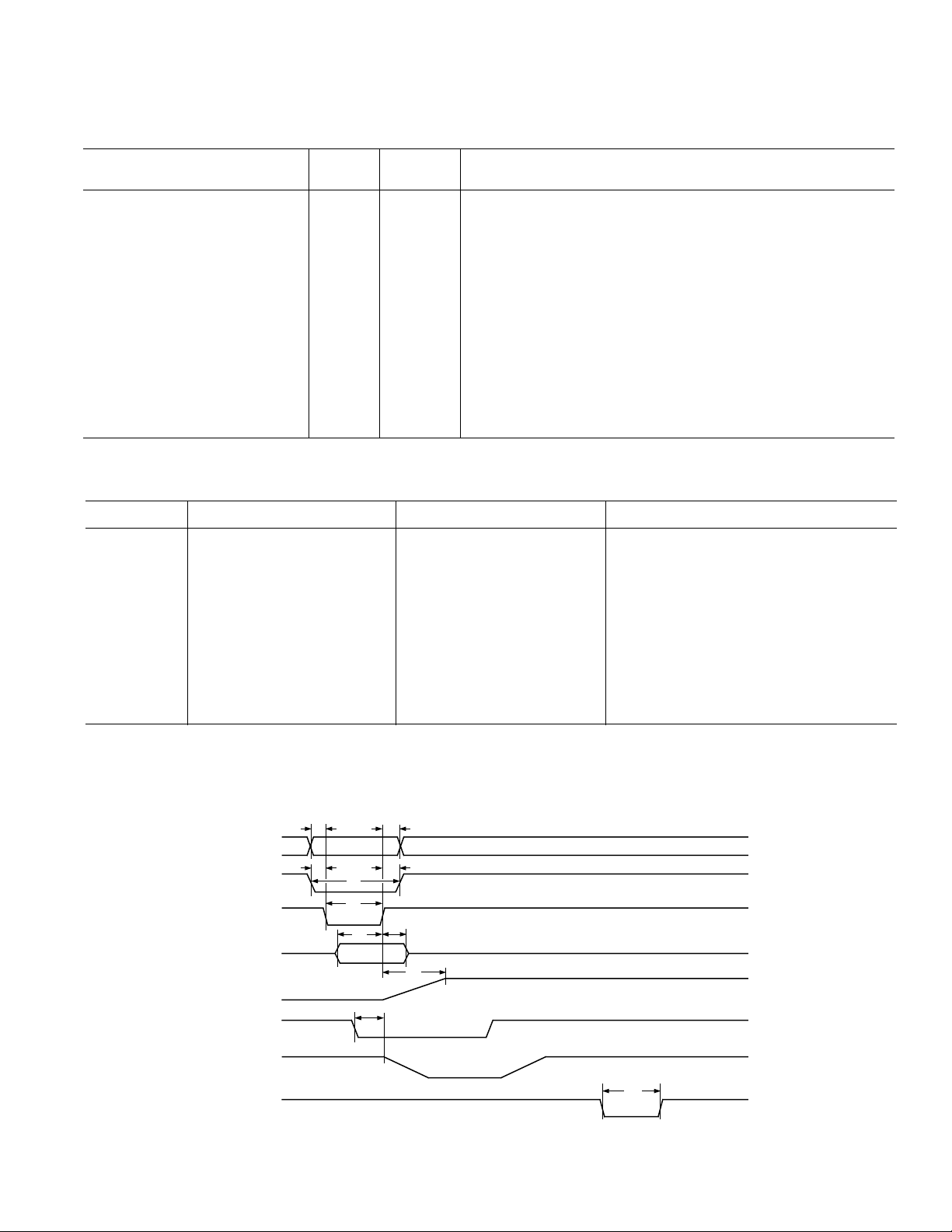
Figure 1. Timing Diagram
–3–REV. A
t
11

AD7841
V
DD
V
CC
AD7841
HP5082-2811
V
DD
V
CC
IN4148
ABSOLUTE MAXIMUM RATINGS
1, 2
(TA = 25°C unless otherwise noted)
VCC to GND3 . . . . . . . . . . . . . . –0.3 V, +7 V or V
+ 0.3 V
DD
(Whichever Is Lower)
to GND . . . . . . . . . . . . . . . . . . . . . . . . . . . –0.3 V, +17 V
V
DD
V
to GND . . . . . . . . . . . . . . . . . . . . . . . . . . . . +0.3 V, –17 V
SS
Digital Inputs to GND . . . . . . . . . . . . . . –0.3 V, V
(+) to V
V
REF
V
(+) to GND . . . . . . . . . . . . . . . VSS – 0.3 V, VDD + 0.3 V
REF
V
(–) to GND . . . . . . . . . . . . . . . VSS – 0.3 V, VDD + 0.3 V
REF
DUTGND to GND . . . . . . . . . . . . . V
V
(A–H) to GND . . . . . . . . . . . . VSS – 0.3 V, VDD + 0.3 V
OUT
(–) . . . . . . . . . . . . . . . . . . . . . –0.3 V, +18 V
REF
– 0.3 V, VDD + 0.3 V
SS
+ 0.3 V
CC
Operating Temperature Range
Industrial (A Version) . . . . . . . . . . . . . . . –40°C to +85°C
Storage Temperature Range . . . . . . . . . . . . –65°C to +150°C
ORDERING GUIDE
Linearity
Temperature Error DNL Package Package
Model Range (LSBs) (LSBs) Description Option
AD7841AS –40°C to +85°C ± 4 –0.9/+2 Plastic Quad Flatpack (MQFP) S-44
AD7841BS –40°C to +85°C ±2 ±1 Plastic Quad Flatpack (MQFP) S-44
Junction Temperature . . . . . . . . . . . . . . . . . . . . . . . . . 150°C
MQFP Package
Power Dissipation . . . . . . . . . . . . . . . . . (T
Max – TA)/θ
J
JA
θJA Thermal Impedance . . . . . . . . . . . . . . . . . . . . . 95°C/W
Lead Temperature, Soldering
Vapor Phase (60 sec) . . . . . . . . . . . . . . . . . . . . . . . . 215°C
Infrared (15 sec) . . . . . . . . . . . . . . . . . . . . . . . . . . . 220°C
ESD . . . . . . . . . . . . . . . . . . . . . . . . . . . . . . . . . . . . . >4000 V
NOTES
1
Stresses above those listed under Absolute Maximum Ratings may cause perma-
nent damage to the device. This is a stress rating only; functional operation of the
device at these or any other conditions above those indicated in the operational
section of this specification is not implied. Exposure to absolute maximum rating
conditions for extended periods may affect device reliability.
2
Transient currents of up to 100 mA will not cause SCR latch-up.
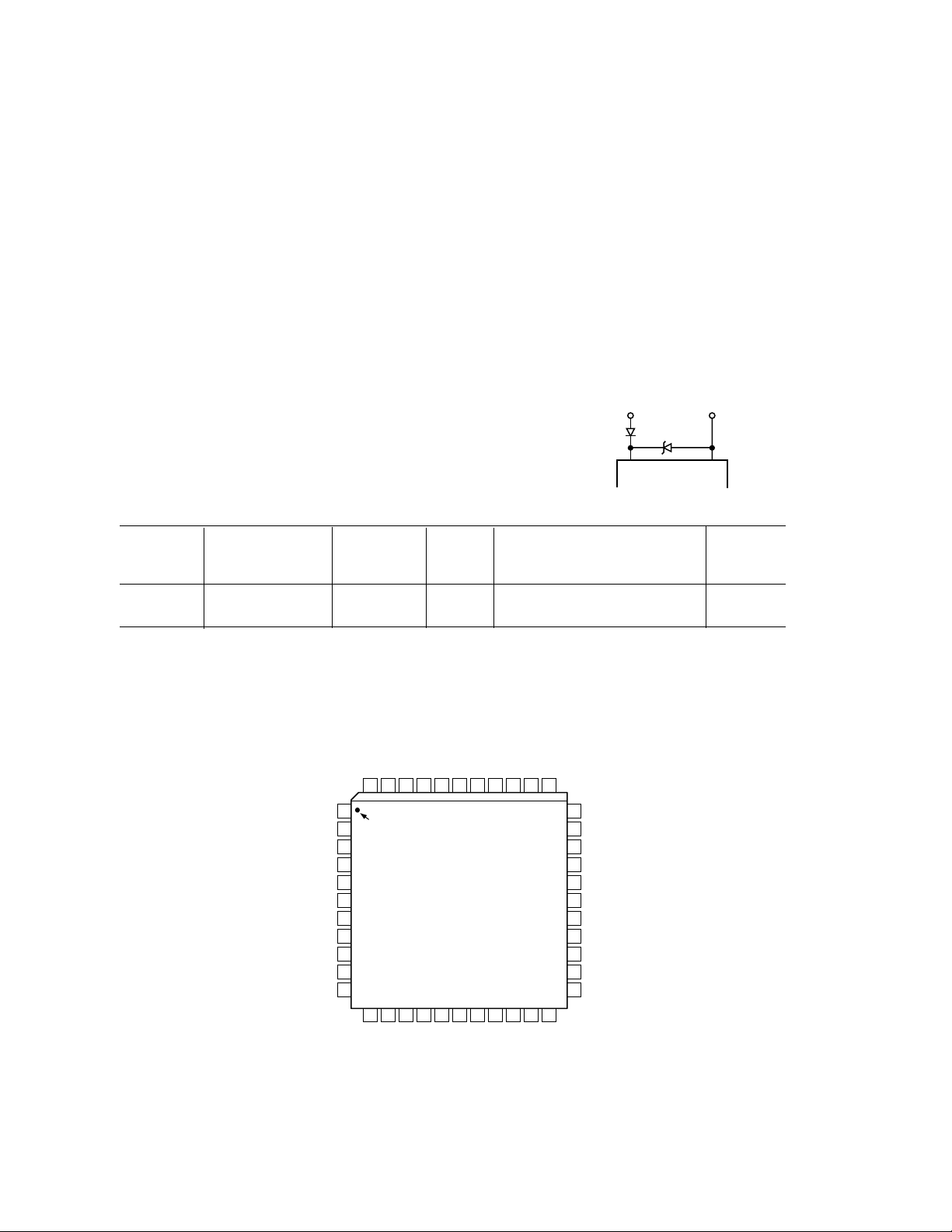
3
VCC must not exceed VDD by more than 0.3 V. If it is possible for this to happen
during power supply sequencing, the following diode protection scheme will ensure
protection.
DUTGND_AB
V
OUT
V
(–)AB
REF
V
(+)AB
REF
V
DD
V
LDAC
A2
A1
A0
CS
PIN CONFIGURATION
C
OUT
V
DUTGND_CD
CC
V
GND
D
(–)CDEF
OUT
REF
V
V
40 39 3841424344 36 35 3437
AD7841
TOP VIEW
(Not to Scale)
DB1
DB0
B
OUT
V
1
PIN 1
IDENTIFIER
2
A
3
4
5
6
SS
7
8
9
10
11
12 13 14 15 16 1 7 18 19 20 21 22
WR
(+)CDEF
DD
REF
V
V
DB3
DB2
E
OUT
V
DUTGND_EF
DB5
DB4
F
OUT
V
DB6
G
OUT
V
DB7
33
32
31
30
29
28
27
26
25
24
23
DUTGND_GH
H
V
OUT
V
(–)GH
REF
(+)GH
V
REF
CLR
DB13
DB12
DB11
DB10
DB9
DB8
–4–
REV. A
 Loading...