

Octal 14-Bit, Parallel Input,
a
FEATURES
Eight 14-Bit DACs in One Package
Voltage Outputs
Offset Adjust for Each DAC Pair
Reference Range of ⴞ5 V
Maximum Output Voltage Range of ⴞ10 V
ⴞ15 V ⴞ 10% Operation
Clear Function to User-Defined Voltage
44-Lead MQFP Package
APPLICATIONS
Automatic Test Equipment
Process Control
General Purpose Instrumentation
V
CCVSSVDD
GENERAL DESCRIPTION
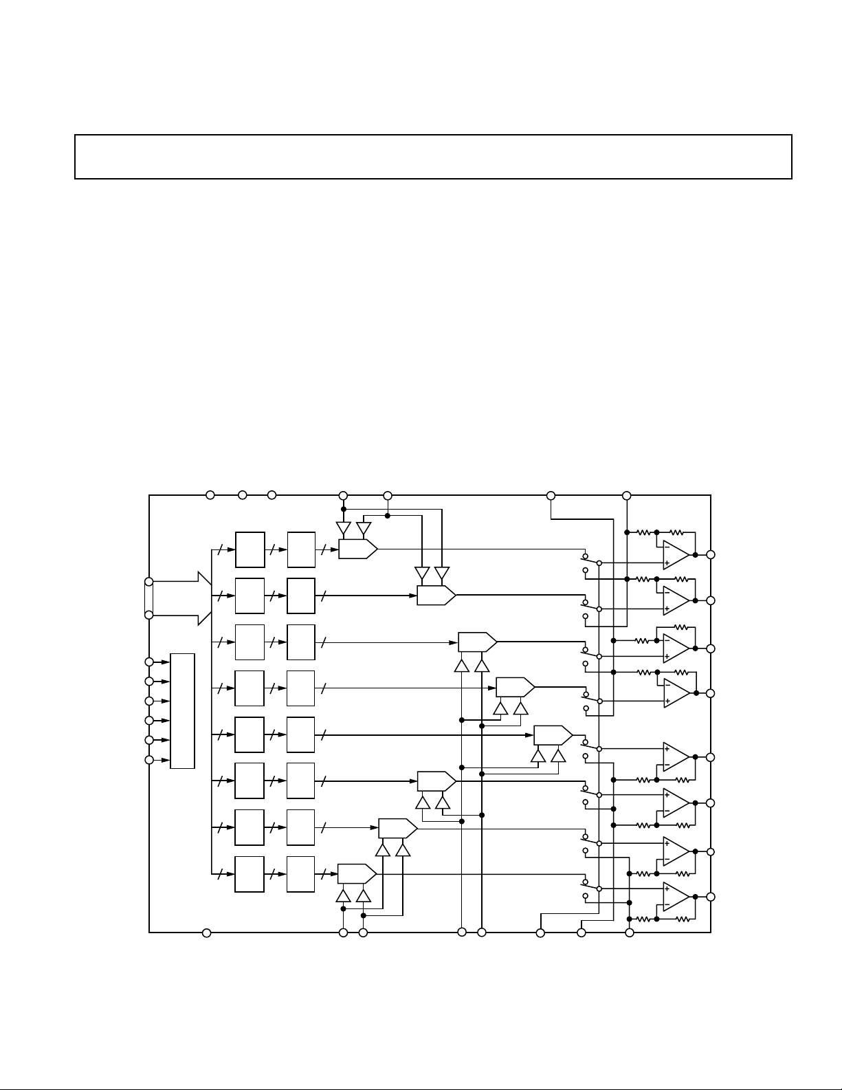
The AD7841 contains eight 14-bit DACs on one monolithic
chip. It has output voltages with a full-scale range of ±10 V
from reference voltages of ±5 V.
The AD7841 accepts 14-bit parallel loaded data from the external bus into one of the input registers under the control of the
WR, CS and DAC channel address pins, A0–A2.
The DAC outputs are updated on reception of new data into
the DAC registers. All the outputs may be updated simultaneously by taking the LDAC input low.
Each DAC output is buffered with a gain-of-two amplifier into
which an external DAC offset voltage can be inserted via the
DUTGNDx pins.
The AD7841 is available in a 44-lead MQFP package.
FUNCTIONAL BLOCK DIAGRAM
V
REF
(+)ABV
REF
(–)
AB
DUTGND
CD
Voltage-Output DAC
AD7841
DUTGND
AB
DB13
DB0
WR
CS
A0
LDAC
AD7841
14 14 14
INPUT
REG
A
14 14 14
INPUT
REG
B
14 14 14
INPUT
REG
C
14 14 14
INPUT
REG
D
A1
A2
14 14 14
DECODE
ADDRESS
INPUT
REG
E
14 14 14
INPUT
REG
F
14 14 14
INPUT
REG
G
14
INPUT
REG
H
DAC
REG
A
DAC
REG
B
DAC
REG
C
DAC
REG
D
DAC
REG
E
DAC
REG
F
DAC
REG
G
14 14
DAC
REG
H
DAC A
DAC B
DAC C
DAC D
DAC E
DAC F
DAC G
DAC H
RR
RR
R
R
R
R
R
R
R
R
R
R
R
R
A
V
OUT
B
V
OUT
C
V
OUT
D
V
OUT
E
V
OUT
F
V
OUT
G
V
OUT
H
V
OUT
V
GND
V
REF
GH
(–)
(+)
REF
GH
REV. 0
Information furnished by Analog Devices is believed to be accurate and
reliable. However, no responsibility is assumed by Analog Devices for its
use, nor for any infringements of patents or other rights of third parties
which may result from its use. No license is granted by implication or
otherwise under any patent or patent rights of Analog Devices.
V
REF
CDEF
(–)
(+)
V
REF
CDEF
CLR
DUTGND
EF
DUTGND
GH
One Technology Way, P.O. Box 9106, Norwood, MA 02062-9106, U.S.A.
Tel: 781/329-4700 World Wide Web Site: http://www.analog.com
Fax: 781/326-8703 © Analog Devices, Inc., 1999
(VCC = +5 V ⴞ 5%; VDD = +15 V ⴞ 10%; VSS = –15 V ⴞ 10%; GND = DUTGND =
AD7841–SPECIFICATIONS
0 V; RL = 5 k⍀ and CL = 50 pF to GND, T
Parameter A B Units Test Conditions/Comments
ACCURACY
Resolution 14 14 Bits
Relative Accuracy ±4 ±2 LSB max
Differential Nonlinearity –0.9/2 ±1 LSB max Guaranteed Monotonic Over Temperature for All
Zero-Scale Error ±8 ±8 LSB max V
Full-Scale Error ±8 ±8 LSB max V
Gain Error ±2 ±2 LSB typ V
Gain Temperature Coefficient
DC Crosstalk
REFERENCE INPUTS
2
2
2
0.5 0.5 ppm FSR/°C typ
10 10 ppm FSR/°C max
120 120 µV max See Terminology. Typically 75 µV
DC Input Impedance 100 100 MΩ typ
Input Current ±1 ±1 µA max Per Input. Typically ±0.03 µA
(+) Range 0/+5 0/+5 V min/max
V
REF
V
(–) Range –5/0 –5/0 V min/max
REF
(+) – V
[V
REF
DUTGND INPUTS
(–)] +2/+10 +2/+10 V min/max For Specified Performance. Can Go as Low as 0 V,
REF
2
DC Input Impedance 60 60 kΩ typ
Max Input Current ±0.3 ±0.3 mA typ Per Input
Input Range
OUTPUT CHARACTERISTICS
3
–2/+2 –2/+2 V min/max
2
Output Voltage Swing VSS + 2.5 V to VSS + 2.5 V to V typ V
V
– 2.5 V VDD – 2.5 V – V
DD
Short Circuit Current 15 15 mA max
Resistive Load 5 5 kΩ min To 0 V
Capacitive Load 50 50 pF max To 0 V
DC Output Impedance 0.5 0.5 Ω max
DIGITAL INPUTS
V
, Input High Voltage 2.4 2.4 V min
INH
, Input Low Voltage 0.8 0.8 V max
V
INL
I
, Input Current Total for All Pins
INH
2
@ +25°C ±1 ±1 µA max
to T
T
MIN
MAX
±10 ±10 µA max
CIN, Input Capacitance 10 10 pF max
POWER REQUIREMENTS
V
CC
V
DD
V
SS
Power Supply Sensitivity
␣␣ ∆Full Scale/∆V
␣␣ ∆Full Scale/∆V
I
CC
I
DD
I
SS
NOTES
1
Temperature range for A and B Versions: –40°C to +85°C.
2
Guaranteed by characterization. Not production tested.
3
See DUTGND Voltage Range section.
4
The AD7841 is functional with power supplies of ±12 V ±10% with reduced output range. Output amplifier requires 2.5 V of head room at the bottom and top ends
of the transfer for function. At 12 V supplies it is recommended to restrict the reference range to ±4 V.
Specifications subject to change without notice.
DD
SS
4
+4.75/+5.25 +4.75/+5.25 V min/max For Specified Performance
+15 V ± 10% +15 V ± 10% V min/max For Specified Performance
2
–15 V ± 10% –15 V ± 10% V min/max For Specified Performance
90 90 dB typ
90 90 dB typ
0.5 0.5 mA max V
10 10 mA max Outputs Unloaded. Typically 8 mA
10 10 mA max Outputs Unloaded. Typically 8 mA
1
= T
to T
A
MIN
, unless otherwise noted)
MAX
Grades
(+) = +5 V, V
REF
(–) = –5 V. Typically within
REF
±2 LSB
(+) = +5 V, V
REF
(–) = –5 V. Typically within
REF
±2 LSB
(+) = +5 V, V
REF
(–) = –5 V
REF
but Performance Not Guaranteed
= 2 × (V
OUT
DUTGND
= VCC, V
INH
(–) + [V
REF
= GND. Dynamic Current
INL
REF
(+) – V
(–)] × D)
REF
–2–
REV. 0
AD7841
(These characteristics are included for Design Guidance and are not subject
AC PERFORMANCE CHARACTERISTICS
A & B
Parameter Versions Units Test Conditions/Comments
DYNAMIC PERFORMANCE
Output Voltage Settling Time 31 µs typ Full-Scale Change to ±1/2 LSB. DAC Latch Contents Alternately
Slew Rate 0.7 V/µs typ
Digital-to-Analog Glitch Impulse 230 nV-s typ Measured with V
Channel-to-Channel Isolation 99 dB typ See Terminology
DAC-to-DAC Crosstalk 40 nV-s typ See Terminology
Digital Crosstalk 0.2 nV-s typ Feedthrough to DAC Output Under Test Due to Change in Digital
Digital Feedthrough 0.1 nV-s typ Effect of Input Bus Activity on DAC Output Under Test
Output Noise Spectral Density
␣ ␣ @ 1 kHz 200 nV/√Hz
1, 2
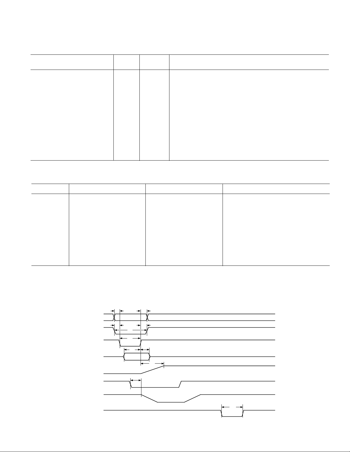
TIMING SPECIFICATIONS
(VCC = +5 V ⴞ 5%; VDD = +15 V ⴞ 10%; VSS = –15 V ⴞ 10%; GND = DUTGND = 0 V)
to production testing.)
Loaded with All 0s and All 1s
(+) = +5 V, V
REF
(–) = –5 V. DAC Latch
REF
Alternately Loaded with 1FFF Hex and 2000 Hex. Not Dependent
on Load Conditions
Input Code to Another Converter
typ All 1s Loaded to DAC. V
(+) = V
REF
(–) = 0 V
REF
Parameter Limit at T
t
1
t
2
t
3
t
4
t
5
t
6
t
7
t
8
t
9
t
10
t
11
NOTES
1
All input signals are specified with tr = tf = 5 ns (10% to 90% of 5 V) and timed from a voltage level of 1.6 V.
2
Rise and fall times should be no longer than 50 ns.
Specifications subject to change without notice.
15 ns min Address to WR Setup Time
0 ns min Address to WR Hold Time
50 ns min CS Pulsewidth Low
50 ns min WR Pulsewidth Low
0 ns min CS to WR Setup Time
0 ns min WR to CS Hold Time
20 ns min Data Setup Time
0 ns min Data Hold Time
31 µs typ Settling Time
300 ns max CLR Pulse Activation Time
50 ns min LDAC Pulsewidth Low
A0, A1, A2
DATA
V
CS
WR
OUT
CLR
MIN, TMAX
t
1
t
5
t
2
t
6
t
3
t
4
t
8
t
7
t
9
t
10
Units Description
V
OUT
LDAC
Figure 1. Timing Diagram
–3–REV. 0
t
11
AD7841
V
DD
V
CC
AD7841
HP5082-2811
V
DD
V
CC
IN4148
ABSOLUTE MAXIMUM RATINGS
(T
= +25°C unless otherwise noted)
A
VCC to GND3 . . . . . . . . . . . . . . . –0.3 V, +7 V or V
1, 2
+ 0.3 V
DD
(Whichever Is Lower)
to GND . . . . . . . . . . . . . . . . . . . . . . . . . . . –0.3 V, +17 V
V
DD
V
to GND . . . . . . . . . . . . . . . . . . . . . . . . . . . . +0.3 V, –17 V
SS
Digital Inputs to GND . . . . . . . . . . . . . . –0.3 V, V
(+) to V
V
REF
V
(+) to GND . . . . . . . . . . . . . . . VSS – 0.3 V, VDD + 0.3 V
REF
V
(–) to GND . . . . . . . . . . . . . . . VSS – 0.3 V, VDD + 0.3 V
REF
DUTGND to GND . . . . . . . . . . . . . V
V
(A–H) to GND . . . . . . . . . . . . VSS – 0.3 V, VDD + 0.3 V
OUT
(–) . . . . . . . . . . . . . . . . . . . . . . –0.3 V, +18 V
REF
– 0.3 V, VDD + 0.3 V
SS
+ 0.3 V
CC
Operating Temperature Range
Industrial (A Version) . . . . . . . . . . . . . . . . –40°C to +85°C
Storage Temperature Range . . . . . . . . . . . . –65°C to +150°C
ORDERING GUIDE
Linearity
Temperature Error DNL Package Package
Model Range (LSBs) (LSBs) Description Option
AD7841AS –40°C to +85°C ±4 –0.9/+2 Plastic Quad Flatpack (MQFP) S-44
AD7841BS –40°C to +85°C ±2 ±1 Plastic Quad Flatpack (MQFP) S-44
Junction Temperature . . . . . . . . . . . . . . . . . . . . . . . . .+150°C
MQFP Package
Power Dissipation . . . . . . . . . . . . . . . . . . (T
Max – T
J
)/θ
A
JA
θJA Thermal Impedance . . . . . . . . . . . . . . . . . . . . . 95°C/W
Lead Temperature, Soldering
Vapor Phase (60 sec) . . . . . . . . . . . . . . . . . . . . . . . .+215°C
Infrared (15 sec) . . . . . . . . . . . . . . . . . . . . . . . . . . .+220°C
ESD . . . . . . . . . . . . . . . . . . . . . . . . . . . . . . . . . . . . . . >4000 V
NOTES
1
Stresses above those listed under Absolute Maximum Ratings may cause perma-
nent damage to the device. This is a stress rating only; functional operation of the
device at these or any other conditions above those indicated in the operational
section of this specification is not implied. Exposure to absolute maximum rating
conditions for extended periods may affect device reliability.
2
Transient currents of up to 100 mA will not cause SCR latch-up.
3
VCC must not exceed VDD by more than 0.3 V. If it is possible for this to happen
during power supply sequencing, the following diode protection scheme will ensure
protection.
DUTGND_AB
V
OUT
V
(–)AB
REF
V
(+)AB
REF
V
DD
V
LDAC
A2
A1
A0
CS
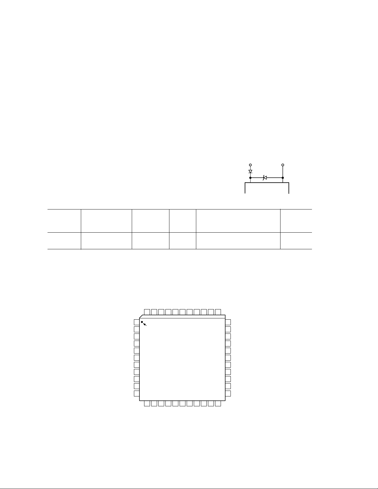
PIN CONFIGURATION
C
OUT
V
DUTGND_CD
CC
V
GND
D
(–)CDEF
OUT
REF
V
V
40 39 3841424344 36 35 3437
AD7841
TOP VIEW
(Not to Scale)
DB1
DB0
B
OUT
V
1
PIN 1
IDENTIFIER
2
A
3
4
5
6
SS
7
8
9
10
11
12 13 14 15 16 17 18 19 20 21 22
WR
(+)CDEF
DD
REF
V
V
DB3
DB2
E
OUT
V
DUTGND_EF
DB5
DB4
F
OUT
V
DB6
G
OUT
V
DB7
33
32
31
30
29
28
27
26
25
24
23
DUTGND_GH
H
V
OUT
V
(–)GH
REF
(+)GH
V
REF
CLR
DB13
DB12
DB11
DB10
DB9
DB8
–4–
REV. 0

PIN FUNCTION DESCRIPTIONS
Pin
No. Mnemonic Description
AD7841
1 DUTGND_AB Device Sense Ground for DACs A and B. V
OUT
A and V
B are referenced to the voltage
OUT
applied to this pin.
2, 32, 34, V
OUT
A..V
H DAC Outputs.
OUT
35, 37, 41,
43, 44
3, 4 V
5, 38 V
6, 29 V
(–)AB, V
REF
DD
SS
(+)AB Reference Inputs for DACs A and B. These reference voltages are referred to GND.
REF
Positive Analog Power Supply; +15 V ± 10% for Special Performance.
Negative Analog Power Supply; –15 V ± 10% for Special Performance.
7 LDAC Load DAC Logic Input (active low). When this logic input is taken low the contents of the
registers are transferred to their respective DAC registers. LDAC can be tied permanently
low enabling the outputs to be updated on the rising edge of WR.
8, 9, 10 A2, A1, A0 Address inputs. A0, A1 and A2 are decoded to select one of the eight input registers for a
data transfer.
11 CS Level-Triggered Chip Select Input (active low). The device is selected when this input is low.
12 WR Level-Triggered Write Input (active low), used in conjunction with CS to write data to the
AD7841 data registers. Data is latched into the selected input register on the rising edge
of WR.
13 V
CC
Logic Power Supply; +5 V ± 5%.
14 GND Ground.
15–28 DB0␣ .␣ .␣ DB12 Parallel Data Inputs. The AD7841 can accept a straight 14-bit parallel word on DB0 to
DB13 where DB13 is the MSB and DB0 is the LSB.
29 CLR Asynchronous Clear Input (level sensitive, active low). When this input is low, all analog
outputs are switched to the externally set potential on the relevant DUTGND pin. The contents of input registers and DAC registers A to H are not affected when the CLR pin is taken
low. When CLR is brought back high, the DAC outputs revert to their original outputs as
determined by the data in their DAC registers.
30, 31 V
33 DUTGND_GH Device Sense Ground for DACs G and H. V
(+)GH, V
REF
(–)GH Reference Inputs for DACs G and H. These reference voltages are referred to GND.
REF
OUT
G and V
H are referenced to the voltage
OUT
applied to this pin.
36 DUTGND_EF Device Sense Ground for DACs E and F. V
OUT
E and V
F are referenced to the voltage
OUT
applied to this pin.
39 V
40 V
42 DUTGND_CD Device Sense Ground for DACs C and D. V
(+)CDEF Reference Inputs for DACs C, D, E and F. These reference voltages are referred to GND.
REF
(–)CDEF Reference Inputs for DACs C, D, E and F. These reference voltages are referred to GND.
REF
OUT
C and V
D are referenced to the voltage
OUT
applied to this pin.
–5–REV. 0

AD7841
TERMINOLOGY
Relative Accuracy
Relative accuracy or endpoint linearity is a measure of the maximum deviation from a straight line passing through the endpoints
of the DAC transfer function. It is measured after adjusting for
zero-scale error and full-scale error and is expressed in Least
Significant Bits.
Differential Nonlinearity
Differential nonlinearity is the difference between the measured
change and the ideal 1 LSB change between any two adjacent
codes. A specified differential nonlinearity of 1 LSB maximum
ensures monotonicity.
DC Crosstalk
Although the common input reference voltage signals are internally buffered, small IR drops in the individual DAC reference
inputs across the die can mean that an update to one channel
can produce a dc output change in one or another of the channel outputs.
The eight DAC outputs are buffered by op amps that share
common V
and VSS power supplies. If the dc load current
DD
changes in one channel (due to an update), this can result in a
further dc change in one or another of the channel outputs. This
effect is most obvious at high load currents and reduces as the
load currents are reduced. With high impedance loads the effect
is virtually impossible to measure.
Output Voltage Settling Time
This is the amount of time it takes for the output to settle to a
specified level for a full-scale input change.
Digital-to-Analog Glitch Impulse
This is the amount of charge injected into the analog output
when the inputs change state. It is specified as the area of the
glitch in nV-secs. It is measured with V
V
(–) = –5 V and the digital inputs toggled between 1FFFH and
REF
(+) = +5 V and
REF
2000H.
Channel-to-Channel Isolation
Channel-to-channel isolation refers to the proportion of input
signal from one DAC’s reference input that appears at the output of another DAC. It is expressed in dBs.
DAC-to-DAC Crosstalk
DAC-to-DAC crosstalk is defined as the glitch impulse that
appears at the output of one converter due to both the digital
change and subsequent analog O/P change at another converter.
It is specified in nV-secs.
Digital Crosstalk
The glitch impulse transferred to the output of one converter
due to a change in digital input code to the other converter is
defined as the digital crosstalk and is specified in nV-secs.
Digital Feedthrough
When the device is not selected, high frequency logic activity on
the device’s digital inputs can be capacitively coupled both
across and through the device to show up as noise on the V
OUT
pins. This noise is digital feedthrough.
DC Output Impedance
This is the effective output source resistance. It is dominated by
package lead resistance.
Full-Scale Error
This is the error in DAC output voltage when all 1s are loaded
into the DAC latch. Ideally the output voltage, with all 1s loaded
into the DAC latch, should be 2 V
Zero-Scale Error
(+) – 1 LSB.
REF
Zero-scale error is the error in the DAC output voltage when all
0s are loaded into the DAC latch. Ideally the output voltage,
with all 0s in the DAC latch should be equal to 2 V
(–). Zero-
REF
scale error is mainly due to offsets in the output amplifier.
Gain Error
Gain Error is defined as (Full-Scale Error) – (Zero-Scale Error).
GENERAL DESCRIPTION
DAC Architecture—General
Each channel consists of a straight 14-bit R-2R voltage-mode
DAC. The full-scale output voltage range is equal to twice the
reference span of V
REF
(+) – V
binary; all 0s produces an output of 2 V
an output of 2 V
(+) – 1 LSB.
REF
(–). The DAC coding is straight
REF
(–); all 1s produces
REF
The analog output voltage of each DAC channel reflects the
contents of its own DAC register. Data is transferred from the
external bus to the input register of each DAC on a per channel
basis.
Bringing the CLR line low switches all the signal outputs, V
to V
H, to the voltage level on the relevant DUTGND pin.
OUT
OUT
A
When the CLR signal is brought back high, the output voltages
from the DACs will reflect the data stored in the relevant DAC
registers.
Data Loading to the AD7841
Data is loaded into the AD7841 in straight parallel 14-bit wide
words.
The DAC output voltages, V
OUT
A – V
H are updated to
OUT
reflect new data in the DAC registers.
The actual input register being written to is determined by the
logic levels present on the device’s address lines, as shown in
Table I.
Table I. Address Line Truth Table
A2 A1 A0 DAC Selected
0 0 0 INPUT REG A (DAC A)
0 0 1 INPUT REG B (DAC B)
0 1 0 INPUT REG C (DAC C)
0 1 1 INPUT REG D (DAC D)
1 0 0 INPUT REG E (DAC E)
1 0 1 INPUT REG F (DAC F)
1 1 0 INPUT REG G (DAC G)
1 1 1 INPUT REG H (DAC H)
–6–
REV. 0

Typical Performance Characteristics–
0 5001000150020002500 3000 350040004500 5000
m
AD7841
2
VDD = +15V
= –15V
V
SS
(+) = +5V
V
REF
1
(–) = –5V
V
REF
= 258C
T
A
0
INL ERROR – LSBs
–1
–2
0 2048
4096 12288 16384
6144 8192 10240 14336
CODE
Figure 2. Typical INL Plot
1
0.5
VDD = +15V
= –15V
V
SS
(+) = +5V
V
REF
(+) = –5V
V
0
REF
DNL ERROR – LSBs
–0.5
–1
–40 100–20020406080
TEMPERATURE – 8C
Figure 5. Typical DNL Error vs.
Temperature
1
0.75
0.5
0.25
0
–0.25
VDD = +15V
DNL ERROR – LSBs
–0.75
–0.5
–1
V
SS
V
REF
V
REF
= 258C
T
A
0 2048
= –15V
(+) = +5V
(–) = –5V
4096 6144 8192
10240 12288 14336 16384
CODE
Figure 3. Typical DNL Plot
4
VDD = +15V
= –15V
V
SS
= +5V
V
REF(+)
2
0
ERROR – LSBs
–2
–4
–40 –20 100
= –5V
V
REF(–)
ZERO-SCALE ERROR
FULL-SCALE ERROR
0 20406080
TEMPERATURE – 8C
Figure 6. Zero-Scale and Full-Scale
Error vs. Temperature
4
VDD = +15V
= –15V
V
SS
(+) = +5V
V
REF
(–) = –5V
V
2
0
INL ERROR – LSBs
–2
–1
REF
–40 –20 1000 20406080
TEMPERATURE – 8C
Figure 4. Typical INL Error vs.
Temperature
6
5
4
DIGITAL INPUTS @
THRESHOLDS
3
– mA
2
CC
I
1
DIGITAL INPUTS @ SUPPLIES
0
–1
–40 100–200 20406080
TEMPERATURE – 8C
VCC = +5V
= +15V
V
DD
V
= –15V
SS
Figure 7. ICC vs. Temperature
0.6
0.5
0.4
0.3
0.2
Volts
0.1
0
–0.1
–0.2
Figure 8. Typical Digital-to-Analog
Glitch Impulse
10.19
10.18
– Volts
OUT
10.17
V
10.16
27 3328 29 30 31 32
SETTLING TIME –
Figure 9. Settling Time (+)
–7–REV. 0
10
VDD = +15V
= –15V
V
SS
= +5V
V
CC
I
8
– mA
SS
/I
DD
I
6
4
s
–40 –20 0 20 40 60
DD
I
SS
TEMPERATURE – °C
80
100
Figure 10. IDD, ISS vs. Temperature

AD7841
Unipolar Configuration
Figure 11 shows the AD7841 in the unipolar binary circuit
configuration. The V
AD586, a +5 V reference. V
(+) input of the DAC is driven by the
REF
(–) is tied to ground. Table II
REF
gives the code table for unipolar operation of the AD7841.
Other suitable references include the REF02, a precision +5 V
reference, and the REF195, a low dropout, micropower precision +5 V reference.
+5V+15V
1mF
2
8
C1
6
AD586
5
R1
4
SIGNAL
GND
*ADDITIONAL PINS OMITTED FOR CLARITY
10kV
V
V
REF
V
REF
DDVCC
(+)
AD7841*
DUTGND
(–)
V
SS
–15V
V
GND
OUT
V
OUT
(0 TO +10V)
SIGNAL
GND
Figure 11. Unipolar +10 V Operation
Offset and gain may be adjusted in Figure 11 as follows: To
adjust offset, disconnect the V
DAC with all 0s and adjust the V
(–) input from 0 V, load the
REF
(–) voltage until V
REF
OUT
= 0 V.
For gain adjustment, the AD7841 should be loaded with all 1s
and R1 adjusted until V
OUT
= 2 V
(+) – 1 LSB = 10 V(16383/
REF
16384) = 9.99939 V.
Many circuits will not require these offset and gain adjustments.
In these circuits R1 can be omitted. Pin 5 of the AD586 may be
left open circuit and Pin 2 (V
(–)) of the AD7841 tied to 0 V.
REF
Table II. Code Table for Unipolar Operation
Binary Number in DAC Register Analog Output
MSB␣␣␣␣␣␣␣␣ LSB (V
11 1111 1111 1111 2 V
10 0000 0000 0000 2 V
01 1111 1111 1111 2 V
00 0000 0000 0001 2 V
)
OUT
(16383/16384) V
REF
(8192/16384) V
REF
(8191/16384) V
REF
(1/16384) V
REF
00 0000 0000 0000 0 V
NOTES
V
= V
(+); V
REF
REF
For V
(+) = +5 V, 1 LSB = +10 V/2
REF
(–) = 0 V for unipolar operation.
REF
14
= +10 V/16384 = 610 µV.
Bipolar Configuration
Figure 12 shows the AD7841 set up for ±10 V operation. The
AD588 provides precision ±5 V tracking outputs that are fed to
the V
(+) and V
REF
(–) inputs of the AD7841. The code table
REF
for bipolar operation of the AD7841 is shown in Table III.
In Figure 12, full-scale and bipolar zero adjustments are provided by varying the gain and balance on the AD588. R2 varies
the gain on the AD588 while R3 adjusts the offset of both the
+5 V and –5 V outputs together with respect to ground.
For bipolar-zero adjustment, the DAC is loaded with
1000␣ .␣ .␣ .␣ 0000 and R3 is adjusted until V
= 0 V. Full scale
OUT
is adjusted by loading the DAC with all 1s and adjusting R2
until V
= 10(8191/8192) V = 9.99878 V.
OUT
When bipolar-zero and full-scale adjustment are not needed, R2
and R3 can be omitted. Pin 12 on the AD588 should be connected to Pin 11 and Pin 5 should be left floating.
V
DDVCC
(+)
AD7841*
DUTGND
(–)
V
SS
–15V
+5V+15V
V
OUT
GND
V
OUT
(–10V TO +10V)
SIGNAL
GND
100kV
R1
39kV
46
7
C1
9
1mF
R2
100kV
5
10
11
12 8 13
R3
2
3
V
REF
1
AD588
14
15
V
REF
16
*ADDITIONAL PINS OMITTED FOR CLARITY
Figure 12. Bipolar ±10 V Operation
Table III. Code Table for Bipolar Operation
Binary Number in DAC
Register Analog Output
MSB LSB (V
11 1111 1111 1111 2[V
10 0000 0000 0001 2[V
10 0000 0000 0000 2[V
01 1111 1111 1111 2[V
00 0000 0000 0001 2[V
00 0000 0000 0000 2[V
NOTES
V
= (V
REF
For V
20 V/16384 = 1.22 mV.
(+) – V
REF
(+) = +5 V, and V
REF
REF
(–)).
(–) = –5 V, V
REF
)
OUT
(–) + V
REF
(–) + V
REF
(–) + V
REF
(–) + V
REF
(–) + V
REF
(–)] V
REF
= 10 V, 1 LSB = 2 V
REF
(16383/16384)] V
REF
(8193/16384)] V
REF
(8192/16384)] V
REF
(8191/16384)] V
REF
(1/16384)] V
REF
REF
V/214 =
CONTROLLED POWER-ON OF THE OUTPUT STAGE
A block diagram of the output stage of the AD7841 is shown in
Figure 13. It is capable of driving a load of 5 kΩ in parallel with
50 pF. G
power on voltage present at V
also used in conjunction with the CLR input to set V
to G6 are transmission gates used to control the
1
. On power up G1 and G2 are
OUT
OUT
to the
user defined voltage present at the DUTGND pin. When CLR
is taken back high, the DAC outputs reflect the data in the DAC
registers.
G
DAC
1
G
G
2
R
DUTGND
G
4
R = 60kV
G
G
6
3
5
14kV
V
OUT
Figure 13. Block Diagram of AD7841 Output Stage
–8–
REV. 0

Power-On with CLR Low
The output stage of the AD7841 has been designed to allow
output stability during power-on. If CLR is kept low during
power-on, then just after power is applied to the AD7841, the
situation is as depicted in Figure 14. G
while G
, G3 and G5 are closed.
2
G
DAC
1
G
2
R
DUTGND
G
4
G
G
Figure 14. Output Stage with VDD < 7 V or VSS > –3 V;
, G4 and G6 are open
1
G
6
3
R
5
14kV
V
OUT
CLR
Low
V
is kept within a few hundred millivolts of DUTGND via
OUT
G
and a 14 kΩ resistor. This thin-film resistor is connected in
5
parallel with the gain resistors of the output amplifier. The
output amplifier is connected as a unity gain buffer via G
the DUTGND voltage is applied to the buffer input via G
, and
3
. The
2
amplifier’s output is thus at the same voltage as the DUTGND
pin. The output stage remains configured as in Figure 14 until
the voltage at V
exceeds 7 V and VSS is more negative than
DD
–3 V. By now the output amplifier has enough headroom to
handle signals at its input and has also had time to settle. The
internal power-on circuitry opens G
G
. This situation is shown in Figure 15. Now the output ampli-
6
fier is configured in its noise gain configuration via G
and G5 and closes G4 and
3
and G6.
4
The DUTGND voltage is still connected to the noninverting
input via G
and this voltage appears at V
2
G
1
DAC
G
3
G
OUT
6
.
V
OUT
AD7841
G
DAC
1
G
G
2
R
DUTGND
G
4
G
Figure 16. Output Stage After
Power-On with CLR High
If CLR is high on the application of power to the device, the
output stages of the AD7841 are configured as in Figure 17
while V
closed and G
is less than 7 V and VSS is more positive than –3 V. G1 is
DD
is open, thereby connecting the output of the
2
DAC to the input of its output amplifier. G
while G
a unity gain buffer. V
through a 14 kΩ resistor until V
and G6 are open, thus connecting the output amplifier as
4
is connected to DUTGND via G
OUT
DD
negative than –3 V.
G
G
1
2
R
DUTGND
G
G
4
G
DAC
Figure 17. Output Stage Powering Up with
While V
< 7 V or VSS > –3 V
DD
When the difference between the supply voltages reaches +10 V,
the internal power-on circuitry opens G
and G6 configuring the output stage as shown in Figure 18.
G
6
3
R
5
14kV
CLR
Is Taken High
and G5 are closed
3
V
OUT
5
exceeds 7 V and VSS is more
G
6
3
R
5
14kV
and G5 and closes G
3
CLR
V
OUT
High
4
G
2
Figure 15.␣ Output Stage with VDD > 7 V and VSS < –3 V;
R
DUTGND
G
4
R
G
5
14kV
CLR
Low
V
has been disconnected from the DUTGND pin by the
OUT
opening of G
, but will track the voltage present at DUTGND
5
via the configuration shown in Figure 15.
When CLR is taken back high, the output stage is configured as
shown in Figure 16. The internal control logic closes G
opens G
. The output amplifier is connected in a noninverting
2
gain-of-two configuration. The voltage that appears on the V
and
1
OUT
pins is determined by the data present in the DAC registers.
–9–REV. 0
G
DAC
1
G
G
2
R
DUTGND
G
4
G
G
6
3
R
5
14kV
Figure 18.␣ Output Stage Powering Up with
When V
> V and VSS < –3 V
DD
CLR
V
OUT
High

AD7841
DUTGND Voltage Range
During power-on, the V
to the relevant DUTGND pins via G
pins of the AD7841 are connected
OUT
and the 14 kΩ thin-film
5
resistor. The DUTGND potential must obey the max ratings at
all times. Thus, the voltage at DUTGND must always be within
the range V
– 0.3 V, V
SS
voltages at the V
OUT
+ 0.3 V. However, in order that the
DD
pins of the AD7841 stay within ±2 V of the
relevant DUTGND potential during power-on, the voltage
applied to DUTGND should also be kept within the range
GND – 2␣ V, GND + 2 V.
Once the AD7841 has powered on and the on-chip amplifiers
have settled, any voltage that is now applied to the DUTGND
pin is subtracted from the DAC output, which has been gained
up by a factor of two. Thus, for specified operation, the maximum voltage that can be applied to the DUTGND pin increases to the maximum allowable 2 V
(+) voltage, and the
REF
minimum voltage that can be applied to DUTGND is the
minimum 2 V
(–) voltage. After the AD7841 has fully
REF
powered on, the outputs can track any DUTGND voltage within
this minimum/maximum range.
Power Supply Sequencing
When operating the AD7841, it is important that ground be
connected at all times to avoid high current states. The recommended power-up sequence is V
followed by VCC. If V
DD/VSS
CC
can exceed VDD on power-up, the diode scheme shown in the
absolute maximum ratings section will ensure protection. The
reference inputs and digital inputs should be powered up last.
Should the references exceed V
on power-up, current
DD/VSS
limiting resistors should be inserted in series with the reference
inputs to limit the current to 20 mA. Logic inputs should not be
applied before V
. Current limiting resistors (470 Ω) in series
CC
with the logic inputs should be inserted if these inputs come up
before V
CC
.
MICROPROCESSOR INTERFACING
Interfacing the AD7841—16-Bit Interface
The AD7841 can be interfaced to a variety of 16-bit microcontrollers or DSP processors. Figure 19 shows the AD7841
interfaced to a generic 16-bit microcontroller/DSP processor.
The lower address lines from the processor are connected to A0,
A1 and A2 on the AD7841 as shown. The upper address lines
are decoded to provide a chip select signal or an LDAC signal
for the AD7841. The fast interface timing of the AD7841 allows
direct interface to a wide variety of microcontrollers and DSPs
as shown in Figure 19.
mCONTROLLER/
DSP PROCESSOR*
D13
DATA
BUS
UPPER BITS OF
ADDRESS BUS
R/W
*ADDITIONAL PINS OMITTED FOR CLARITY
D0
ADDRESS
DECODE
A2
A1
A0
AD7841
D13
D0
CS
LDAC
A2
A1
A0
WR
Figure 19. AD7841 Parallel Interface
APPLICATIONS
Power Supply Bypassing and Grounding
In any circuit where accuracy is important, careful consideration
of the power supply and ground return layout helps to ensure
the rated performance. The printed circuit board on which the
AD7841 is mounted should be designed such that the analog
and digital sections are separated and confined to certain areas
of the board. This facilitates the use of ground planes that can
be easily separated. A minimum etch technique is generally best
for ground planes as it gives the best shielding. Digital and analog ground planes should be joined at only one place. The GND
pin of the AD7841 should be connected to the AGND of the
system. If the AD7841 is in a system where multiple devices
require an AGND-to-DGND connection, the connection should
be made at one point only, a star ground point that should be
established as close as possible to the AD7841.
Digital lines running under the device should be avoided as
these will couple noise onto the die. The analog ground plane
should be allowed to run under the AD7841 to avoid noise
coupling. The power supply lines of the AD7841 should use as
large a trace as possible to provide low impedance paths and
reduce the effects of glitches on the power supply line. Fast
switching signals like clocks should be shielded with digital
ground to avoid radiating noise to other parts of the board and
should never be run near the analog inputs.
Avoid crossover of digital and analog signals. Traces on opposite
sides of the board should run at right angles to each other. This
reduces the effects of feedthrough through the board. A microstrip technique is by far the best but not always possible with a
double sided board. In this technique, the component side of
the board is dedicated to ground plane while signal traces are
placed on the solder side.
The AD7841 should have ample supply bypassing located as
close to the package as possible, ideally right up against the
–10–
REV. 0

AD7841
device. Figure 20 shows the recommended capacitor values of
10 µF in parallel with 0.1 µF on each of the supplies. The 10 µF
capacitors are the tantalum bead type. The 0.1 µF capacitor
should have low Effective Series Resistance (ESR) and Effective
Series Inductance (ESI), such as the common ceramic types,
which provide a low impedance path to ground at high frequencies to handle transient currents due to internal logic switching.
CC
AD7841
V
DD
V
SS
10mF
0.1mF
10mF0.1mF10mF 0.1mF
V
Figure 20. Recommended Decoupling Scheme for AD7841
Automated Test Equipment
The AD7841 is particularly suited for use in an automated test
environment. Figure 21 shows the AD7841 providing the necessary voltages for the pin driver and the window comparator in a
typical ATE pin electronics configuration. AD588s are used to
provide reference voltages for the AD7841. In the configuration
shown, the AD588s are configured so that the voltage at Pin 1 is
5 V greater than the voltage at Pin 9 and the voltage at Pin 15 is
5 V less than the voltage at Pin 9.
+15V –15V
4
6
8
13
10
11
12
1mF
+15V –15V
4
6
8
13
10
11
12
1mF
2
AD588
2
AD588
V
OFFSET
16
3
1
15
14
9
7
16
3
1
15
14
9
7
*ADDITIONAL PINS OMITTED FOR CLARITY
0.1mF
DEVICE
GND
V
(+)AB
REF
(–)AB
V
REF
DUTGND_AB
AD7841*
DUTGND_GH
V
(+)GH
REF
V
(–)GH
REF
GND
V
OUT
V
OUT
V
OUT
V
OUT
COMPARATOR
A
B
G
H
WINDOW
+15V
PIN
DRIVER
–15V
DEVICE
GND
TO TESTER
V
DEVICE
GND
OUT
Figure 21. ATE Application
One of the AD588s is used as a reference for DACs A and B.
These DACs are used to provide high and low levels for the pin
driver. The pin driver may have an associated offset. This can
be nulled by applying an offset voltage to Pin 9 of the AD588.
First, the code 1000␣ .␣ .␣ .␣ 0000 is loaded into the DACA latch
and the pin driver output is set to the DACA output. The
V
driver output and DUTGND. This causes both V
V
TrimDAC is a registered trademark of Analog Devices, Inc.
voltage is adjusted until 0 V appears between the pin
OFFSET
(–) to be offset with respect to GND by an amount equal to
REF
(+) and
REF
–11–REV. 0
V
. However, the output of the pin driver will vary from
OFFSET
–10 V to +10 V with respect to DUTGND as the DAC input
code varies from 000␣ .␣ .␣ .␣ 000 to 111␣ .␣ .␣ .␣ 111. The V
OFFSET
voltage is also applied to the DUTGND pins. When a clear is
performed on the AD7841, the output of the pin driver will be
0 V with respect to DUTGND.
The other AD588 is used to provide a reference voltage for
DACs G and H. These provide the reference voltages for the
window comparator shown in the diagram. Note that Pin 9 of
this AD588 is connected to Device GND. This causes V
and V
(–)GH to be referenced to Device GND. As DAC G
REF
REF
(+)GH
and DAC H input codes vary from 000␣ .␣ .␣ .␣ 000 to 111␣ .␣ .␣ .␣ 111,
V
G and V
OUT
H vary from –10 V to +10 V with respect to
OUT
Device GND. Device GND is also connected to DUTGND.
When the AD7841 is cleared, V
OUT
G and V
H are cleared to
OUT
0 V with respect to Device GND.
Programmable Reference Generation for the AD7841 in an
ATE Application
The AD7841 is particularly suited for use in an automated test
environment. The reference input for the AD7841 octal 14-bit
DAC requires three differential references for the eight DACs.
Programmable references may be a requirement in some ATE
applications as the offset and gain errors at the output of a DAC
can be adjusted by varying the voltages on the reference pins of
the DAC. To trim offset errors, the DAC is loaded with the
digital code 000␣ .␣ .␣ .␣ 000 and the voltage on the V
(–) pin is
REF
adjusted until the desired negative output voltage is obtained.
To trim out gain errors, first the offset error is trimmed. Then
the DAC is loaded with the code 111␣ .␣ .␣ .␣ 111 and the voltage
on the V
(+) pin is adjusted until the desired full-scale voltage
REF
minus one LSB is obtained.
It is not uncommon in ATE design, to have other circuitry at
the output of the AD7841 that can have offset and gain errors of
up to say ±300 mV. These offset and gain errors can be easily
removed by adjusting the reference voltages of the AD7841.
The AD7841 uses nominal reference values of ±5 V to achieve
an output span of ±10 V. Since the AD7841 has a gain of two
from the reference inputs to the DAC output, adjusting the
reference voltages by ±150 mV will adjust the DAC offset and
gain by ±300 mV.
There are a number of suitable 8- and 10-bit DACs available
that would be suitable to drive the reference inputs of the
AD7841, such as the AD7804, a quad 10-bit digital-to-analog
converter with serial load capabilities. The voltage output from
this DAC is in the form of V
BIAS
±
V
and rail-to-rail opera-
SWING
tion is achievable. The voltage reference for this DAC can be
internally generated or provided externally. This DAC also
contains an 8-bit SUB DAC which can be used to shift the
complete transfer function of each DAC around the V
BIAS
point.
This can be used as a fine trim on the output voltage. In this
application two AD7804s are required to provide programmable
reference capability for all eight DACs. One AD7804 is used to
drive the V
V
(–) pins.
REF
Another suitable DAC for providing programmable reference
capability is the AD8803. This is an octal 8-bit trimDAC
(+) pins and the second package used to drive the
REF
®
and
provides independent control of both the top and bottom ends
of the trimDAC. This is helpful in maximizing the resolution of
devices with a limited allowable voltage control range.

AD7841
The AD8803 has an output voltage range of GND to VDD (0 V
to +5 V). To trim the V
on the AD8803 DAC can be set using the V
(+) input, the appropriate trim range
REF
REFL
and V
REFH
pins
allowing 8 bits of resolution between the two points. This will
allow the V
To trim the V
(+) pin to be adjusted to remove gain errors.
REF
(–) voltage, some method of providing a trim
REF
voltage in the required negative voltage range is required. Neither the AD7804 or the AD8803 can provide this range in normal operation as their output range is 0 V to +5 V. There are
two methods of producing this negative voltage. One method is
ADDR BUS
+5V
ADDR
SDATA
SCLK
CONTROLLER
DECODER
LOGIC LEVEL
SHIFT
FSIN/CS
D IN
SCLK
FSIN/CS
D IN
SCLK
8/10-BIT
DAC
8/10-BIT
DAC
V
GND
V
GND
to provide a positive output voltage and then to level shift that
analog voltage to the required negative range. Alternatively
these DACs can be operated with supplies of 0 V and –5 V, with
the V
pin connected to 0 V and the GND pin connected to
DD
–5 V. Now these can be used to provide the negative reference
voltages for the V
(–) inputs on the AD7841. However, the
REF
digital signals driving the DACs need to be level-shifted from
the 0 V to +5 V range to the –5 V to 0 V range. Figure 22 shows
a typical application circuit to provide programmable reference
capabilities for the AD7841.
DD
0V TO +5V
DD
0V TO 25V
V
REF
V
REF
A0, A1, A2
(+)AB
AD7841*
(2)AB
V
A
V
OUT
V
B
OUT
A
OUT
V
B
OUT
C3402–2–4/99
DATA BUS
25V
DATA BUS
*ADDITIONAL PINS OMITTED FOR CLARITY
GND
Figure 22. Programmable Reference Generation for the AD7841
OUTLINE DIMENSIONS
Dimensions shown in inches and (mm).
44-Lead MQFP (S-44)
0.548 (13.925)
34
33
0.546 (13.875)
0.398 (10.11)
0.390 (9.91)
TOP VIEW
(PINS DOWN)
23
22
0.037 (0.94)
0.025 (0.64)
SEATING
PLANE
0.096 (2.44)
MAX
8°
0.8°
PRINTED IN U.S.A.
0.040 (1.02)
0.032 (0.81)
0.083 (2.11)
0.077 (1.96)
0.040 (1.02)
0.032 (0.81)
44
–12–
1
0.033 (0.84)
0.029 (0.74)
12
11
0.016 (0.41)
0.012 (0.30)
REV. 0
 Loading...