

LC2MOS
a
FEATURES
Complete 14-Bit Voltage Output DAC
Parallel and Serial Interface Capability
80 dB Signal-to-Noise Ratio
Interfaces to High Speed DSP Processors
e.g., ADSP-2100, TMS32010, TMS32020
45 ns min
Low Power – 70 mW typ.
Operates from 65 V Supplies
GENERAL DESCRIPTION
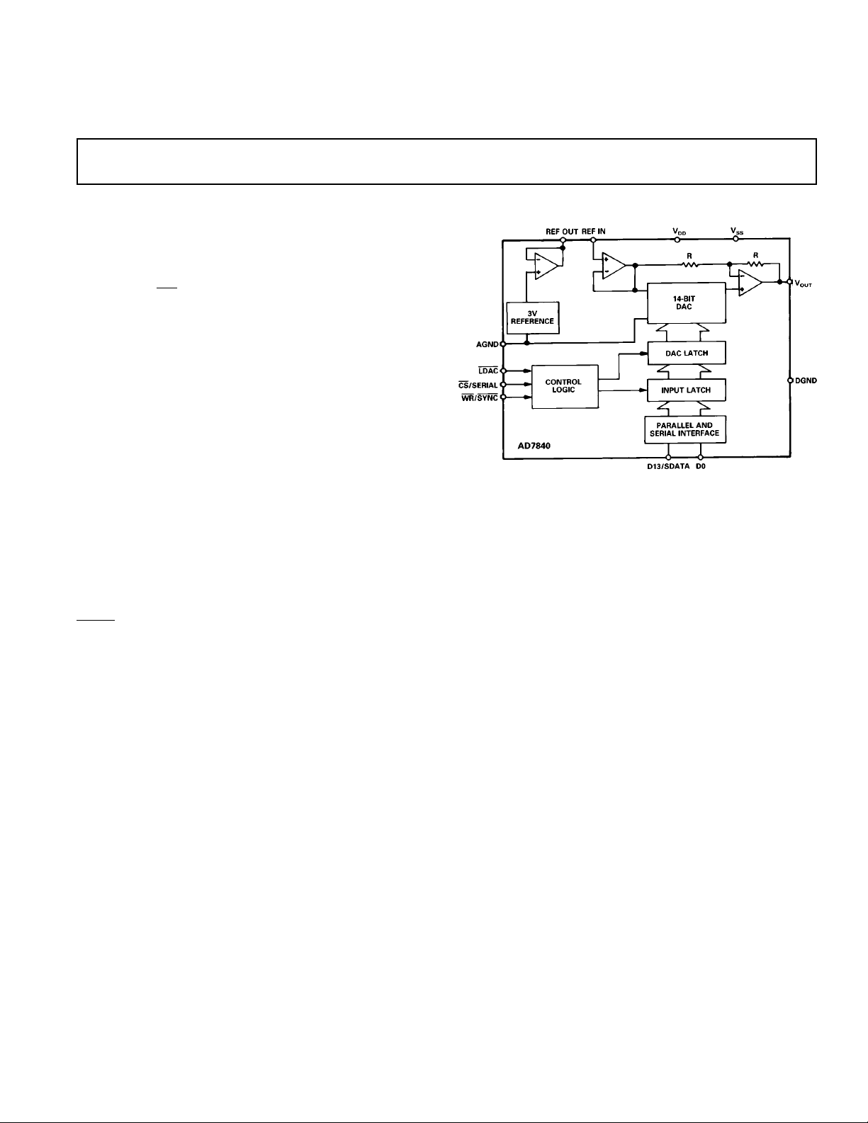
The AD7840 is a fast, complete 14-bit voltage output D/A converter. It consists of a 14-bit DAC, 3 V buried Zener reference,
DAC output amplifier and high speed control logic.
The part features double-buffered interface logic with a 14-bit
input latch and 14-bit DAC latch. Data is loaded to the input
latch in either of two modes, parallel or serial. This data is then
transferred to the DAC latch under control of an asynchronous
LDAC signal. A fast data setup time of 21 ns allows direct
parallel interfacing to digital signal processors and high speed
16-bit microprocessors. In the serial mode, the maximum serial
data clock rate can be as high as 6 MHz.
The analog output from the AD7840 provides a bipolar output
range of ±3 V. The AD7840 is fully specified for dynamic performance parameters such as signal-to-noise ratio and harmonic
distortion as well as for traditional dc specifications. Full power
output signals up to 20 kHz can be created.
The AD7840 is fabricated in linear compatible CMOS
2
(LC
MOS), an advanced, mixed technology process that combines precision bipolar circuits with low power CMOS logic.
The part is available in a 24-pin plastic and hermetic
dual-in-line package (DIP) and is also packaged in a 28-terminal plastic leaded chip carrier (PLCC).
WR Pulse Width
Complete 14-Bit DAC
AD7840
FUNCTIONAL BLOCK DIAGRAM
PRODUCT HIGHLIGHTS
1. Complete 14-Bit D/A Function
The AD7840 provides the complete function for creating ac
signals and dc voltages to 14-bit accuracy. The part features
an on-chip reference, an output buffer amplifier and 14-bit
D/A converter.
2. Dynamic Specifications for DSP Users
In addition to traditional dc specifications, the AD7840 is
specified for ac parameters including signal-to-noise ratio and
harmonic distortion. These parameters along with important
timing parameters are tested on every device.
3. Fast, Versatile Microprocessor Interface
The AD7840 is capable of 14-bit parallel and serial interfacing. In the parallel mode, data setup times of 21 ns and write
pulse widths of 45 ns make the AD7840 compatible with
modern 16-bit microprocessors and digital signal processors.
In the serial mode, the part features a high data transfer rate
of 6 MHz.
REV. B
Information furnished by Analog Devices is believed to be accurate and
reliable. However, no responsibility is assumed by Analog Devices for its
use, nor for any infringements of patents or other rights of third parties
which may result from its use. No license is granted by implication or
otherwise under any patent or patent rights of Analog Devices.
One Technology Way, P.O. Box 9106, Norwood, MA 02062-9106, U.S.A.
Tel: 617/329-4700 Fax: 617/326-8703

(VDD = +5 V 6 5%, VSS = –5 V 6 5%, AGND = DGND = O V, REF IN = +3 V, RL = 2 kV,
AD7840–SPECIFICA TIONS
Parameter J, A1K, B1S
DYNAMIC PERFORMANCE
Signal to Noise Ratio3 (SNR) 76 78 76 dB min V
2
CL = 100 pF. All specifications T
1
Units Test Conditions/Comments
to T
MIN
OUT
unless othewise noted.)
MAX
= 1 kHz Sine Wave, f
SAMPLE
Typically 82 dB at +25°C for 0 < V
Total Harmonic Distortion (THD) –78 –80 –78 dB max V
= 1 kHz Sine Wave, f
OUT
SAMPLE
Typically –84 dB at +25°C for 0 < V
Peak Harmonic or Spurious Noise –78 –80 –78 dB max V
= 1 kHz Sine Wave, f
OUT
SAMPLE
Typically –84 dB at +25°C for 0 < V
DC ACCURACY
Resolution 14 14 14 Bits
Integral Nonlinearity ±2 ±1 ±2 LSB max
Differential Nonlinearity ± 0.9 ± 0.9 ± 0.9 LSB max Guaranteed Monotonic
Bipolar Zero Error ±10 ±10 ±10 LSB max
Positive Full Scale Error
Negative Full Scale Error
REFERENCE OUTPUT
5
5
6
±10 ±10 ±10 LSB max
±10 ±10 ±10 LSB max
REF OUT @ +25°C 2.99 2.99 2.99 V min
3.01 3.01 3.01 V max
REF OUT TC ±60 ±60 ±60 ppm/°C max
Reference Load Change
(∆REF OUT vs. ∆I) –1 –1 –1 mV max Reference Load Current Change (0–500 µA)
= 100 kHz
< 20 kHz
OUT
= 100 kHz
< 20 kHz
OUT
= 100 kHz
< 20 kHz
OUT
4
4
4
REFERENCE INPUT
Reference Input Range 2.85 2.85 2.85 V min 3 V ± 5%
3.15 3.15 3.15 V max
Input Current 50 50 50 µA max
LOGIC INPUTS
Input High Voltage, V
Input Low Voltage, V
Input Current, I
Input Current (CS Input Only) ±10 ±10 ±10 µA max VIN =VSS to V
Input Capacitance, C
INH
INL
IN
7
IN
2.4 2.4 2.4 V min VDD = 5 V ± 5%
0.8 0.8 0.8 V max VDD = 5 V ± 5%
±10 ±10 ±10 µA max VIN = 0 V to V
DD
DD
10 10 10 pF max
ANALOG OUTPUT
Output Voltage Range ±3 ±3 ±3 V nom
DC Output Impedance 0.1 0.1 0.1 Ω typ
Short-Circuit Current 20 20 20 mA typ
AC CHARACTERISTICS
7
Voltage Output Settling Time Settling Time to within ± 1/2 LSB of Final Value
Positive Full-Scale Change 4 4 4 µs max Typically 2 µs
Negative Full-Scale Change 4 4 4 µs max Typically 2.5 µs
Digital-to-Analog Glitch Impulse 10 10 10 nV secs typ
Digital Feedthrough 2 2 2 nV secs typ
POWER REQUIREMENTS
V
DD
V
SS
I
DD
I
SS
+5 +5 +5 V nom ±5% for Specified Performance
–5 –5 –5 V nom ±5% for Specified Performance
14 14 15 mA max Output Unloaded, SCLK = +5 V. Typically 10 mA
6 6 7 mA max Output Unloaded, SCLK = +5 V. Typically 4 mA
Power Dissipation 100 100 110 mW max Typically 70 mW
NOTES
1
Temperature ranges are as follows: J, K Versions, 0°C to +70 °C; A, B Versions, –25 °C to +85 °C; S Version, –55° C to +125° C.
2
V
(pk-pk) = ±3 V
OUT
3
SNR calculation includes distortion and noise components.
4
Using external sample-and-hold (see Testing the AD7840).
5
Measured with respect to REF IN and includes bipolar offset error.
6
For capacitive loads greater than 50 pF, a series resistor is required (see Internal Reference section).
7
Sample tested @ +25°C to ensure compliance.
Specifications subject to change without notice.
–2–
REV. B
AD7840
WARNING!
ESD SENSITIVE DEVICE
, T
1, 2
(VDD = +5 V 6 5%, VSS = –5 V 6 5%, AGND = DGND = 0 V.)
MAX
Limit at T
MIN
, T
MAX
TIMING CHARACTERISTICS
Limit at T
MIN
Parameter (J, K, A, B Versions) (S Version) Units Conditions/Comments
t
1
t
2
t
3
t
4
t
5
t
6
t
7
3
t
8
t
9
t
10
t
11
NOTES
1
Timing specifications in bold print are 100% production tested. All other times are sample tested at +25°C to ensure compliance. All input signals are specified with
tr = tf = 5 ns (10% to 90% of 5 V) and timed from a voltage level of 1.6 V.
2
See Figures 6 and 8.
3
SCLK mark/space ratio is 40/60 to 60/40.
Specifications subject to change without notice.
ABSOLUTE MAXIMUM RATINGS*
VDD to AGND . . . . . . . . . . . . . . . . . . . . . . . . . –0.3 V to +7 V
V
to AGND . . . . . . . . . . . . . . . . . . . . . . . . . +0.3 V to –7 V
SS
AGND to DGND . . . . . . . . . . . . . . . . –0.3 V to V
V
to AGND . . . . . . . . . . . . . . . . . . . . . . . . . . . VSS to V
OUT
REF OUT to AGND . . . . . . . . . . . . . . . . . . . . . . . 0 V to V
REF IN to AGND . . . . . . . . . . . . . . . . –0.3 V to VDD + 0.3 V
Digital Inputs to DGND . . . . . . . . . . . –0.3 V to V
Operating Temperature Range
Commercial (J, K Versions) . . . . . . . . . . . . . .0°C to +70°C
Industrial (A, B Versions) . . . . . . . . . . . . . . –25°C to +85°C
Extended (S Version) . . . . . . . . . . . . . . . . –55°C to +125°C
Storage Temperature Range . . . . . . . . . . . . –65°C to +150°C
Lead Temperature (Soldering, 10 sec) . . . . . . . . . . . . +300°C
Power Dissipation (Any Package) to +75°C . . . . . . . . 450 mW
Derates above +75°C by . . . . . . . . . . . . . . . . . . . . 10 mW/°C
*Stresses above those listed under “Absolute Maximum Ratings” may cause
permanent damage to the device. This is a stress rating only and functional
operation of the device at these or any other conditions above those listed in the
operational sections of this specification is not implied. Exposure to absolute
maximum rating conditions for extended periods may affect device reliability.
0 0 ns min CS to WR Setup Time
0 0 ns min CS to WR Hold Time
45 50 ns min WR Pulse Width
21 28 ns min Data Valid to WR Setup Time
10 15 ns min Data Valid to WR Hold Time
40 40 ns min LDAC Pulse Width
50 50 ns min SYNC to SCLK Falling Edge
150 200 ns min SCLK Cycle Time
30 40 ns min Data Valid to SCLK Setup Time
75 100 ns min Data Valid to SCLK Hold Time
75 100 ns min SYNC to SCLK Hold Time
ORDERING GUIDE
Integral
+ 0.3 V
DD
DD
DD
1
Model
AD7840JN 0°C to +70°C 78 min ±2 max N-24
Temperature SNR Nonlinearity Package
Range (dB) (LSB) Option
2
AD7840KN 0°C to +70°C 80 min ±1 max N-24
+ 0.3 V
DD
AD7840JP 0°C to +70°C 78 min ±2 max P-28A
AD7840KP 0°C to +70°C 80 min ±1 max P-28A
AD7840AQ –25°C to +85°C 78 min ± 2 max Q-24
AD7840ARS –25°C to +85°C 78 min ±2 max RS-24
AD7840BQ –25°C to +85°C 80 min ±1 max Q-24
AD7840SQ3–55°C to +125°C 78 min ± 2 max Q-2
NOTES
1
To order MIL-STD-883, Class B processed parts, add /883B to part number.
Contact your local sales office for military data sheet and availability.
2
N = Plastic DIP; P = Plastic Leaded Chip Carrier; Q = Cerdip.
3
This grade will be available to /883B processing only.
4
CAUTION
ESD (electrostatic discharge) sensitive device. Electrostatic charges as high as 4000 V readily
accumulate on the human body and test equipment and can discharge without detection.
Although the AD7840 features proprietary ESD protection circuitry, permanent damage may
occur on devices subjected to high energy electrostatic discharges. Therefore, proper ESD
precautions are recommended to avoid performance degradation or loss of functionality.
REV. B
–3–
AD7840
DIP
Pin Pin
No. Mnemonic Function
PIN FUNCTION DESCRIPTION
1
CS/SERIAL Chip Select/Serial Input. When driven with normal logic levels, it is an active low logic input which is used
in conjunction with
nently low, an R, C is required for correct power-up (see
WR to load parallel data to the input latch. For applications where CS is perma-
LDAC input). If this input is tied to VSS, it de-
fines the AD7840 for serial mode operation.
2 WR/SYNC Write/Frame Synchronization Input. In the parallel data mode, it is used in conjunction with CS to load
parallel data. In the serial mode of operation, this pin functions as a Frame Synchronization pulse with serial data expected after the falling edge of this signal.
3 D13/SDATA Data Bit 13(MSB)/Serial Data. When parallel data is selected, this pin is the D13 input. In serial mode,
SDATA is the serial data input which is used in conjunction with
SYNC and SCLK to transfer serial data
to the AD7840 input latch.
4 D12/SCLK Data Bit 12/Serial Clock. When parallel data is selected, this pin is the D12 input. In the serial mode, it is
the serial clock input. Serial data bits are latched on the falling edge of SCLK when
SYNC is low.
5 D11/FORMAT Data Bit 11/Data Format. When parallel data is selected, this pin is the D11 input. In serial mode, a Logic
1 on this input indicates that the MSB is the first valid bit in the serial data stream. A Logic 0 indicates
that the LSB is the first valid bit (see Table I).
6 D10/JUSTIFY Data Bit 10/Data Justification. When parallel data is selected, this pin is the D10 input. In serial mode,
this input controls the serial data justification (see Table I).
7–11 D9–D5 Data Bit 9 to Data Bit 5. Parallel data inputs.
12 DGND Digital Ground. Ground reference for digital circuitry.
13–16 D4–D1 Data Bit 4 to Data Bit 1. Parallel data inputs.
17 D0 Data Bit 0 (LSB). Parallel data input.
18 V
DD
Positive Supply, +5 V ± 5%.
19 AGND Analog Ground. Ground reference for DAC, reference and output buffer amplifier.
20 V
OUT
Analog Output Voltage. This is the buffer amplifier output voltage. Bipolar output range (±3 V with REF
IN = +3 V).
21 V
SS
Negative Supply Voltage, –5 V ± 5%.
22 REF OUT Voltage Reference Output. The internal 3 V analog reference is provided at this pin. To operate the
AD7840 with internal reference, REF OUT should be connected to REF IN. The external load capability
of the reference is 500 µA.
23 REF IN Voltage Reference Input. The reference voltage for the DAC is applied to this pin. It is internally buffered
before being applied to the DAC. The nominal reference voltage for correct operation of the AD7840 is
3 V.
24
LDAC Load DAC. Logic Input. A new word is loaded into the DAC latch from the input latch on the falling
edge of this signal (see Interface Logic Information section). The AD7840 should be powered-up with
LDAC high. For applications where LDAC is permanently low, an R, C is required for correct power-up
(see Figure 19).
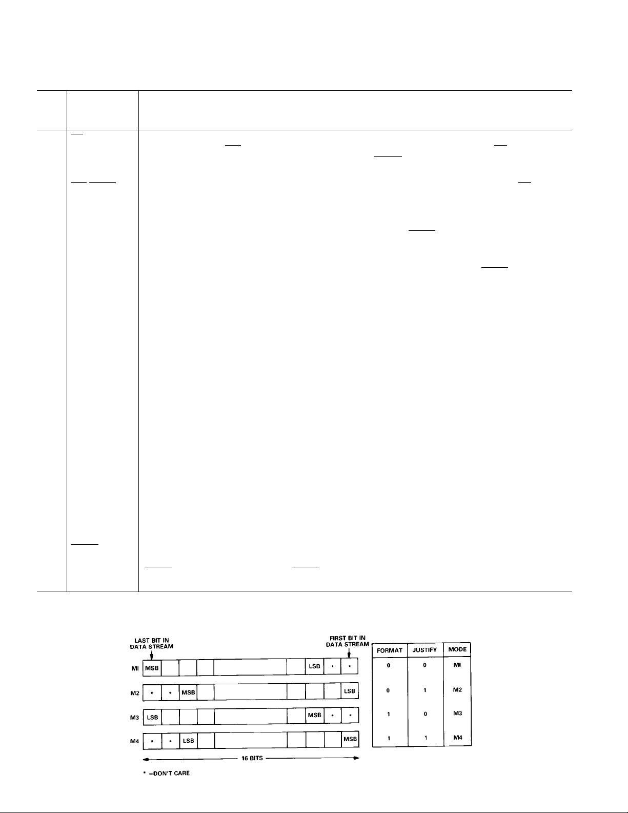
Table I. Serial Data Modes
–4–
REV. B
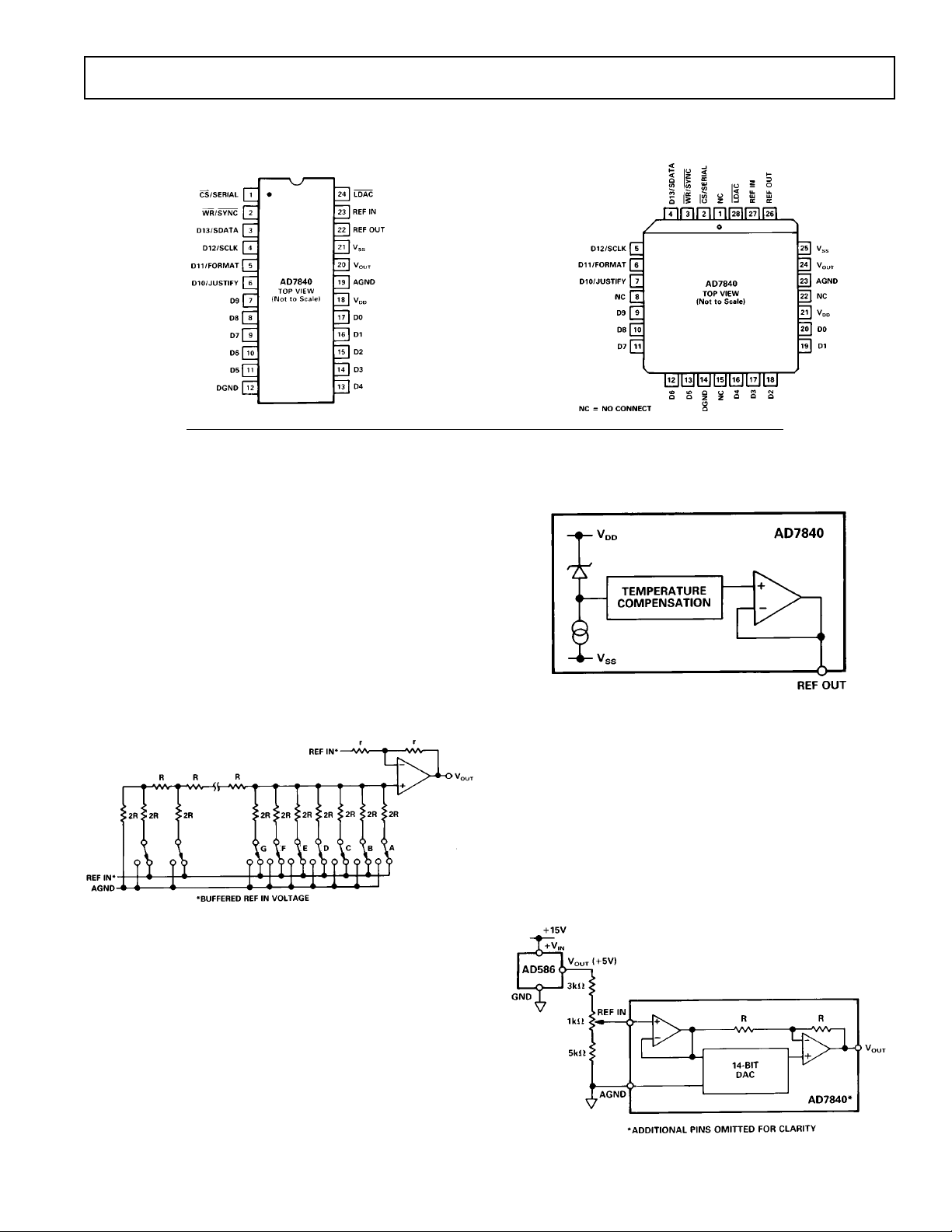
PIN CONFIGURATIONS
DIP/SSOP PLCC
AD7840
D/A SECTION
The AD7840 contains a 14-bit voltage mode D/A converter
consisting of highly stable thin film resistors and high speed
NMOS single-pole, double-throw switches. The simplified circuit diagram for the DAC section is shown in Figure 1. The
three MSBs of the data word are decoded to drive the seven
switches A–G. The 11 LSBs switch an 11-bit R-2R ladder structure. The output voltage from this converter has the same polarity as the reference voltage, REF IN.
The REF IN voltage is internally buffered by a unity gain amplifier before being applied to the D/A converter and the bipolar
bias circuitry. The D/A converter is configured and sealed for a
3 V reference and the device is tested with 3 V applied to REF
IN. Operating the AD7840 at reference voltages outside the
±5% tolerance range may result in degraded performance from
the part.
Figure 1. DAC Ladder Structure
for external use, it should he decoupled to AGND with a 200 Ω
resistor in series with a parallel combination of a 10 µF tantalum
capacitor and a 0.1 µF ceramic capacitor.
Figure 2. Internal Reference
EXTERNAL REFERENCE
In some applications, the user may require a system reference or
some other external reference to drive the AD7840 reference input. Figure 3 shows how the AD586 5 V reference can be conditioned to provide the 3 V reference required by the AD7840
REF IN. An alternate source of reference voltage for the
AD7840 in systems which use both a DAC and an ADC is to
use the REF OUT voltage of ADCs such as the AD7870 and
AD7871. A circuit showing this arrangement is shown in
Figure 20.
INTERNAL REFERENCE
The AD7840 has an on-chip temperature compensated buried
Zener reference (see Figure 2) which is factory trimmed to 3 V
±10 mV. The reference voltage is provided at the REF OUT
pin. This reference can be used to provide both the reference
voltage for the D/A converter and the bipolar bias circuitry. This
is achieved by connecting the REF OUT pin to the REF IN pin
of the device.
The reference voltage can also be used as a reference for other
components and is capable of providing up to 500 µA to an ex-
ternal load. The maximum recommended capacitance on REF
OUT for normal operation is 50 pF. If the reference is required
REV. B
–5–
Figure 3. AD586 Driving AD7840 REF IN

AD7840
OP AMP SECTION
The output from the voltage mode DAC is buffered by a
noninverting amplifier. Internal scaling resistors on the AD7840
configure an output voltage range of ± 3 V for an input reference
voltage of +3 V. The arrangement of these resistors around the
output op amp is as shown in Figure 1. The buffer amplifier is
capable of developing ±3 V across a 2 kΩ and 100 pF load to
ground and can produce 6 V peak-to-peak sine wave signals to a
frequency of 20 kHz. The output is updated on the falling edge
of the
LDAC input. The amplifier settles to within 1/2 LSB of
its final value in typically less than 2.5 µs.
The small signal (200 mV p-p) bandwidth of the output buffer
amplifier is typically 1 MHz. The output noise from the amplifier is low with a figure of 30 nV/√
Hz at a frequency of 1 kHz.
The broadband noise from the amplifier exhibits a typical peakto-peak figure of 150 µV for a 1 MHz output bandwidth. Figure
4 shows a typical plot of noise spectral density versus frequency
for the output buffer amplifier and for the on-chip reference.
Figure 4. Noise Spectral Density vs. Frequency
TRANSFER FUNCTION
The basic circuit configuration for the AD7840 is shown in Figure 5. Table II shows the ideal input code to output voltage relationship for this configuration. Input coding to the DAC is 2s
complement with 1 LSB = FS/16,384 = 6 V/16,384 = 366 µV.
Table II. Ideal Input/Output Code Table
DAC Latch Contents
MSB LSB Analog Output, V
OUT
*
0 1 1 1 1 1 1 1 1 1 1 1 1 1 +2.999634 V
0 1 1 1 1 1 1 1 1 1 1 1 1 0 +2.999268 V
0 0 0 0 0 0 0 0 0 0 0 0 0 1 +0.000366 V
0 0 0 0 0 0 0 0 0 0 0 0 0 0 0 V
1 1 1 1 1 1 1 1 1 1 1 1 1 1 –0.000366 V
1 0 0 0 0 0 0 0 0 0 0 0 0 1 –2.999634 V
1 0 0 0 0 0 0 0 0 0 0 0 0 0 –3 V
*Assuming REF IN = +3 V.
The output voltage can be expressed in terms of the input code,
N, using the following expression:
OUT
=
2×N × REFIN
16384
−8192 ≤ N ≤+8191
V
INTERFACE LOGIC INFORMATION
The AD7840 contains two 14-bit latches, an input latch and a
DAC latch. Data can be loaded to the input latch in one of two
basic interface formats. The first is a parallel 14-bit wide data
word; the second is a serial interface where 16 bits of data are
serially clocked into the input latch. In the parallel mode,
and
WR control the loading of data. When the serial data format
is selected, data is loaded using the SCLK,
SYNC and SDATA
CS
serial inputs. Data is transferred from the input latch to the
DAC latch under control of the
LDAC signal. Only the data in
the DAC latch determines the analog output of the AD7840.
Parallel Data Format
Table III shows the truth table for AD7840 parallel mode operation. The AD7840 normally operates with a parallel input
data format. In this case, all 14 bits of data (appearing on data
inputs D13 (MSB) through D0 (LSB)) are loaded to the
AD7840 input latch at the same time.
CS and WR control the
loading of this data. These control signals are level-triggered;
therefore, the input latch can be made transparent by holding
both signals at a logic low level. Input data is latched into the input latch on the rising edge of
CS or WR.
The DAC latch is also level triggered. The DAC output is normally updated on the falling edge of the
LDAC signal. However,
both latches cannot become transparent at the same time.
Therefore, if
lows; with
transparent. When
LDAC is hardwired low, the part operates as fol-
LDAC low and CS and WR high, the DAC latch is
CS and WR go low (with LDAC still low),
the input latch becomes transparent but the DAC latch is disabled. When
CS or WR return high, the input latch is locked
out and the DAC latch becomes transparent again and the DAC
output is updated. The write cycle timing diagram for parallel
data is shown in Figure 6. Figure 7 shows the simplified parallel
input control logic for the AD7840.
Figure 5. AD7840 Basic Connection Diagram
–6–
REV. B

AD7840
Table III. Parallel Mode Truth Table
CS WR LDAC Function
HX H
XH H
L L H Input Latch Transparent
HH L
H X L DAC Latch Transparent
X H L Analog Output Updated
ff
L
g
g
L
X = Don’t Care
L Input Latch Transparent
L
Figure 6. Parallel Mode Timing Diagram
Both Latches Latched
}
Input Latch Latched
}
DAC Latch Data Transfer Inhibited
Input Latch Is Latched
}
DAC Latch Data Transfer Occurs
Serial Data Format
The serial data format is selected for the AD7840 by connecting
the
CS/SERIAL line to –5 V. In this case, the WR/SYNC,
D13/SDATA, D12/SCLK, D11/FORMAT and D10/JUSTIFY
pins all assume their serial functions. The unused parallel inputs
should not be left unconnected to avoid noise pickup. Serial
data is loaded to the input latch under control of SCLK,
and SDATA. The AD7840 expects a 16-bit stream of serial data
on its SDATA input. Serial data must be valid on the falling
edge of SCLK. The
zation signal which tells the AD7840 that valid serial data will
be available for the next 16 falling edges of SCLK. Figure 8
shows the timing diagram for serial data format.
SYNC input provides the frame synchroni-
SYNC
Figure 7. AD7840 Simplified Parallel Input Control Logic
Figure 8. Serial Mode Timing Diagram
Although 16 bits of data are clocked into the AD7840, only 14
bits go into the input latch. Therefore, two bits in the stream are
don’t cares since their value does not affect the input latch data.
The order and position in which the AD7840 accepts the 14 bits
of input data depends upon the FORMAT and JUSTIFY inputs. There are four different input data modes which can be
chosen (see Table I in the Pin Function Description section).
The first mode (M1) assumes that the first two bits of the input
data stream are don’t cares, the third bit is the LSB and the last
(or 16th bit) is the MSB. This mode is chosen by tying both the
FORMAT and JUSTIFY pins to a logic 0. The second mode
(M2; FORMAT = 0, JUSTIFY = 1) assumes that the first bit in
the data stream is the LSB, the fourteenth bit is the MSB and
the last two bits are don’t cares. The third mode (M3;
FORMAT= 1, JUSTIFY 0) assumes that the first two bits in
the stream are again don’t cares, the third bit is now the MSB
and the sixteenth bit is the LSB. The final mode (M4; FORMAT = 1, JUSTIFY= 1) assumes that the first bit is the MSB,
the fourteenth bit is the LSB and the last two bits of the stream
are don’t cares.
REV. B
–7–

AD7840
As in the parallel mode, the LDAC signal controls the loading
of data to the DAC latch. Normally, data is loaded to the DAC
latch on the falling edge of
LDAC. However, if LDAC is held
low, then serial data is loaded to the DAC latch on the sixteenth
falling edge of SCLK. If
LDAC goes low during the transfer of
serial data to the input latch, no DAC latch update takes place
on the falling edge of
LDAC. If LDAC stays low until the serial
transfer is completed, then the update takes place on the sixteenth falling edge of SCLK. If
LDAC returns high before the
serial data transfer is completed, no DAC latch update takes
place. Figure 9 shows the simplified serial input control logic for
the AD7840.
Figure 9. AD7840 Simplified Serial Input Control Logic
AD7840 DYNAMIC SPECIFICATIONS
The AD7840 is specified and 100% tested for dynamic performance specifications as well as traditional dc specifications such
as integral and differential nonlinearity. These ac specifications
are required for the signal processing applications such as
speech synthesis, servo control and high speed modems. These
applications require information on the DAC’s effect on the
spectral content of the signal it is creating. Hence, the parameters for which the AD7840 is specified include signal-to-noise
ratio, harmonic distortion and peak harmonics. These terms are
discussed in more detail in the following sections.
Signal-to-Noise Ratio (SNR)
SNR is the measured signal-to-noise ratio at the output of the
DAC. The signal is the rms magnitude of the fundamental.
Noise is the rms sum of all the nonfundamental signals up to
half the sampling frequency (fs/2) excluding dc. SNR is dependent upon the number of quantization levels used in the digitization process; the more levels, the smaller the quantization
noise. The theoretical signal to noise ratio for a sine wave output is given by
SNR = (6.02N + 1.76) dB (1)
where N is the number of bits. Thus for an ideal 14-bit converter, SNR = 86 dB.
Figure 10 shows a typical 2048 point Fast Fourier Transform
(FFT) plot of the AD7840KN with an output frequency of
1 kHz and an update rate of 100 kHz. The SNR obtained from
this graph is 81.8 dB. It should be noted that the harmonics are
taken into account when calculating the SNR.
Figure 10. AD7840 FFT Plot
Effective Number of Bits
The formula given in (1) relates the SNR to the number of bits.
Rewriting the formula, as in (2) it is possible to get a measure of
performance expressed in effective number of bits (N).
SNR −1.76
N =
6.02
(2)
The effective number of bits for a device can be calculated
directly from its measured SNR.
Harmonic Distortion
Harmonic distortion is the ratio of the rms sum of harmonics to
the fundamental. For the AD7840, total harmonic distortion
(THD) is defined as
2
2
2
2
2
+V
5
6
THD =20log
+V
+V
V
2
3
+V
4
V
1
where V1 is the rms amplitude of the fundamental and V2, V3,
V
, V5 and V6 are the rms amplitudes of the second through the
4
sixth harmonic. The THD is also derived from the 2048-point
FFT plot.
Peak Harmonic or Spurious Noise
Peak harmonic or spurious noise is defined as the ratio of the
rms value of the next largest component in the DAC output
spectrum (up to fs/2 and excluding dc) to the rms value of the
fundamental. Normally, the value of this specification will be
determined by the largest harmonic in the spectrum, but for
parts where the harmonics are buried in the noise floor the peak
will be a noise peak.
Testing the AD7840
A simplified diagram of the method used to test the dynamic
performance specifications is outlined in Figure 11. Data is
loaded to the AD7840 under control of the microcontroller and
associated logic at a 100 kHz update rate. The output of the
AD7840 is applied to a ninth order, 50 kHz, low-pass filter. The
output of the filter is in turn applied to a 16-bit accurate digitizer. This digitizes the signal and the microcontroller generates
an FFT plot from which the dynamic performance of the
AD7840 can be evaluated.
–8–
REV. B

Figure 11. AD7840 Dynamic Performance Test Circuit
The digitizer sampling is synchronized with the AD7840 update
rate to ease FFT calculations. The digitizer samples the
AD7840 after the output has settled to its new value. Therefore,
if the digitizer was to sample the output directly it would effectively be sampling a dc value each time. As a result, the dynamic
performance of the AD7840 would not be measured correctly.
Using the digitizer directly on the AD7840 output would give
better results than the actual performance of the AD7840. Using a filter between the DAC and the digitizer means that the
digitizer samples a continuously moving signal and the true dynamic performance of the AD7840 is measured.
Some applications will require improved performance versus frequency from the AD7840. In these applications, a simple
sample-and-hold circuit such as that outlined in Figure 12 will
extend the very good performance of the AD7840 to 20 kHz.
AD7840
Performance versus Frequency
The typical performance plots of Figures 13 and 14 show the
AD7840’s performance over a wide range of input frequencies
at an update rate of 100 kHz. The plot of Figure 13 is without a
sample-and-hold on the AD7840 output while the plot of Figure
14 is generated with the sample-and-hold circuit of Figure 12 on
the output.
Figure 13. Performance vs. Frequency
(No Sample-and-Hold)
Figure 12. Sample-and-Hold Circuit
Other applications will already have an inherent sample-andhold function following the AD7840. An example of this type of
application is driving a switched-capacitor filter where the updating of the DAC is synchronized with the switched-capacitor
filter. This inherent sample-and-hold function also extends the
frequency range performance of the AD7840.
Figure 14. Performance vs. Frequency
(with Sample-and-Hold)
REV. B
–9–

AD7840
MICROPROCESSOR INTERFACING
The AD7840 logic architecture allows two interfacing options
for interfacing the part to microprocessor systems. It offers a
14-bit wide parallel format and a serial format. Fast pulse
widths and data setup times allow the AD7840 to interface
directly to most microprocessors including the DSP processors.
Suitable interfaces to various microprocessors are shown in
Figures 15 to 23.
Parallel Interfacing
Figures 15 to 17 show interfaces to the DSP processors, the
ADSP-2100, the TMS32010 and TMS32020. An external
timer controls the updating of the AD7840. Data is loaded to
the AD7840 input latch using the following instructions:
ADSP-2100: DM(DAC) = MR0
TMS32010: OUT DAC,D
TMS32020: OUT DAC,D
MR0 = ADSP-2100 MR0 Register
D = Data Memory Address
DAC = AD7840 Address
Figure 15. AD7840–ADSP-2100 Parallel Interface
Figure 17. AD7840–TMS32020 Parallel Interface
Some applications may require that the updating of the AD7840
DAC latch be controlled by the microprocessor rather than the
external timer. One option (for double-buffered interfacing) is
to decode the AD7840
write operation to the DAC latch (at a separate address than the
input latch) updates the output. An example of this is shown in
the 8086 interface of Figure 18. Note that connecting the
LDAC input to the CS input will not load the DAC latch cor-
rectly since both latches cannot he transparent at the same time.
AD7840–8086 Interface
Figure 18 shows an interface between the AD7840 and the 8086
microprocessor. For this interface, the
from a decoded address. If the least significant address line, A0,
is decoded then the input latch and the DAC latch can reside at
consecutive addresses. A move instruction loads the input latch
while a second move instruction updates the DAC latch and the
AD7840 output. The move instruction to load a data word
WXYZ to the input latch is as follows:
MOV DAC,#YZWX
DAC = AD7840 Address
LDAC from the address bus so that a
LDAC input is derived
Figure 16. AD7840–TMS32010 Parallel Interface
–10–
Figure 18. AD7840–8086 Parallel Interface
REV. B

AD7840
AD7840–68000 Interface
An interface between the AD7840 and the 68000 microprocessor is shown in Figure 19. In this interface example, the
input is hardwired low. As a result the DAC latch and analog
output are updated on the rising edge of
instruction, therefore, loads the input latch and updates the output.
MOVE.W D0,$DAC
D0 = 68000 D0 Register
DAC = AD7840 Address
WR. A single move
LDAC
low so the update of the DAC latch and analog output takes
place on the sixteenth falling edge of SCLK (with
The FORMAT pin of the AD7840 must be tied to +5 V and
the JUSTIFY pin tied to DGND for this interface to operate
correctly.
SYNC low).
Figure 19. AD7840–MC68000 Parallel Interface
Serial Interfacing
Figures 20 to 23 show the AD7840 configured for serial interfacing with the
not activated during serial communication with the AD7840.
AD7840–ADSP-2101/ADSP-2102 Serial Interface
Figure 20 shows a serial interface between the AD7840 and the
ADSP-2101/ADSP-2102 DSP processor. Also included in the
interface is the AD7870, a 12-bit A/D converter. An interface
such as this is suitable for modem and other applications which
have a DAC and an ADC in serial communication with a
microprocessor.
The interface uses just one of the two serial ports of the
ADSP-2101/ADSP-2102. Conversion is initiated on the
AD7870 at a fixed sample rate (e.g., 9.6 kHz) which is provided
by a timer or clock recovery circuitry. While communication
takes place between the ADC and the ADSP-2101/ ADSP-2102,
the AD7870
provide a frame synchronization pulse for the AD7840
and ADSP-2101/ADSP-2102 TFS lines. This means that communication between the processor and the AD7840 can only
take place while the AD7870 is communicating with the processor.
This arrangement is desirable in systems such as modems where
the DAC and ADC communication should be synchronous.
The use of the AD7870 SCLK for the AD7840 SCLK and
ADSP-2101/ADSP-2102 SCLK means that only one serial port
of the processor is used. The serial clock for the AD7870 must
be set for continuous clock for correct operation of this interface.
Data from the ADSP-2101/ADSP-2102 is valid on the falling
edge of SCLK. The
CS input hardwired to –5 V. The parallel bus is
SSTRB line is low. This SSTRB line is used to
SYNC
LDAC input of the AD7840 is permanently
Figure 20. Complete DAC/ADC Serial Interface
AD7840–DSP56000 Serial Interface
A serial interface between the AD7840 and the DSP56000 is
shown in Figure 21. The DSP56000 is configured for normal
mode synchronous operation with gated clock. It is also set up
for a 16-bit word with SCK and SC2 as outputs and the FSL
control bit set to a 0. SCK is internally generated on the
DSP56000 and applied to the AD7840 SCLK input. Data from
the DSP56000 is valid on the falling edge of SCK. The SC2
output provides the framing pulse for valid data. This line must
be inverted before being applied to the
AD7840.
The
LDAC input of the AD7840 is connected to DGND so the
update of the DAC latch takes place on the sixteenth falling
edge of SCLK. As with the previous interface, the FORMAT
pin of the AD7840 must be tied to +5 V and the JUSTIFY pin
tied to DGND.
Figure 21. AD7840–DSP56000 Serial Interface
SYNC input of the
REV. B
–11–

AD7840
AD7840–TMS32020 Serial Interface
Figure 22 shows a serial interface between the AD7840 and the
TMS32020 DSP processor. In this interface, the CLKX and
FSX pin of the TMS32020 are generated from the clock/timer
circuitry. The same clock/timer circuitry generates the
signal of the AD7840 to synchronize the update of the output
with the serial transmission. The FSX pin of the TMS32020
must be configured as an input.
Data from the TMS32020 is valid on the falling edge of CLKX.
Once again, the FORMAT pin of the AD7840 must be tied to
+5 V while the JUSTIFY pin must be tied to DGND.
LDAC
APPLYING THE AD7840
Good printed circuit board layout is as important as the overall
circuit design itself in achieving high speed converter performance. The AD7840 works on an LSB size of 366 µV. There-
fore, the designer must be conscious of minimizing noise in both
the converter itself and in the surrounding circuitry. Switching
mode power supplies are not recommended as the switching
spikes can feed through to the on-chip amplifier. Other causes
of concern are ground loops and digital feedthrough from microprocessors. These are factors which influence any high performance converter, and a proper PCB layout which minimizes
these effects is essential for best performance.
LAYOUT HINTS
Ensure that the layout for the printed circuit board has the digital and analog lines separated as much as possible. Take care
not to run any digital track alongside an analog signal track. Establish a single point analog ground (star ground) separate from
the logic system ground. Place this star ground as close as possible to the AD7840 as shown in Figure 24. Connect all analog
grounds to this star ground and also connect the AD7840
DGND pin to this ground. Do not connect any other digital
grounds to this analog ground point.
Figure 22. AD7840–TMS32020 Serial Interface
AD7840–NEC7720 Serial Interface
A serial interface between the AD7840 and the NEC7720 is
shown in Figure 23. The serial clock must be inverted before
being applied to the AD7840 SCLK input because data from
the processor is valid on the rising edge of SCK.
The NEC7720 is programmed for the LSB to be the first bit in
the serial data stream. Therefore, the AD7840 is set up with the
FORMAT pin tied to DGND and the JUSTIFY pin tied to +5 V.
Figure 24. Power Supply Grounding Practice
Low impedance analog and digital power supply common returns are essential to low noise operation of high performance
converters. Therefore, the foil width for these tracks should be
kept as wide as possible. The use of ground planes minimizes
impedance paths and also guards the analog circuitry from digital noise. The circuit layouts of Figures 27 and 28 have both
analog and digital ground planes which are kept separated and
only joined at the star ground close to the AD7840.
NOISE
Keep the signal leads on the V
leads to AGND as short as possible to minimize noise coupling.
In applications where this is not possible, use a shielded cable
between the DAC output and its destination. Reduce the
ground circuit impedance as much as possible since any potential difference in grounds between the DAC and its destination
device appears as an error voltage in series with the DAC output.
signal and the signal return
OUT
Figure 23. AD7840–NEC7720 Serial Interface
–12–
REV. B

AD7840
DATA ACQUISITION BOARD
Figure 25 shows the AD7840 in a data acquisition circuit. The
corresponding printed circuit board (PCB) layout and silkscreen
are shown in Figures 26 to 28. The board layout has three interface ports: one serial and two parallel. One of the parallel ports
is directly compatible with the ADSP-2100 evaluation board
expansion connector.
Some systems will require the addition of a re-construction filter
on the output of the AD7840 to complete the data acquisition
system. There is a component grid provided near the analog
output on the PCB which may be used for such a filter or any
other output conditioning circuitry. To facilitate this option,
there is a shorting plug (labeled LK1 on the PCB) on the analog
output track. If this shorting plug is used, the analog output
connects to the output of the AD7840; otherwise this shorting
plug can be omitted and a wire link used to connect the analog
output to the PCB component grid.
The board also contains a simple sample-and-hold circuit which
can be used on the output of the AD7840 to extend the very
good performance of the AD7840 over a wider frequency range.
A second wire link (labelled LK2 on the PCB) connects V
OUT
(SKT1) to either the output of this sample-and-hold circuit or
directly to the output of the AD7840.
INTERFACE CONNECTIONS
There are two parallel connectors, labeled SKT4 and SKT6,
and one serial connector, labeled SKT5. A shorting plug option
(LK8 in Figure 25) on the AD7840
CS/SERIAL input configures the DAC for the appropriate interface (see Pin Function
Description).
SKT6 is a 96-contact (3-row) Eurocard connector which is directly compatible with the ADSP-2100 Evaluation Board Prototype Expansion Connector. The expansion connector on the
ADSP-2100 has eight decoded chip enable outputs labeled
ECE1 to ECE8. ECE6 is used to drive the AD7840 CS input
on the data acquisition board. To avoid selecting on-board
sockets at the same time, LK6 on the ADSP-2100 board must
be removed. The AD7840 and ADSP-2100 data lines are
aligned for left justified data transfer.
SKT4 is a 26-way (2-row) IDC connector. This connector contains the same signal contacts as SKT6 and in addition contains
decoded R/
TMS32020 interfacing. This decoded
W and STRB inputs which are necessary for
WR can be selected via
LK4. The pinout for this connector is shown in Figure 29.
SKT5 is a nine-way D-type connector which is meant for serial
interfacing only. The evaluation board has the facility to invert
SYNC line via LK7. This is necessary for serial interfacing between the AD7840 and DSP processors such as the DSP56000.
The SKT5 pinout is shown in Figure 30.
SKT1, SKT2 and SKT3 are three BNC connectors which provide connections for the analog output, the
LDAC input and an
external reference input. The use of an external reference is optional; the shorting plug (LK3) connects the REF IN pin to either this external reference or to the AD7840’s own internal
reference.
Wire links LK5 and LK6 connect the D11 and D10 inputs to
the data lines for parallel operation. In the serial mode, these
links allow the user to select the required format and justification for serial data (see Table I).
POWER SUPPLY CONNECTIONS
The PCB requires two analog power supplies and one 5 V digital supply. Connections to the analog supplies are made directly
to the PCB as shown on the silkscreen in Figure 26. The connections are labelled V+ and V– and the range for both of these
supplies is 12 V to 15 V. Connection to the 5 V digital supply is
made through any of the connectors (SKT4 to SKT6). The
–5 V analog supply required by the AD7840 is generated from
a voltage regulator on the V– power supply input (IC5 in
Figure 25).
SHORTING PLUG OPTIONS
There are eight shorting plug options which must be set before
using the board. These are outlined below:
LK1 Connects the analog output to SKT1. The analog
output may also be connected to a component grid
for signal conditioning.
LK2 Selects either the AD7840 V
or the sample-and-
OUT
hold output.
LK3 Selects either the internal or external reference.
LK4 Selects the decoded R/W and STRB inputs for
TMS32020 interfacing.
LK5 Configures the D11/FORMAT input.
LK6 Configures the D10/JUSTIFY input.
LK7 Selects either the inverted or noninverted
SYNC.
LK8 Selects either parallel or serial interfacing.
COMPONENT LIST
IC1 AD7840 Digital-to-Analog Converter
IC2 AD711 Op Amp
IC3 ADG201HS High Speed Switch
IC4 74HC221 Monostable
IC5 79L05 Voltage Regulator
IC6 74HC02
C1, C3, C5, C7,
C11, C13, C15, C17 10 µF Capacitors
C2, C4, C6, C8,
C12, C14, C16, C18 0.1 µF Capacitors
C9 330 pF Capacitor
C10 68 pF Capacitor
R1, R2 2.2 kΩ Resistors
R3 15 kΩ Resistor
RP1, RP2 100 kΩ Resistor Packs
LK1, LK2, LK3,
LK4, LK5, LK6,
LK7, LK8 Shorting Plugs
SKT1, SKT2, SKT3 BNC Sockets
SKT4 26-Contact (2-Row) IDC Connector
SKT5 9-Contact D-Type Connector
SKT6 96-Contact (3-Row) Eurocard
Connector
REV. B
–13–

AD7840
Figure 25. Data Acquisition Circuit Using the AD7840
Figure 26. PCB Silkscreen for Figure 25
–14–
REV. B

AD7840
Figure 27. PCB Component Side Layout for Figure 25
REV. B
Figure 28. PCB Solder Side Layout for Figure 25
–15–

AD7840
OUTLINE DIMENSIONS
Dimensions shown in inches and (mm).
Plastic DIP (N-24)
C1259–10–2/89
Ceramic DIP (D-24A)
Figure 29. SKT4, IDC Connector Pinout
Figure 30. SKT5, D-Type Connector Pinout
Cerdip (Q-24)
PLCC (P-28A)
PRINTED IN U.S.A.
–16–
REV. B
 Loading...