LC2MOS
a
FEATURES
Two 12-Bit MDACs with Output Amplifiers
4-Quadrant Multiplication
Space-Saving 0.3", 24-Lead DIP and 24-Terminal
SOIC Package
Parallel Loading Structure: AD7847
(8 + 4) Loading Structure: AD7837
APPLICATIONS
Automatic Test Equipment
Function Generation
Waveform Reconstruction
Programmable Power Supplies
Synchro Applications
GENERAL DESCRIPTION
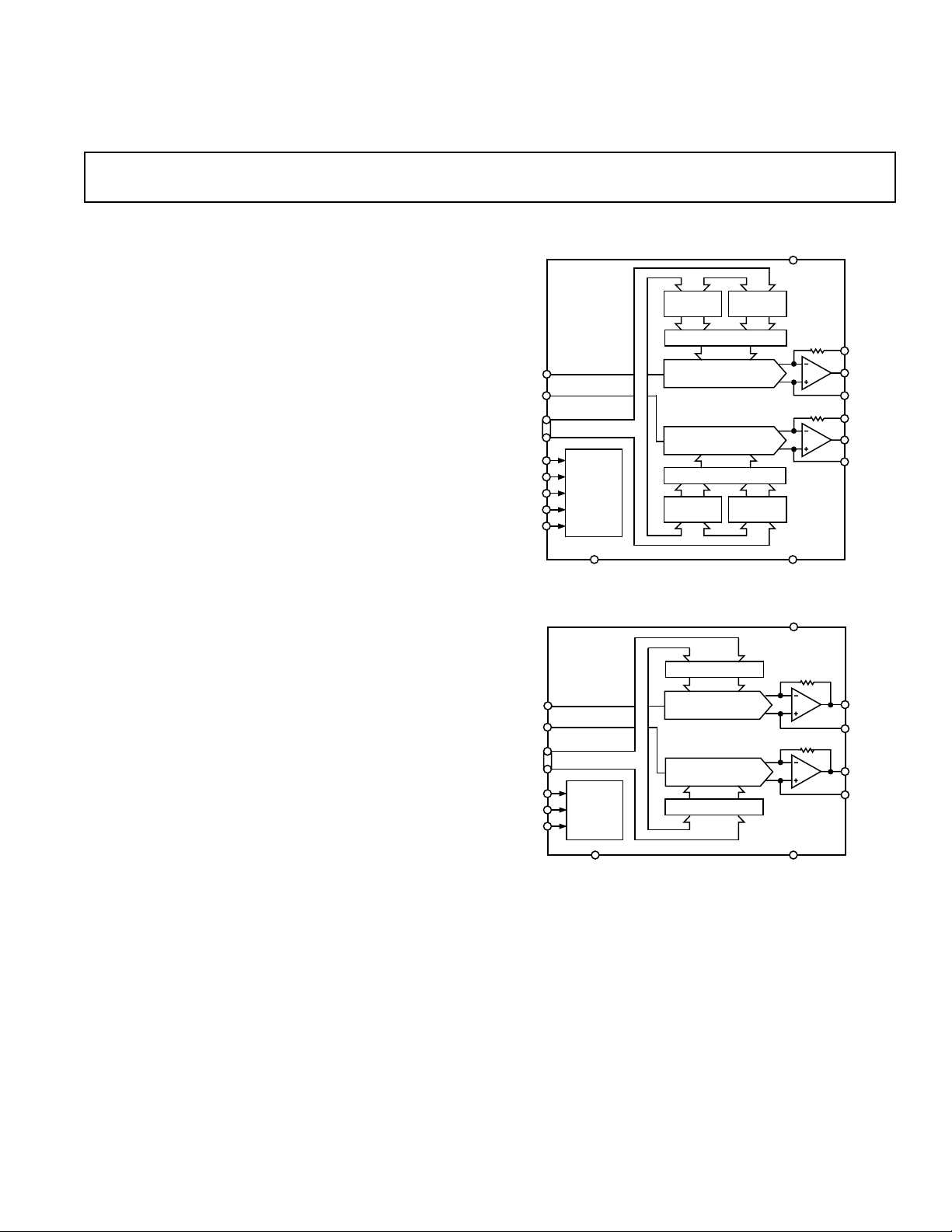
The AD7837/AD7847 is a complete, dual, 12-bit multiplying
digital-to-analog converter with output amplifiers on a monolithic CMOS chip. No external user trims are required to
achieve full specified performance.
Both parts are microprocessor compatible, with high speed data
latches and interface logic. The AD7847 accepts 12-bit parallel
data which is loaded into the respective DAC latch using the
WR input and a separate Chip Select input for each DAC. The
AD7837 has a double-buffered 8-bit bus interface structure
with data loaded to the respective input latch in two write operations. An asynchronous LDAC signal on the AD7837 updates
the DAC latches and analog outputs.
The output amplifiers are capable of developing ±10 V across a
2 kΩ load. They are internally compensated with low input offset voltage due to laser trimming at wafer level.
The amplifier feedback resistors are internally connected to
V
on the AD7847.
OUT
The AD7837/AD7847 is fabricated in Linear Compatible CMOS
2
(LC
MOS), an advanced, mixed technology process that com-
bines precision bipolar circuits with low power CMOS logic.
A novel low leakage configuration (U.S. Patent No. 4,590,456)
ensures low offset errors over the specified temperature range.
Complete, Dual 12-Bit MDACs
AD7837/AD7847
FUNCTIONAL BLOCK DIAGRAMS
V
DD
MS INPUT
LATCH
AD7837
V
REFA
V
REFB
DB0
DB7
LDAC
CS
CONTROL
A0
A1
LOGIC
DGND
AD7847
CONTROL
LOGIC
DGND
MS INPUT
LATCH
DAC LATCH A
DAC LATCH B
V
REFA
V
REFB
DB11
WR
DB0
WR
CSA
CSB
PRODUCT HIGHLIGHTS
1. The AD7837/AD7847 is a dual, 12-bit, voltage-out MDAC
on a single chip. This single chip design offers considerable
space saving and increased reliability over multichip designs.
2. The AD7837 and the AD7847 provide a fast versatile interface to 8-bit or 16-bit data bus structures.
LS INPUT
48
48
LATCH
DAC LATCH A
12
DAC A
DAC B
12
DAC LATCH B
LS INPUT
LATCH
DAC A
DAC B
V
SS
V
DD
V
SS
R
FBA
V
OUTA
AGNDA
R
FBB
V
OUTB
AGNDB
V
OUTA
AGNDA
V
OUTB
AGNDB
REV. C
Information furnished by Analog Devices is believed to be accurate and
reliable. However, no responsibility is assumed by Analog Devices for its
use, nor for any infringements of patents or other rights of third parties
which may result from its use. No license is granted by implication or
otherwise under any patent or patent rights of Analog Devices.
One Technology Way, P.O. Box 9106, Norwood, MA 02062-9106, U.S.A.
Tel: 781/329-4700 World Wide Web Site: http://www.analog.com
Fax: 781/326-8703 © Analog Devices, Inc., 2000

1
AD7837/AD7847–SPECIFICATIONS
= O V. V
Parameter A Version B Version S Version Units Test Conditions/Comments
STATIC PERFORMANCE
Resolution 12 12 12 Bits
Relative Accuracy
Differential Nonlinearity
Zero Code Offset Error
Gain Error
REFERENCE INPUTS
V
V
DIGITAL INPUTS
Input High Voltage, V
Input Low Voltage, V
Input Current ±1 ±1 ±1 µA max Digital Inputs at 0 V and V
Input Capacitance
ANALOG OUTPUTS
DC Output Impedance 0.2 0.2 0.2 Ω typ
Short Circuit Current 11 11 11 mA typ V
POWER REQUIREMENTS
VDD Range 14.25/15.75 14.25/15.75 14.25/15.75 V min/max
VSS Range –14.25/–15.75 –14.25/–15.75 –14.25/–15.75 V min/max
Power Supply Rejection
I
I
AC CHARACTERISTICS
Voltage Output Settling Time 3 3 3 µs typ Settling Time to Within ±1/2 LSB of Final
Slew Rate 11 11 11 V/µs typ
Digital-to-Analog Glitch Impulse 10 10 10 nV secs typ 1 LSB Change Around Major Carry
Channel-to-Channel Isolation
Multiplying Feedthrough Error –90 –90 –90 dB typ V
Unity Gain Small Signal BW 750 750 750 kHz typ V
Full Power BW 175 175 175 kHz typ V
Total Harmonic Distortion –88 –88 –88 dB typ V
Digital Crosstalk 1 1 1 nV secs typ Code Transition from All 0s to All 1s and
Output Noise Voltage @ +25°C See Typical Performance Graphs
Digital Feedthrough 1 1 1 nV secs typ
NOTES
1
Temperature ranges are as follows: A, B Versions, –40°C to +85°C; S Version, –55°C to +125°C.
2
See Terminology.
3
Guaranteed by design and characterization, not production tested.
4
The Devices are functional with VDD/VSS = ± 12 V (See typical performance graphs.).
Specifications subject to change without notice.
= V
REFA
= +10 V, RL = 2 k, CL = 100 pF [V
REFB
2
2
2
±1 ±1/2 ±1 LSB max
±1 ±1 ±1 LSB max Guaranteed Monotonic
connected to RFB AD7837]. All specifications T
OUT
@ +25°C ±2 ±2 ±2 mV max DAC Latch Loaded with All 0s
to T
T
MIN
MAX
2
±4 ±3 ±4 mV max Temperature Coefficient = ±5 µV/°C typ
@ +25°C ±4 ±2 ±4 LSB max DAC Latch Loaded with All 1s
to T
T
MIN
MAX
Input Resistance 8/13 8/13 8/13 kΩ min/max Typical Input Resistance = 10 kΩ
REF
, V
REFA
∆Gain/∆V
∆Gain/∆V
DD
SS
Resistance Matching ±2 ±2 ±2 % max Typically ±0.25%
REFB
INH
INL
3
4
DD
SS
2, 3
±5 ±3 ±5 LSB max Temperature Coefficient = ±2 ppm of
2.4 2.4 2.4 V min
0.8 0.8 0.8 V max
8 8 8 pF max
±0.01 ± 0.01 ± 0.01 % per % max VDD = 15 V ± 5%, V
±0.01 ± 0.01 ± 0.01 % per % max VSS = –15 V ± 5%, V
8 8 8 mA max Outputs Unloaded. Inputs at Thresholds.
6 6 6 mA max Outputs Unloaded. Inputs at Thresholds.
555µs max Value. DAC Latch Alternately Loaded
V
V
REFA
REFB
to V
to V
OUTB
OUTA
–95 –95 –95 dB typ V
–95 –95 –95 dB typ V
(0.1 Hz to 10 Hz) 2 2 2 µV rms typ Amplifier Noise and Johnson Noise of R
(VDD = +15 V 5%, VSS = –15 V 5%, AGNDA = AGNDB = DGND
to T
MIN
FSR/°C typ
OUT
Typically 5 mA
Typically 3 mA
with All 0s and All 1s
REFA
DAC Latches Loaded with All 0s
REFB
DAC Latches Loaded with All 0s
REF
DAC Latch Loaded with All 0s
REF
Latch Loaded with All 1s
REF
Latch Loaded with All 1s
REF
Loaded with All 1s
Vice Versa
unless otherwise noted.)
MAX
DD
Connected to AGND
= –10 V
REF
= +10 V
REF
= 20 V p-p, 10 kHz Sine Wave.
= 20 V p-p, 10 kHz Sine Wave.
= 20 V p-p, 10 kHz Sine Wave.
= 100 mV p-p Sine Wave. DAC
= 20 V p-p Sine Wave. DAC
= 6 V rms, 1 kHz. DAC Latch
FB
–2–
REV. C

AD7837/AD7847
WARNING!
ESD SENSITIVE DEVICE
TIMING CHARACTERISTICS
Limit at T
1, 2, 3
MIN
(VDD = +15 V 5%, VSS = –15 V 5%, AGNDA = AGNDB = DGND = O V)
, T
MAX
Parameter (All Versions) Unit Conditions/Comments
t
1
t
2
t
3
t
4
t
5
4
t
6
4
t
7
4
t
8
NOTES
1
All input signals are specified with tr = tf = 5 ns (10% to 90% of 5 V) and timed from a voltage level of 1.6 V.
2
See Figures 3 and 5.
3
Guaranteed by design and characterization, not production tested.
4
AD7837 only.
ABSOLUTE MAXIMUM RATINGS*
(TA = +25°C unless otherwise noted)
VDD to DGND, AGNDA, AGNDB . . . . . . . –0.3 V to +17 V
1
to DGND, AGNDA, AGNDB . . . . . . . +0.3 V to –17 V
V
SS
V
, V
REFA
to AGNDA, AGNDB
REFB
. . . . . . . . . . . . . . . . . . . . . . . . . . V
AGNDA, AGNDB to DGND . . . . . . . –0.3 V to V
2
V
, V
OUTA
. . . . . . . . . . . . . . . . . . . . . . . . . . V
3
, R
R
FBA
2
to AGNDA, AGNDB
OUTB
3
to AGNDA, AGNDB
FBB
. . . . . . . . . . . . . . . . . . . . . . . . . . V
Digital Inputs to DGND . . . . . . . . . . . –0.3 V to V
Operating Temperature Range
Commercial/Industrial (A, B Versions) . . . –40°C to +85°C
Extended (S Version) . . . . . . . . . . . . . . . . –55°C to +125°C
Storage Temperature Range . . . . . . . . . . . . –65°C to +150°C
Lead Temperature (Soldering, 10 secs) . . . . . . . . . . . . . 300°C
Power Dissipation (Any Package) to +75°C . . . . . . 1000 mW
Derates above +75°C by . . . . . . . . . . . . . . . . . . . . 10 mW/°C
NOTES
1
If VSS is open circuited with VDD and either AGND applied, the VSS pin will float
positive, exceeding the Absolute Maximum Ratings. If this possibility exists, a
Schottky diode connected between VSS and AGND (cathode to AGND) ensures
the Maximum Ratings will be observed.
2
The outputs may be shorted to voltages in this range provided the power dissipation
of the package is not exceeded.
3
AD7837 only.
*Stresses above those listed under Absolute Maximum Ratings may cause perma-
nent damage to the device. This is a stress rating only; functional operation of the
device at these or any other conditions above those listed in the operational sections
of this specification is not implied. Exposure to absolute maximum rating conditions for extended periods may affect device reliability. Only one Absolute
Maximum Rating may be applied at any one time.
0 ns min CS to WR Setup Time
0 ns min CS to WR Hold Time
30 ns min WR Pulsewidth
80 ns min Data Valid to WR Setup Time
0 ns min Data Valid to WR Hold Time
0 ns min Address to WR Setup Time
0 ns min Address to WR Hold Time
50 ns min LDAC Pulsewidth
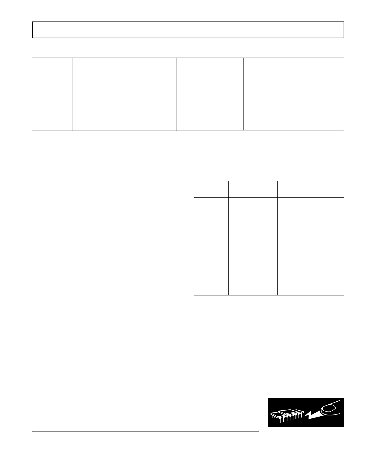
ORDERING GUIDE
Temperature Relative Package
Range Accuracy Option
– 0.3 V to VDD + 0.3 V
SS
– 0.3 V to VDD + 0.3 V
SS
– 0.3 V to VDD + 0.3 V
SS
+ 0.3 V
DD
+ 0.3 V
DD
1
Model
AD7837AN –40°C to +85°C ±1 LSB N-24
AD7837BN –40°C to +85°C ±1/2 LSB N-24
AD7837AR –40°C to +85°C ±1 LSB R-24
AD7837BR –40°C to +85°C ±1/2 LSB R-24
AD7837AQ –40°C to +85°C ±1 LSB Q-24
AD7837BQ –40°C to +85°C ±1/2 LSB Q-24
AD7837SQ –55°C to +125°C ±1 LSB Q-24
AD7847AN –40°C to +85°C ±1 LSB N-24
AD7847BN –40°C to +85°C ±1/2 LSB N-24
AD7847AR –40°C to +85°C ±1 LSB R-24
AD7847BR –40°C to +85°C ±1/2 LSB R-24
AD7847AQ –40°C to +85°C ±1 LSB Q-24
AD7847BQ –40°C to +85°C ±1/2 LSB Q-24
AD7847SQ –55°C to +125°C ±1 LSB Q-24
NOTES
1
To order MIL-STD-883, Class B processed parts, add /883B to part number.
2
N = Plastic DIP; Q = Cerdip; R = SOIC.
2
CAUTION
ESD (electrostatic discharge) sensitive device. Electrostatic charges as high as 4000 V readily
accumulate on the human body and test equipment and can discharge without detection.
Although these devices feature proprietary ESD protection circuitry, permanent damage may
occur on devices subjected to high-energy electrostatic discharges. Therefore, proper ESD
precautions are recommended to avoid performance degradation or loss of functionality.
REV. C
–3–

AD7837/AD7847
TERMINOLOGY
Relative Accuracy (Linearity)
Relative accuracy, or endpoint linearity, is a measure of the
maximum deviation of the DAC transfer function from a
straight line passing through the endpoints. It is measured after
allowing for zero and full-scale errors and is expressed in LSBs
or as a percentage of full-scale reading.
Differential Nonlinearity
Differential nonlinearity is the difference between the measured
change and the ideal 1 LSB change between any two adjacent
codes. A specified differential nonlinearity of ±1 LSB or less
over the operating temperature range ensures monotonicity.
Zero Code Offset Error
Zero code offset error is the error in output voltage from V
or V
with all 0s loaded into the DAC latches. It is due to a
OUTB
OUTA
combination of the DAC leakage current and offset errors in the
output amplifier.
Gain Error
Gain error is a measure of the output error between an ideal
DAC and the actual device output with all 1s loaded. It does
not include offset error.
Total Harmonic Distortion
This is the ratio of the root-mean-square (rms) sum of the harmonics to the fundamental, expressed in dBs.
Multiplying Feedthrough Error
This is an ac error due to capacitive feedthrough from the V
input to V
of the same DAC when the DAC latch is loaded
OUT
REF
with all 0s.
Channel-to-Channel Isolation
This is an ac error due to capacitive feedthrough from the V
input on one DAC to V
on the other DAC. It is measured
OUT
REF
with the DAC latches loaded with all 0s.
Digital Feedthrough
Digital feedthrough is the glitch impulse injected from the digital inputs to the analog output when the data inputs change state,
but the data in the DAC latches is not changed.
For the AD7837, it is measured with LDAC held high. For the
AD7847, it is measured with CSA and CSB held high.
Digital Crosstalk
Digital crosstalk is the glitch impulse transferred to the output
of one converter due to a change in digital code on the DAC
latch of the other converter. It is specified in nV secs.
Digital-to-Analog Glitch Impulse
This is the voltage spike that appears at the output of the DAC
when the digital code changes, before the output settles to its
final value. The energy in the glitch is specified in nV secs and is
measured for a 1 LSB change around the major carry transition
(0111 1111 1111 to 1000 0000 0000 and vice versa).
Unity Gain Small Signal Bandwidth
This is the frequency at which the small signal voltage output
from the output amplifier is 3 dB below its dc level. It is measured with the DAC latch loaded with all 1s.
Full Power Bandwidth
This is the maximum frequency for which a sinusoidal input
signal will produce full output at rated load with a distortion
less than 3%. It is measured with the DAC latch loaded with
all 1s.
AD7837 PIN FUNCTION DESCRIPTION (DIP AND SOIC PIN NUMBERS)
Pin Mnemonic Description
1 CS Chip Select. Active low logic input. The device is selected when this input is active.
2R
3V
4V
FBA
REFA
OUTA
Amplifier Feedback Resistor for DAC A.
Reference Input Voltage for DAC A. This may be an ac or dc signal.
Analog Output Voltage from DAC A.
5 AGNDA Analog Ground for DAC A.
6V
7V
DD
SS
Positive Power Supply.
Negative Power Supply.
8 AGNDB Analog Ground for DAC B.
9V
10 V
OUTB
REFB
Analog Output Voltage from DAC B.
Reference Input Voltage for DAC B. This may be an ac or dc signal.
11 DGND Digital Ground. Ground reference for digital circuitry.
12 R
FBB
Amplifier Feedback Resistor for DAC B.
13 WR Write Input. WR is an active low logic input which is used in conjunction with CS, A0 and A1 to
write data to the input latches.
14 LDAC DAC Update Logic Input. Data is transferred from the input latches to the DAC latches when LDAC
is taken low.
15 A1 Address Input. Most significant address input for input latches (see Table II).
16 A0 Address Input. Least significant address input for input latches (see Table II).
17–20 DB7–DB4 Data Bit 7 to Data Bit 4.
21–24 DB3–DB0 Data Bit 3 to Data Bit 0 (LSB) or Data Bit 11 (MSB) to Data Bit 8.
–4–
REV. C
 Loading...