

LC2MOS
a
FEATURES
Two 12-Bit MDACs with Output Amplifiers
4-Quadrant Multiplication
Space-Saving 0.3", 24-Lead DIP and 24-Terminal
SOIC Package
Parallel Loading Structure: AD7847
(8 + 4) Loading Structure: AD7837
APPLICATIONS
Automatic Test Equipment
Function Generation
Waveform Reconstruction
Programmable Power Supplies
Synchro Applications
GENERAL DESCRIPTION
The AD7837/AD7847 is a complete, dual, 12-bit multiplying
digital-to-analog converter with output amplifiers on a monolithic CMOS chip. No external user trims are required to
achieve full specified performance.
Both parts are microprocessor compatible, with high speed data
latches and interface logic. The AD7847 accepts 12-bit parallel
data which is loaded into the respective DAC latch using the
WR input and a separate Chip Select input for each DAC. The
AD7837 has a double-buffered 8-bit bus interface structure
with data loaded to the respective input latch in two write operations. An asynchronous LDAC signal on the AD7837 updates
the DAC latches and analog outputs.
The output amplifiers are capable of developing ±10 V across a
2 kΩ load. They are internally compensated with low input offset voltage due to laser trimming at wafer level.
The amplifier feedback resistors are internally connected to
V
on the AD7847.
OUT
The AD7837/AD7847 is fabricated in Linear Compatible CMOS
2
(LC
MOS), an advanced, mixed technology process that com-
bines precision bipolar circuits with low power CMOS logic.
A novel low leakage configuration (U.S. Patent No. 4,590,456)
ensures low offset errors over the specified temperature range.
Complete, Dual 12-Bit MDACs
AD7837/AD7847
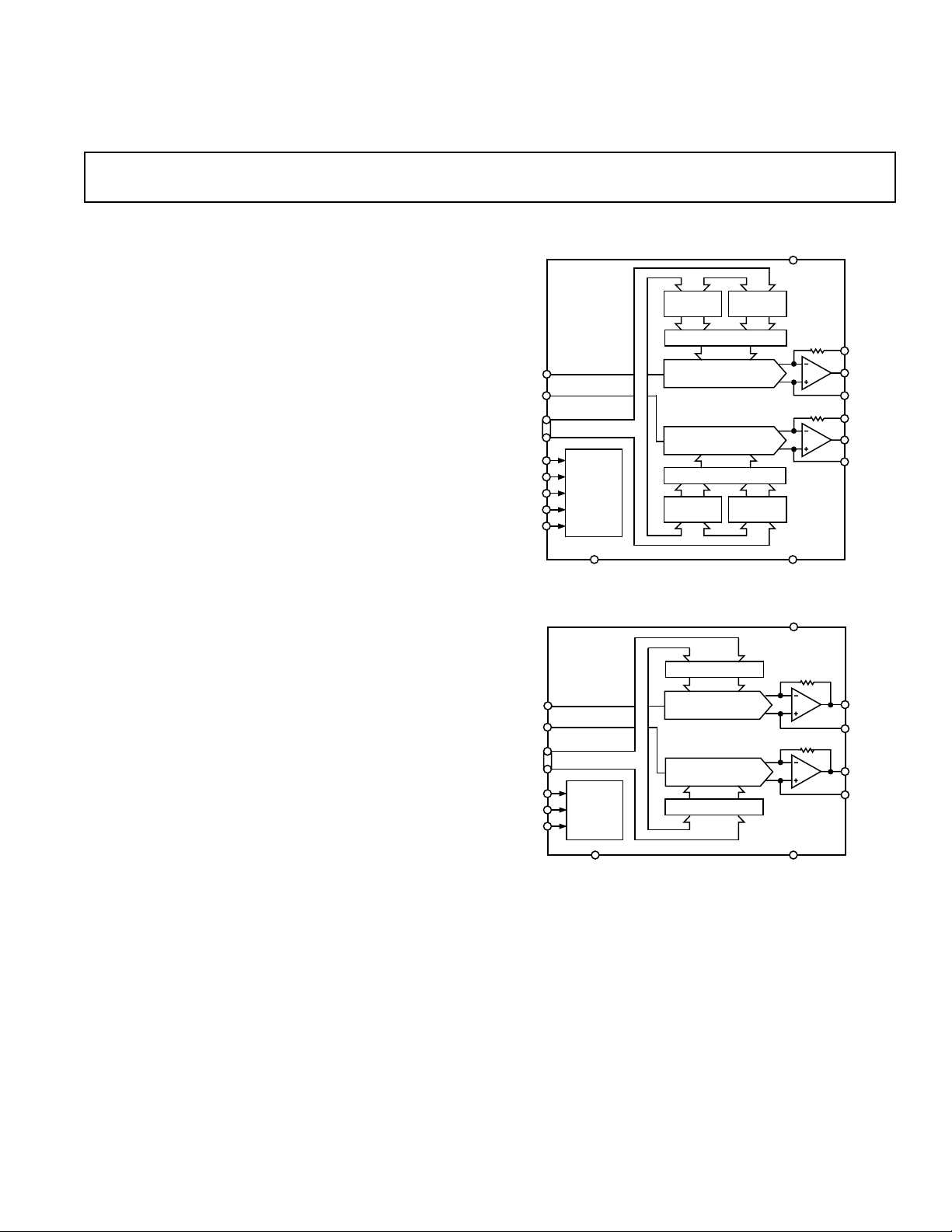
FUNCTIONAL BLOCK DIAGRAMS
V
DD
MS INPUT
LATCH
AD7837
V
REFA
V
REFB
DB0
DB7
LDAC
CS
CONTROL
A0
A1
LOGIC
DGND
AD7847
CONTROL
LOGIC
DGND
MS INPUT
LATCH
DAC LATCH A
DAC LATCH B
V
REFA
V
REFB
DB11
WR
DB0
WR
CSA
CSB
PRODUCT HIGHLIGHTS
1. The AD7837/AD7847 is a dual, 12-bit, voltage-out MDAC
on a single chip. This single chip design offers considerable
space saving and increased reliability over multichip designs.
2. The AD7837 and the AD7847 provide a fast versatile interface to 8-bit or 16-bit data bus structures.
LS INPUT
48
48
LATCH
DAC LATCH A
12
DAC A
DAC B
12
DAC LATCH B
LS INPUT
LATCH
DAC A
DAC B
V
SS
V
DD
V
SS
R
FBA
V
OUTA
AGNDA
R
FBB
V
OUTB
AGNDB
V
OUTA
AGNDA
V
OUTB
AGNDB
REV. C
Information furnished by Analog Devices is believed to be accurate and
reliable. However, no responsibility is assumed by Analog Devices for its
use, nor for any infringements of patents or other rights of third parties
which may result from its use. No license is granted by implication or
otherwise under any patent or patent rights of Analog Devices.
One Technology Way, P.O. Box 9106, Norwood, MA 02062-9106, U.S.A.
Tel: 781/329-4700 World Wide Web Site: http://www.analog.com
Fax: 781/326-8703 © Analog Devices, Inc., 2000

1
AD7837/AD7847–SPECIFICATIONS
= O V. V
Parameter A Version B Version S Version Units Test Conditions/Comments
STATIC PERFORMANCE
Resolution 12 12 12 Bits
Relative Accuracy
Differential Nonlinearity
Zero Code Offset Error
Gain Error
REFERENCE INPUTS
V
V
DIGITAL INPUTS
Input High Voltage, V
Input Low Voltage, V
Input Current ±1 ±1 ±1 µA max Digital Inputs at 0 V and V
Input Capacitance
ANALOG OUTPUTS
DC Output Impedance 0.2 0.2 0.2 Ω typ
Short Circuit Current 11 11 11 mA typ V
POWER REQUIREMENTS
VDD Range 14.25/15.75 14.25/15.75 14.25/15.75 V min/max
VSS Range –14.25/–15.75 –14.25/–15.75 –14.25/–15.75 V min/max
Power Supply Rejection
I
I
AC CHARACTERISTICS
Voltage Output Settling Time 3 3 3 µs typ Settling Time to Within ±1/2 LSB of Final
Slew Rate 11 11 11 V/µs typ
Digital-to-Analog Glitch Impulse 10 10 10 nV secs typ 1 LSB Change Around Major Carry
Channel-to-Channel Isolation
Multiplying Feedthrough Error –90 –90 –90 dB typ V
Unity Gain Small Signal BW 750 750 750 kHz typ V
Full Power BW 175 175 175 kHz typ V
Total Harmonic Distortion –88 –88 –88 dB typ V
Digital Crosstalk 1 1 1 nV secs typ Code Transition from All 0s to All 1s and
Output Noise Voltage @ +25°C See Typical Performance Graphs
Digital Feedthrough 1 1 1 nV secs typ
NOTES
1
Temperature ranges are as follows: A, B Versions, –40°C to +85°C; S Version, –55°C to +125°C.
2
See Terminology.
3
Guaranteed by design and characterization, not production tested.
4
The Devices are functional with VDD/VSS = ± 12 V (See typical performance graphs.).
Specifications subject to change without notice.
= V
REFA
= +10 V, RL = 2 k, CL = 100 pF [V
REFB
2
2
2
±1 ±1/2 ±1 LSB max
±1 ±1 ±1 LSB max Guaranteed Monotonic
connected to RFB AD7837]. All specifications T
OUT
@ +25°C ±2 ±2 ±2 mV max DAC Latch Loaded with All 0s
to T
T
MIN
MAX
2
±4 ±3 ±4 mV max Temperature Coefficient = ±5 µV/°C typ
@ +25°C ±4 ±2 ±4 LSB max DAC Latch Loaded with All 1s
to T
T
MIN
MAX
Input Resistance 8/13 8/13 8/13 kΩ min/max Typical Input Resistance = 10 kΩ
REF
, V
REFA
∆Gain/∆V
∆Gain/∆V
DD
SS
Resistance Matching ±2 ±2 ±2 % max Typically ±0.25%
REFB
INH
INL
3
4
DD
SS
2, 3
±5 ±3 ±5 LSB max Temperature Coefficient = ±2 ppm of
2.4 2.4 2.4 V min
0.8 0.8 0.8 V max
8 8 8 pF max
±0.01 ± 0.01 ± 0.01 % per % max VDD = 15 V ± 5%, V
±0.01 ± 0.01 ± 0.01 % per % max VSS = –15 V ± 5%, V
8 8 8 mA max Outputs Unloaded. Inputs at Thresholds.
6 6 6 mA max Outputs Unloaded. Inputs at Thresholds.
555µs max Value. DAC Latch Alternately Loaded
V
V
REFA
REFB
to V
to V
OUTB
OUTA
–95 –95 –95 dB typ V
–95 –95 –95 dB typ V
(0.1 Hz to 10 Hz) 2 2 2 µV rms typ Amplifier Noise and Johnson Noise of R
(VDD = +15 V 5%, VSS = –15 V 5%, AGNDA = AGNDB = DGND
to T
MIN
FSR/°C typ
OUT
Typically 5 mA
Typically 3 mA
with All 0s and All 1s
REFA
DAC Latches Loaded with All 0s
REFB
DAC Latches Loaded with All 0s
REF
DAC Latch Loaded with All 0s
REF
Latch Loaded with All 1s
REF
Latch Loaded with All 1s
REF
Loaded with All 1s
Vice Versa
unless otherwise noted.)
MAX
DD
Connected to AGND
= –10 V
REF
= +10 V
REF
= 20 V p-p, 10 kHz Sine Wave.
= 20 V p-p, 10 kHz Sine Wave.
= 20 V p-p, 10 kHz Sine Wave.
= 100 mV p-p Sine Wave. DAC
= 20 V p-p Sine Wave. DAC
= 6 V rms, 1 kHz. DAC Latch
FB
–2–
REV. C
AD7837/AD7847
WARNING!
ESD SENSITIVE DEVICE
TIMING CHARACTERISTICS
Limit at T
1, 2, 3
MIN
(VDD = +15 V 5%, VSS = –15 V 5%, AGNDA = AGNDB = DGND = O V)
, T
MAX
Parameter (All Versions) Unit Conditions/Comments
t
1
t
2
t
3
t
4
t
5
4
t
6
4
t
7
4
t
8
NOTES
1
All input signals are specified with tr = tf = 5 ns (10% to 90% of 5 V) and timed from a voltage level of 1.6 V.
2
See Figures 3 and 5.
3
Guaranteed by design and characterization, not production tested.
4
AD7837 only.
ABSOLUTE MAXIMUM RATINGS*
(TA = +25°C unless otherwise noted)
VDD to DGND, AGNDA, AGNDB . . . . . . . –0.3 V to +17 V
1
to DGND, AGNDA, AGNDB . . . . . . . +0.3 V to –17 V
V
SS
V
, V
REFA
to AGNDA, AGNDB
REFB
. . . . . . . . . . . . . . . . . . . . . . . . . . V
AGNDA, AGNDB to DGND . . . . . . . –0.3 V to V
2
V
, V
OUTA
. . . . . . . . . . . . . . . . . . . . . . . . . . V
3
, R
R
FBA
2
to AGNDA, AGNDB
OUTB
3
to AGNDA, AGNDB
FBB
. . . . . . . . . . . . . . . . . . . . . . . . . . V
Digital Inputs to DGND . . . . . . . . . . . –0.3 V to V
Operating Temperature Range
Commercial/Industrial (A, B Versions) . . . –40°C to +85°C
Extended (S Version) . . . . . . . . . . . . . . . . –55°C to +125°C
Storage Temperature Range . . . . . . . . . . . . –65°C to +150°C
Lead Temperature (Soldering, 10 secs) . . . . . . . . . . . . . 300°C
Power Dissipation (Any Package) to +75°C . . . . . . 1000 mW
Derates above +75°C by . . . . . . . . . . . . . . . . . . . . 10 mW/°C
NOTES
1
If VSS is open circuited with VDD and either AGND applied, the VSS pin will float
positive, exceeding the Absolute Maximum Ratings. If this possibility exists, a
Schottky diode connected between VSS and AGND (cathode to AGND) ensures
the Maximum Ratings will be observed.
2
The outputs may be shorted to voltages in this range provided the power dissipation
of the package is not exceeded.
3
AD7837 only.
*Stresses above those listed under Absolute Maximum Ratings may cause perma-
nent damage to the device. This is a stress rating only; functional operation of the
device at these or any other conditions above those listed in the operational sections
of this specification is not implied. Exposure to absolute maximum rating conditions for extended periods may affect device reliability. Only one Absolute
Maximum Rating may be applied at any one time.
0 ns min CS to WR Setup Time
0 ns min CS to WR Hold Time
30 ns min WR Pulsewidth
80 ns min Data Valid to WR Setup Time
0 ns min Data Valid to WR Hold Time
0 ns min Address to WR Setup Time
0 ns min Address to WR Hold Time
50 ns min LDAC Pulsewidth
ORDERING GUIDE
Temperature Relative Package
Range Accuracy Option
– 0.3 V to VDD + 0.3 V
SS
– 0.3 V to VDD + 0.3 V
SS
– 0.3 V to VDD + 0.3 V
SS
+ 0.3 V
DD
+ 0.3 V
DD
1
Model
AD7837AN –40°C to +85°C ±1 LSB N-24
AD7837BN –40°C to +85°C ±1/2 LSB N-24
AD7837AR –40°C to +85°C ±1 LSB R-24
AD7837BR –40°C to +85°C ±1/2 LSB R-24
AD7837AQ –40°C to +85°C ±1 LSB Q-24
AD7837BQ –40°C to +85°C ±1/2 LSB Q-24
AD7837SQ –55°C to +125°C ±1 LSB Q-24
AD7847AN –40°C to +85°C ±1 LSB N-24
AD7847BN –40°C to +85°C ±1/2 LSB N-24
AD7847AR –40°C to +85°C ±1 LSB R-24
AD7847BR –40°C to +85°C ±1/2 LSB R-24
AD7847AQ –40°C to +85°C ±1 LSB Q-24
AD7847BQ –40°C to +85°C ±1/2 LSB Q-24
AD7847SQ –55°C to +125°C ±1 LSB Q-24
NOTES
1
To order MIL-STD-883, Class B processed parts, add /883B to part number.
2
N = Plastic DIP; Q = Cerdip; R = SOIC.
2
CAUTION
ESD (electrostatic discharge) sensitive device. Electrostatic charges as high as 4000 V readily
accumulate on the human body and test equipment and can discharge without detection.
Although these devices feature proprietary ESD protection circuitry, permanent damage may
occur on devices subjected to high-energy electrostatic discharges. Therefore, proper ESD
precautions are recommended to avoid performance degradation or loss of functionality.
REV. C
–3–

AD7837/AD7847
TERMINOLOGY
Relative Accuracy (Linearity)
Relative accuracy, or endpoint linearity, is a measure of the
maximum deviation of the DAC transfer function from a
straight line passing through the endpoints. It is measured after
allowing for zero and full-scale errors and is expressed in LSBs
or as a percentage of full-scale reading.
Differential Nonlinearity
Differential nonlinearity is the difference between the measured
change and the ideal 1 LSB change between any two adjacent
codes. A specified differential nonlinearity of ±1 LSB or less
over the operating temperature range ensures monotonicity.
Zero Code Offset Error
Zero code offset error is the error in output voltage from V
or V
with all 0s loaded into the DAC latches. It is due to a
OUTB
OUTA
combination of the DAC leakage current and offset errors in the
output amplifier.
Gain Error
Gain error is a measure of the output error between an ideal
DAC and the actual device output with all 1s loaded. It does
not include offset error.
Total Harmonic Distortion
This is the ratio of the root-mean-square (rms) sum of the harmonics to the fundamental, expressed in dBs.
Multiplying Feedthrough Error
This is an ac error due to capacitive feedthrough from the V
input to V
of the same DAC when the DAC latch is loaded
OUT
REF
with all 0s.
Channel-to-Channel Isolation
This is an ac error due to capacitive feedthrough from the V
input on one DAC to V
on the other DAC. It is measured
OUT
REF
with the DAC latches loaded with all 0s.
Digital Feedthrough
Digital feedthrough is the glitch impulse injected from the digital inputs to the analog output when the data inputs change state,
but the data in the DAC latches is not changed.
For the AD7837, it is measured with LDAC held high. For the
AD7847, it is measured with CSA and CSB held high.
Digital Crosstalk
Digital crosstalk is the glitch impulse transferred to the output
of one converter due to a change in digital code on the DAC
latch of the other converter. It is specified in nV secs.
Digital-to-Analog Glitch Impulse
This is the voltage spike that appears at the output of the DAC
when the digital code changes, before the output settles to its
final value. The energy in the glitch is specified in nV secs and is
measured for a 1 LSB change around the major carry transition
(0111 1111 1111 to 1000 0000 0000 and vice versa).
Unity Gain Small Signal Bandwidth
This is the frequency at which the small signal voltage output
from the output amplifier is 3 dB below its dc level. It is measured with the DAC latch loaded with all 1s.
Full Power Bandwidth
This is the maximum frequency for which a sinusoidal input
signal will produce full output at rated load with a distortion
less than 3%. It is measured with the DAC latch loaded with
all 1s.
AD7837 PIN FUNCTION DESCRIPTION (DIP AND SOIC PIN NUMBERS)
Pin Mnemonic Description
1 CS Chip Select. Active low logic input. The device is selected when this input is active.
2R
3V
4V
FBA
REFA
OUTA
Amplifier Feedback Resistor for DAC A.
Reference Input Voltage for DAC A. This may be an ac or dc signal.
Analog Output Voltage from DAC A.
5 AGNDA Analog Ground for DAC A.
6V
7V
DD
SS
Positive Power Supply.
Negative Power Supply.
8 AGNDB Analog Ground for DAC B.
9V
10 V
OUTB
REFB
Analog Output Voltage from DAC B.
Reference Input Voltage for DAC B. This may be an ac or dc signal.
11 DGND Digital Ground. Ground reference for digital circuitry.
12 R
FBB
Amplifier Feedback Resistor for DAC B.
13 WR Write Input. WR is an active low logic input which is used in conjunction with CS, A0 and A1 to
write data to the input latches.
14 LDAC DAC Update Logic Input. Data is transferred from the input latches to the DAC latches when LDAC
is taken low.
15 A1 Address Input. Most significant address input for input latches (see Table II).
16 A0 Address Input. Least significant address input for input latches (see Table II).
17–20 DB7–DB4 Data Bit 7 to Data Bit 4.
21–24 DB3–DB0 Data Bit 3 to Data Bit 0 (LSB) or Data Bit 11 (MSB) to Data Bit 8.
–4–
REV. C

AD7837/AD7847
AD7847 PIN FUNCTION DESCRIPTION (DIP AND SOIC PIN NUMBERS)
Pin Mnemonic Description
11 CSA Chip Select Input for DAC A. Active low logic input. DAC A is selected when this input is low.
12 CSB Chip Select Input for DAC B. Active low logic input. DAC B is selected when this input is low.
13V
14V
REFA
OUTA
15 AGNDA Analog Ground for DAC A.
16V
17V
DD
SS
18 AGNDB Analog Ground for DAC B.
19V
10 V
OUTB
REFB
11 DGND Digital Ground.
12 DB11 Data Bit 11 (MSB).
13 WR Write Input. WR is a positive edge triggered input which is used in conjunction with CSA and CSB
14–24 DB10–DB0 Data Bit 10 to Data Bit 0 (LSB).
AD7837 PIN CONFIGURATION AD7847 PIN CONFIGURATION
Reference Input Voltage for DAC A. This may be an ac or dc signal.
Analog Output Voltage from DAC A.
Positive Power Supply.
Negative Power Supply.
Analog Output Voltage from DAC B.
Reference Input Voltage for DAC B. This may be an ac or dc signal.
to write data to the DAC latches.
DIP AND SOIC DIP AND SOIC
CS
R
FBA
V
REFA
V
OUTA
AGNDA
V
V
AGNDB
V
OUTB
V
REFB
DGND
R
FBB
DD
SS
1
2
3
4
5
AD7837
6
TOP VIEW
(Not to Scale)
7
8
9
10
11
12
24
DB0
23
DB1
22
DB2
21
DB3
20
DB4
19
DB5
18
DB6
17
DB7
16
A0
15
A1
14
LDAC
13
WR
CSA
CSB
V
REFA
V
OUTA
AGNDA
V
V
AGNDB
V
OUTB
V
REFB
DGND
DB11
DD
SS
1
2
3
4
5
AD7847
6
TOP VIEW
(Not to Scale)
7
8
9
10
11
12
24
DB0
23
DB1
22
DB2
21
DB3
20
DB4
19
DB5
18
DB6
17
DB7
16
DB8
15
DB9
DB10
14
13
WR
REV. C
–5–

AD7837/AD7847–Typical Performance Graphs
FREQUENCY – kHz
THD – dB
0.1
100
110
–40
VDD = +15V
VSS = –15V
V
REF
= 6V rms
DAC CODE = 111...111
–50
–60
–70
–80
–90
–100
10
0
–10
VDD = +15V
GAIN – dB
VSS = –15V
= +20Vp–p
V
REF
–20
DAC CODE = 111...111
–30
4
10
5
10
FREQUENCY – Hz
10
6
7
10
Figure 1. Frequency Response
0.5
0.4
0.3
0.2
ERROR – LSB
0.1
0.0
0
11 13 15 17
VDD/VSS – Volts
V
= 7.5V
REF
INL
DNL
Figure 4. Linearity vs. Power Supply
25
20
15
– Volts p–p
10
OUT
V
5
0
10
VDD = +15V
= –15V
V
SS
V
= +20Vp–p @ 1kHz
REF
DAC CODE = 111...111
100 1k 10k
LOAD RESISTANCE –
Figure 2. Output Voltage Swing vs.
Resistive Load
400
300
200
100
NOISE SPECTRAL DENSITY – nV/ Hz
0
0.01
VDD = +15V
VSS = –15V
V
= 0V
REF
DAC CODE = 111...111
0.1 1 100
FREQUENCY – Hz
10
Figure 5. Noise Spectral Density vs.
Frequency
–0.2
–0.4
–0.6
ERROR – LSB
–0.2
–0.4
–0.6
0.6
0.4
0.2
0
0.6
0.4
0.2
0
0
VDD = +15V
V
= –15V
SS
2048 4095
CODE
DAC A
DAC B
Figure 3. DAC-to-DAC Linearity
Matching
Figure 6. THD vs. Frequency
Figure 7. Multiplying Feedthrough
Error vs. Frequency
–50
–60
VDD = +15V
VSS = –15V
= 20V p-p
V
–70
–80
FEEDTHROUGH – dB
–90
–100
REF
DAC CODE = 000...000
0.1 1 100
10 1000
FREQUENCY – kHz
FULL SCALE
V
OUT
ZERO SCALE
HORIZ 2s/ DIV
VERT 2V/ DIV
Figure 8. Large Signal Pulse
Response
A1 –0.01V
200mV 50mV
B
w
L
2s
Figure 9. Small Signal Pulse
Response
–6–
REV. C

AD7837/AD7847
CIRCUIT INFORMATION
D/A SECTION
A simplified circuit diagram for one of the D/A converters and
output amplifier is shown in Figure 10.
A segmented scheme is used whereby the 2 MSBs of the 12-bit
data word are decoded to drive the three switches A-C. The
remaining 10 bits drive the switches (S0–S9) in a standard R-2R
ladder configuration.
Each of the switches A–C steers 1/4 of the total reference current with the remaining 1/4 passing through the R-2R section.
The output amplifier and feedback resistor perform the current
to voltage conversion giving
V
= – D × V
OUT
REF
where D is the fractional representation of the digital word. (D
can be set from 0 to 4095/4096.)
The output amplifier can maintain ±10 V across a 2 kΩ load. It
is internally compensated and settles to 0.01% FSR (1/2 LSB)
in less than 5 µs. Note that on the AD7837, V
nected externally to R
V
REF
.
FB
R
R
2R2R2R2R
SHOWN FOR ALL 1s ON DAC
R
2R
S8S9ABC
2R 2R
S0
must be con-
OUT
R/2
V
OUT
AGND
Figure 10. D/A Simplified Circuit Diagram
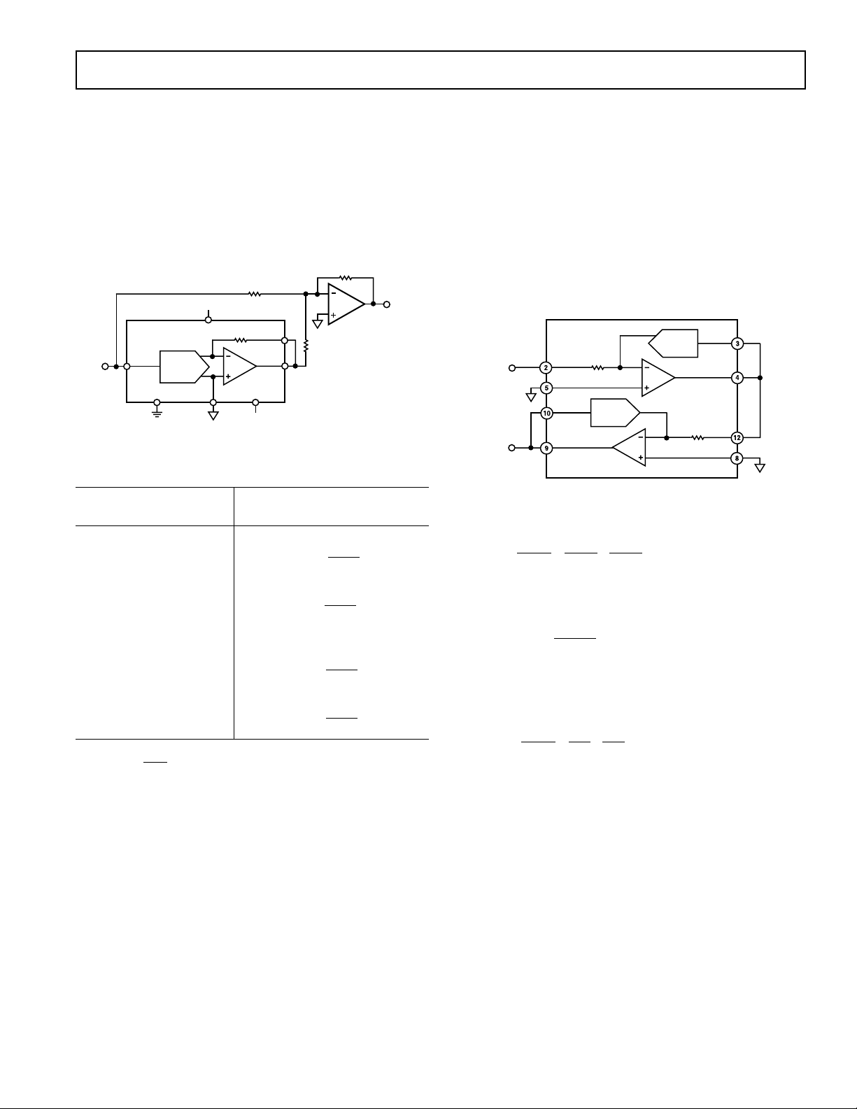
INTERFACE LOGIC INFORMATION—AD7847
The input control logic for the AD7847 is shown in Figure 11.
The part contains a 12-bit latch for each DAC. It can be treated
as two independent DACs, each with its own CS input and a common WR input. CSA and WR control the loading of data to the
DAC A latch, while CSB and WR control the loading of the
DAC B latch. The latches are edge triggered so that input data
is latched to the respective latch on the rising edge of WR. If CSA
and CSB are both low and WR is taken high, the same data will
be latched to both DAC latches. The control logic truth table is
shown in Table I, while the write cycle timing diagram for the
part is shown in Figure 12.
CSA
WR
CSB
DAC A LATCH
DAC B LATCH
Figure 11. AD7847 Input Control Logic
Table I. AD7847 Truth Table
CC
CSA CSB WR Function
CC
X X 1 No Data Transfer
1 1 X No Data Transfer
01 g Data Latched to DAC A
10 g Data Latched to DAC B
00 g Data Latched to Both DACs
g 1 0 Data Latched to DAC A
1 g 0 Data Latched to DAC B
gg 0 Data Latched to Both DACs
X = Don’t Care. g = Rising Edge Triggered.
CSA, CSB
WR
DATA
t
1
t
3
t
4
VALID
DATA
t
2
t
5
Figure 12. AD7847 Write Cycle Timing Diagram
INTERFACE LOGIC INFORMATION—AD7837
The input loading structure on the AD7837 is configured for
interfacing to microprocessors with an 8-bit-wide data bus. The
part contains two 12-bit latches per DAC—an input latch and
a DAC latch. Each input latch is further subdivided into a leastsignificant 8-bit latch and a most-significant 4-bit latch. Only the
data held in the DAC latches determines the outputs from the part.
The input control logic for the AD7837 is shown in Figure 13,
while the write cycle timing diagram is shown in Figure 14.
LDAC
WR
CS
A0
DAC A
LATCH
12
4
DAC A MS
INPUT
LATCH
A1
8
DAC A LS
INPUT
LATCH
DB7 DB0
4
DAC B LS
INPUT
LATCH
8
DAC B
LATCH
12
DAC B LS
8
INPUT
LATCH
Figure 13. AD7837 Input Control Logic
REV. C
–7–

AD7837/AD7847
A0/A1
CS
WR
DATA
LDAC
ADDRESS DATA
t
6
t
1
t
3
t
4
VALID
DATA
t
7
t
2
t
5
t
8
Figure 14. AD7837 Write Cycle Timing Diagram
CS, WR, A0 and A1 control the loading of data to the input
latches. The eight data inputs accept right-justified data. Data
can be loaded to the input latches in any sequence. Provided that
LDAC is held high, there is no analog output change as a result
of loading data to the input latches. Address lines A0 and A1
determine which latch data is loaded to when CS and WR are low.
The control logic truth table for the part is shown in Table II.
Table II. AD7837 Truth Table
CS WR A1 A0 LDAC Function
1 X X X 1 No Data Transfer
X 1 X X 1 No Data Transfer
0 0 0 0 1 DAC A LS Input Latch Transparent
0 0 0 1 1 DAC A MS Input Latch Transparent
0 0 1 0 1 DAC B LS Input Latch Transparent
0 0 1 1 1 DAC B MS Input Latch Transparent
1 1 X X 0 DAC A and DAC B DAC Latches
Updated Simultaneously from the
Respective Input Latches
X = Don’t Care.
The LDAC input controls the transfer of 12-bit data from the
input latches to the DAC latches. When LDAC is taken low, both
DAC latches, and hence both analog outputs, are updated at
the same time. The data in the DAC latches is held on the rising
edge of LDAC. The LDAC input is asynchronous and independent of WR. This is useful in many applications especially in the
simultaneous updating of multiple AD7837s. However, care must
be taken while exercising LDAC during a write cycle. If an LDAC
operation overlaps a CS and WR operation, there is a possibility
of invalid data being latched to the output. To avoid this, LDAC
must remain low after CS or WR return high for a period equal
to or greater than t
, the minimum LDAC pulsewidth.
8
UNIPOLAR BINARY OPERATION
Figure 15 shows DAC A on the AD7837/AD7847 connected
for unipolar binary operation. Similar connections apply for
DAC B. When V
is an ac signal, the circuit performs 2-quad-
IN
rant multiplication. The code table for this circuit is shown in
Table III. Note that on the AD7847 the feedback resistor R
internally connected to V
AD7837
AD7847
V
REFA
V
IN
DAC A
DGND
OUT
V
DD
V
DD
AGNDA
.
R
FBA
*
V
OUTA
V
SS
V
SS
*INTERNALLY
CONNECTED
ON AD7847
is
FB
V
OUT
Figure 15. Unipolar Binary Operation
Table III. Unipolar Code Table
DAC Latch Contents
MSB LSB Analog Output, V
1111 1111 1111
1000 0000 0000
0000 0000 0001
–VIN×
–VIN×
–VIN×
4095
4096
2048
4096
4096
1
OUT
= –1/2 V
IN
0000 0000 0000 0 V
V
Note 1 LSB =
4096
IN
.
–8–
REV. C
AD7837/AD7847
BIPOLAR OPERATION
(4-QUADRANT MULTIPLICATION)
Figure 16 shows the AD7837/AD7847 connected for bipolar
operation. The coding is offset binary as shown in Table IV.
When V
is an ac signal, the circuit performs 4-quadrant multi-
IN
plication. To maintain the gain error specifications, resistors R1,
R2 and R3 should be ratio matched to 0.01%. Note that on the
AD7847 the feedback resistor R
V
.
OUT
V
DD
DAC A
AGNDA
V
DD
AD7837
AD7847
V
V
IN
REFA
DGND
is internally connected to
FB
R2
R3
10k
20k
AD711
R1
20k
V
V
V
SS
SS
R
OUTA
FBA
*
*INTERNALLY
CONNECTED
ON AD7847
V
OUT
Figure 16. Bipolar Offset Binary Operation
Table IV. Bipolar Code Table
DAC Latch Contents
MSB LSB Analog Output, V
OUT
APPLICATIONS
PROGRAMMABLE GAIN AMPLIFIER (PGA)
The dual DAC/amplifier combination along with access to R
FB
make the AD7837 ideal as a programmable gain amplifier. In this
application, the DAC functions as a programmable resistor in the
amplifier feedback loop. This type of configuration is shown
in Figure 17 and is suitable for ac gain control. The circuit consists of two PGAs in series. Use of a dual configuration provides
greater accuracy over a wider dynamic range than a single PGA
solution. The overall system gain is the product of the individual
gain stages. The effective gains for each stage are controlled by
the DAC codes. As the code decreases, the effective DAC
resistance increases, and so the gain also increases.
V
AD7837
AGNDB
V
REFA
OUTA
R
FBB
DAC A
R
V
IN
V
OUT
FBA
AGNDA
V
REFB
V
OUTB
DAC B
Figure 17. Dual PGA Circuit
The transfer function is given by
1111 1111 1111
+VIN×
1000 0000 0001
+VIN×
1000 0000 0000 0 V
0111 1111 1111
–VIN×
0000 0000 0000
–VIN×
V
Note 1 LSB =
2048
IN
.
2048
2048
2048
2048
2047
2048
1
1
= –V
where R
EQA
V
, R
V
R
OUT
=
R
IN
are the effective DAC resistances controlled
EQB
EQA
FBA
R
EQB
×
R
FBB
(1)
by the digital input code:
12
2
R
IN
(2)
N
where R
REQ=
is the DAC input resistance and is equal to RFB and
IN
N = DAC input code in decimal.
The transfer function in (1) thus simplifies to
IN
where N
V
OUT
V
IN
= DAC A input code in decimal and NB = DAC B
A
12
12
2
=
2
×
N
N
A
B
(3)
input code in decimal.
N
, NB may be programmed between 1 and (212–1). The zero
A
code is not allowed as it results in an open loop amplifier
response. To minimize errors, the digital codes N
and N
A
B
should be chosen to be equal to or as close as possible to each
other to achieve the required gain.
REV. C
–9–

AD7837/AD7847
ANALOG PANNING CIRCUIT
In audio applications it is often necessary to digitally “pan” or
split a single signal source into a two-channel signal while maintaining the total power delivered to both channels constant. This
may be done very simply by feeding the signal into the V
REF
input of both DACs. The digital codes are chosen such that the
code applied to DAC B is the two's complement of that applied
to DAC A. In this way the signal may be panned between both
channels as the digital code is changed. The total power variation with this arrangement is 3 dB.
For applications which require more precise power control the
circuit shown in Figure 18 may be used. This circuit requires
the AD7837/AD7847, an AD712 dual op amp and eight equal
value resistors.
Again both channels are driven with two's complementary data.
The maximum power variation using this circuit is only 0.5 dBs.
R
R
V
IN
R
1/2
AD712
R
RR
1/2
AD712
RR
V
OUTA
V
REFA
AD7837/
AD7847
V
OUTA
V
OUTB
V
REFB
V
OUTB
RL
RL
B
A
Figure 18. Analog Panning Circuit
The voltage output expressions for the two channels are as
follows:
V
V
OUTA
OUT B
= –V
= –V
IN
IN
212+ N
212+ N
N
A
A
N
B
B
where NA = DAC A input code in decimal (1 ≤ NA ≤ 4095)
and N
= DAC B input code in decimal (1 ≤ NB ≤ 4095)
B
with N
The two's complement relationship between N
N
Hence N
With N
= 2s complement of NA.
B
and NB causes
to increase as NA decreases and vice versa.
B
+ NB = 4096.
A
= 2048, then NB = 2048 also; this gives the balanced
A
A
condition where the power is split equally between both channels. The total power variation as the signal is fully panned from
Channel B to Channel A is shown in Figure 19.
0.6
0.5
0.4
0.3
0.2
TOTAL POWER VARIATION – dB
0.1
0.0
1 4095
DIGITAL INPUT CODE N
358430722560204815361024512
A
Figure 19. Power Variation for Circuit in Figure 9
APPLYING THE AD7837/AD7847
General Ground Management
AC or transient voltages between the analog and digital grounds
i.e., between AGNDA/AGNDB and DGND can cause noise
injection into the analog output. The best method of ensuring
that both AGNDs and DGND are equal is to connect them
together at the AD7837/AD7847 on the circuit board. In more
complex systems where the AGND and DGND intertie is on the
backplane, it is recommended that two diodes be connected in
inverse parallel between the AGND and DGND pins (1N914 or
equivalent).
Power Supply Decoupling
In order to minimize noise it is recommended that the VDD and
the V
lines on the AD7837/AD7847 be decoupled to DGND
SS
using a 10 µF in parallel with a 0.1 µF ceramic capacitor.
Operation with Reduced Power Supply Voltages
The AD7837/AD7847 is specified for operation with VDD/VSS =
±15 V ± 5%. The part may be operated down to V
DD/VSS
=
±10 V without significant linearity degradation. See typical
performance graphs. The output amplifier however requires
approximately 3 V of headroom so the V
input should not
REF
approach within 3 V of either power supply voltages in order to
maintain accuracy.
MICROPROCESSOR INTERFACING–AD7847
Figures 20 to 22 show interfaces between the AD7847 and three
popular 16-bit microprocessor systems, the 8086, MC68000 and
the TMS320C10. In all interfaces, the AD7847 is memorymapped with a separate memory address for each DAC latch.
AD7847–8086 Interface
Figure 20 shows an interface between the AD7847 and the 8086
microprocessor. A single MOV instruction loads the 12-bit word
into the selected DAC latch and the output responds on the rising edge of WR.
–10–
REV. C

AD7837/AD7847
ADDRESS
DECODE
CS
LDAC
WR
DB7
DB0
ALE
AD7
AD0
8051/8088
AD7837
*
ADDRESS BUS
ADDRESS/ DATA BUS
OCTAL
LATCH
WR
*ADDITIONAL PINS OMITTED FOR CLARITY
A0 A1
EN
A15
A8
PSEN OR DEN
ADDRESS BUS
8086
ALE
WR
AD15
AD0
16 BIT
LATCH
*ADDITIONAL PINS OMITTED FOR CLARITY
ADDRESS
DECODE
ADDRESS/ DATA BUS
CSA
CSB
WR
DB11
DB0
AD7847
*
Figure 20. AD7847 to 8086 Interface
AD7847–MC68000 Interface
Figure 21 shows an interface between the AD7847 and the
MC68000. Once again a single MOVE instruction loads the
12-bit word into the selected DAC latch. CSA and CSB are
AND-gated to provide a DTACK signal when either DAC
latch is selected.
MC68000
DTACK
A23
A1
AS
LDS
R/W
D15
D0
*ADDITIONAL PINS OMITTED FOR CLARITY
ADDRESS BUS
ADDRESS
DECODE
EN
DATA BUS
CSA
CSB
AD7847*
WR
DB11
DB0
MICROPROCESSOR INTERFACING–AD7837
Figures 23 to 25 show the AD7837 configured for interfacing to
microprocessors with 8-bit data bus systems. In all cases, data is
right-justified and the AD7837 is memory-mapped with the two
lowest address lines of the microprocessor address bus driving
the A0 and A1 inputs of the AD7837. Five separate memory
addresses are required, one for the each MS latch and one for
each LS latch and one for the common LDAC input. Data is
written to the respective input latch in two write operations.
Either high byte or low byte data can be written first to the
input latch. A write to the AD7837 LDAC address transfers the
data from the input latches to the respective DAC latches and
updates both analog outputs. Alternatively, the LDAC input
can be asynchronous and can be common to several AD7837s
for simultaneous updating of a number of voltage channels.
AD7837–8051/8088 Interface
Figure 23 shows the connection diagram for interfacing the
AD7837 to both the 8051 and the 8088. On the 8051, the
signal PSEN is used to enable the address decoder while DEN
is used on the 8088.
Figure 21. AD7847 to MC68000 Interface
AD7847–TMS320C10 Interface
Figure 22 shows an interface between the AD7847 and the
TMS320C10 DSP processor. A single OUT instruction loads
the 12-bit word into the selected DAC latch.
TMS320C10
A11
A0
MEN
WE
D15
D0
*ADDITIONAL PINS OMITTED FOR CLARITY
ADDRESS BUS
ADDRESS
DECODE
EN
DATA BUS
CSA
CSB
AD7847
WR
DB11
DB0
Figure 22. AD7847 to TMS320C10 Interface
REV. C
Figure 23. AD7837 to 8051/8088 Interface
AD7837–MC68008 Interface
An interface between the AD7837 and the MC68008 is shown
in Figure 24. In the diagram shown, the LDAC signal is derived
from an asynchronous timer but this can be derived from the
address decoder as in the previous interface diagram.
TIMER
MC68008
DTACK
A19
A0
AS
DS
R/W
D7
D0
*ADDITIONAL PINS OMITTED FOR CLARITY
ADDRESS BUS
ADDRESS
DECODE
EN
DATA BUS
CS
LDAC
WR
DB7
DB0
A0 A1
AD7837
*
*
Figure 24. AD7837 to 68008 Interface
–11–

AD7837/AD7847
AD7837–6502/6809 Interface
Figure 25 shows an interface between the AD7837 and the 6502
or 6809 microprocessor. For the 6502 microprocessor, the φ2
clock is used to generate the WR, while for the 6809 the E signal is used.
A15
A0
6502/ 6809
R/W
2 OR E
D7
D0
*ADDITIONAL PINS OMITTED FOR CLARITY
Figure 25. AD7837 to 6502/6809 Interface
OUTLINE DIMENSIONS
Dimensions shown in inches and (mm).
24-Lead Plastic DIP (N-24)
1.228 (31.19)
1.226 (31.14)
24
112
PIN 1
SEATING
PLANE
0.02 (0.5)
0.016 (0.41)
1. LEAD NO. 1 IDENTIFIED BY A DOT OR NOTCH.
2. PLASTIC LEADS WILL EITHER BE SOLDER DIPPED OR TIN LEAD PLATED.
IN ACCORDANCE WITH MIL-M-38510 REQUIREMENTS.
0.11 (2.79)
0.09 (2.28)
13
0.07 (1.78)
0.05 (1.27)
0.261 0.001
(6.61 0.03)
0.130 (3.30)
0.128 (3.25)
0.32 (8.128)
0.30 (7.62)
0.011 (0.28)
15°
0.009 (0.23)
0°
ADDRESS BUS
ADDRESS
DECODE
EN
DATA BUS
0.225 (5.715)
A0 A1
CS
LDAC
AD7837*
WR
DB7
DB0
24-Lead Cerdip (Q-24)
24
PIN 1
112
1.290 (32.77) MAX
MAX
0.125 (3.175)
MIN
0.021 (0.533)
0.015 (0.381)
1. LEAD NO. 1 IDENTIFIED BY A DOT OR NOTCH.
2. CERDIP LEADS WILL EITHER BE TIN PLATED OR SOLDER DIPPED.
IN ACCORDANCE WITH MIL-M-38510 REQUIREMENTS
TYP
0.110 (2.794)
0.090 (2.286)
TYP
13
0.070 (1.778)
0.020 (0.508)
0.065 (1.651)
0.055 (1.397)
0.295
(7.493)
MAX
SEATING
PLANE
0.320 (8.128)
0.290 (7.366)
0.012 (0.305)
15°
0.008 (0.203)
0°
TYP
0.180
(4.572)
MAX
C01007a–0–8/00 (rev. C)
24-Lead SOIC (R-24)
0.608 (15.45)
0.596 (15.13)
24 13
1
PIN 1
0.05
0.01 (0.254)
0.006 (0.15)
1. LEAD NO. 1 IDENTIFIED BY A DOT.
2. SOIC LEADS WILL EITHER BE TIN PLATED OR SOLDER DIPPED
IN ACCORDANCE WITH MIL-M-38510 REQUIREMENTS.
(1.27)
0.019 (0.49)
0.014 (0.35)
0.299 (7.6)
0.291 (7.39)
12
0.096 (2.44)
0.089 (2.26)
SEATING
PLANE
0.414 (10.52)
0.398 (10.10)
0.013 (0.32)
0.009 (0.23)
–12–
0.03 (0.76)
0.02 (0.51)
6
0
PRINTED IN U.S.A.
0.042 (1.067)
0.018 (0.457)
REV. C
 Loading...